Introduction
Antenna design has come a long way; previously, simple antennas were designed with high gain or high bandwidth (BW), but now antennas have improved. They have high gain, high BW, small size, etc. [Reference Asaadi, Afifi and Sebak1–Reference Abdulmajid, Khamas and Zhang4]. Antenna design has been improved to accommodate more applications in a single antenna. One of the essential features required nowadays is reconfiguration [Reference Liu, Jiang, Sun, Xi and Gong5]. Frequency reconfiguration is significant nowadays in antenna design to be applicable in the military and other applications. Radiation and polarization tuning are also essential in radar applications [Reference Allayioti, Kelly and Mittra6]. This requirement has created the need for an antenna having high gain and reconfiguration capability. This requirement can be met by incorporating metamaterials and PIN diode switches.
Metamaterials have unique properties that do not lie in natural materials. These unique properties are the negative effect of permeability and permittivity. Antenna performance is enhanced due to the metamaterial property. The metamaterial concept is added to the standard patch by etching strip lines in the ground plane, which improves the gain and BW [Reference Li, Li, Yeo, Mosig and Martin7]. Metamaterial antennas with its unique properties are also applicable for 5G applications [Reference Hoque, Islam and Almutairi8]. The superstrate can be applied with different materials to improve gain, BW, and directivity. The superstrate with a split-ring resonator improves the BW and gain [Reference Patel, Lavadiya, Kosta, Kosta, Nguyen and Dhasarathan9]. The design with metamaterials is applicable in LTE/WiMax/Bluetooth [Reference Hasan, Faruque and Islam10–Reference Li, Szabo, Qing, Li and Chen12]. Microstrip patch antenna (MPA) design with liquid metamaterials enhances radiation [Reference Rashed and Sharshar13, Reference Amiri, Rashed and Yupapin14]. The antenna's radiation is improved with a truncated corner MPA loaded with metamaterials. Antenna loaded with metamaterials is applicable in Doppler radar with improved antenna parameters [Reference Yilmaz and Yaman15]. Split-ring resonators and the complementary split-ring resonator are used for making the metamaterial component. Therefore, the antenna operates on multifrequency bands with high BW.
The reconfiguration is significant and can be attained by applying a switch to a patch antenna. The PIN diodes [Reference Bhattacharya and Jyoti16] and RF-MEMS [Reference Patel, Argyropoulos and Kosta17] can be used as a switch. Frequency reconfiguration can be achieved using metamaterials and PIN diode switches [Reference Patel, Shah and Kosta18, Reference Patel, Lavadiya, Parmar, Ahmed, Taya and Das19]. Superstrate and metamaterial are incorporated into the MPA to enhance the gain and achieve vast frequency operation [Reference Sumathi, Lavadiya, Yin, Parmar and Patel20]. Pattern reconfiguration can also be possible to achieve using switching in an MPA. This reconfiguration in radiation patterns is applicable in vehicular applications [Reference Ashvanth, Partibane, Nabi Alsath and Kalidoss21]. The defected ground structure reconfigures the antenna frequency [Reference Kishore, Prakash and Tripathi22]. The slot antenna is tuned for frequency and pattern characteristics. The wideband response is also achieved by reconfiguring this slot antenna using a PIN diode [Reference Han, Wang, Zhang, Ma and Zeng23]. MIMO slot antennas can also be frequency reconfigured using the same concept [Reference Hussain, Raza, Khan, Shammim and Sharawi24]. Varactor diodes can also be used for achieving frequency tunability [Reference Nguyen-Trong and Fumeaux25]. Antenna design needs reconfiguration, high gain, and high BW.
Antennas with high gain, BW, and tunability are the requirement of today's world. We propose an antenna having high gain, high BW, and frequency reconfiguration with switching “ON” and “OFF” three PIN diodes. The reconfiguration is achieved by varying the switching of different diodes. The resonance frequency of all switch OFF designs was attained at 13.2 GHz, which helps target the point to point communication application. The second diode with ON configuration resonating at 10.7 GHz is suitable for the satellite downlink communication. The two diodes with ON condition resonating at 11.3 GHz are suitable for the armature radio telescope application. The fourth switching configuration provides the resonance at 11.5 GHz, which helps atmospheric wave attenuation [Reference Nguyen, Patel, Lavadiya, Parmar and Bui26, Reference Lavadiya, Patel and Rayisyan27].
Moreover, the new design's findings are compared to those of past published designs to demonstrate its progress. Finally, the design is built and tested, and the simulation results are used to verify its correctness. The antenna design in detail is discussed in Section “Design and modeling.” The results of the fabricated prototype and simulation model are discussed in Section “Simulation and fabricated design results.” Finally, “Conclusion” section contains the author's closing observations and recommendations.
Design and modeling
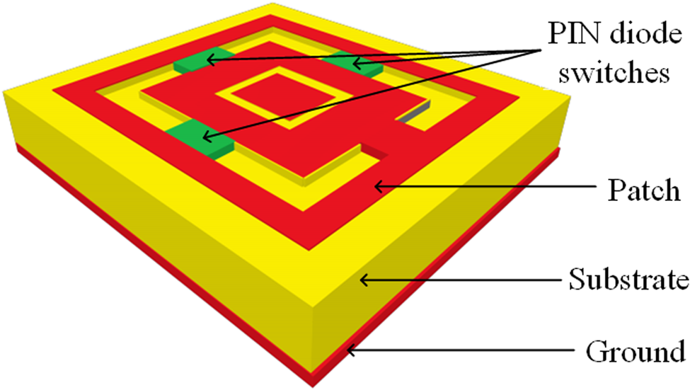
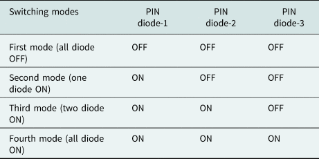
Figure 1 presents the three-dimensional view of the planned antenna structure. The substrate layer is designed using a low-profile material (FR-4). The dielectric constant is 4.4 for FR-4 material [Reference Patel, Lavadiya, Parmar, Ahmed, Taya and Das19]. Three PIN diodes were used for the charge distribution among different sections in the patch region, leading to reconfigurability. Table 1 shows the four switching modes. Due to the switching mechanism, the tunability of the frequency can be attained. In the first mode, all the PIN diodes are in the OFF condition. The second mode has one diode in the ON state and the rest of the two switching diodes in the OFF condition. The third mode has PIN diode-1 and PIN diode-2 in ON the condition, and PIN diode-3 in the OFF condition. Finally, the fourth model has all the PIN diodes in one condition.
Three-dimensional representation of the planned frequency reconfigurable patch antenna system. The bottom layer is made of FR-4 material. The breadth of the substrate material is 1.5 mm. The ground and patch layer are made of copper. The height of both these layers is 0.35 mm.

Switching states of the three PIN diodes for achieving frequency reconfigurability

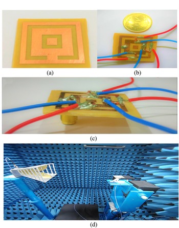
Figure 2 reveals the designed view of the proposed structure. Figure 2(a) presents the top view of the simple cropped patch without the PIN diodes. The top view of the patch with the three connected PIN diodes is shown in Fig. 2(b). The lateral view is observed in Fig. 2(c). Figure 2(d) shows an anechoic chamber. It is used for directivity measurement.
Designed model of the planned reconfigurable MPA. (a) The top view of the patch without attaching the PIN diodes. (b) The top view of the three PIN diode attached antenna structure. (c) The lateral view of the prototype with three PIN diodes. (d) Directivity finding using an anechoic chamber.

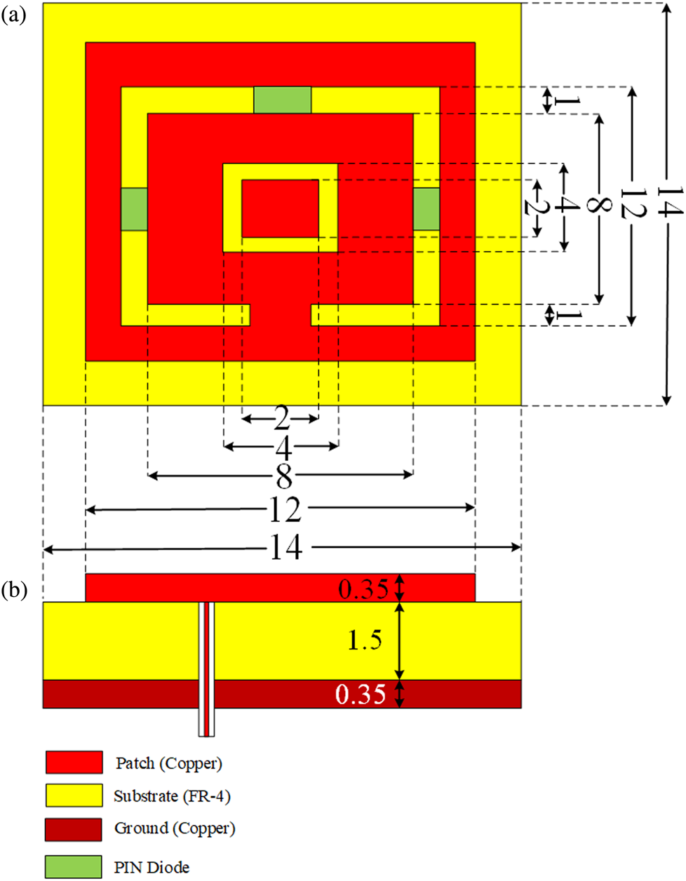
The top view of the MPA is shown in Fig. 3(a). Figure 3(b) shows the lateral view of the presented structure. The copper material is used in the patch of antenna and ground layer; both have a thickness of 0.35 mm. In this design, the size of the copper layer is 1 oz; 1 oz corresponds to 14 mils (0.3 mm). The size of the ground and substrate are 14 mm × 14 mm. The dimension of the patch is 12 mm × 12 mm. The patch area is cropped for attaching the PIN diode, which changes the energy distribution, resulting in frequency reconfigurability. Two gaps in the cropped area are 1 mm. The dimension of the inner area of the rectangle patch is 2 mm. After cropping, the inner area is 4 mm. After cropping the outer area, the dimensions are 8 mm.
(a) Design structure's top level schematic diagram. (b) The side view of the design. The coaxial feed mechanism is used for the energies of the patch. All dimensions are represented in mm.

The dimensions of the proposed antenna structure are calculated using equations (1)–(11) [Reference Sumathi, Lavadiya, Yin, Parmar and Patel20]. The resonance frequency of Split ring resonator (SRR) can be calculated using equation (1). Here, L represents the inductance and C represents the capacitance:

The effective relative permittivity of a metamaterial antenna is calculated as below:

The coefficients are calculated as per the following equations [Reference Patel, Shah and Kosta18,Reference Patel and Kosta28]:


The coefficients F 1, a 1, b 1, and relative electrostatic permittivity (ɛ es) are calculated as follows:


The S-parameters are required to analyze reflectance responses for the antenna structure in the gigahertz frequency range. The impedance and refractive index are required to calculate the transmittance (S 21) and reflectance (S 11) [Reference Patel, Kosta and Charola29]:


where n represents the refractive ratio, d represents the layer thickness, and z represents the wave impedance [Reference Lavadiya30].
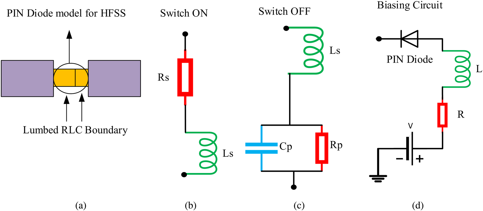
The switch OFF and ON mechanism of the presented architecture reflects frequency reconfigurability by switching the ON/OFF direction. The PIN diode is used as an RF switch. Figure 4 presents the equivalent electric circuit model of the PIN diode for the HFSS tool. Figure 4(a) presents two segments of a patch connected by the component R–L–C. The ON condition is presented in Fig. 4(b). In the ON configuration, resistor (Rs) and inductor (Ls) are connected in the series. The OFF condition is presented in Fig. 4(c); it is a series combination of resistor (Rp) and capacitor (Cp). The equivalent of both is connected with the inductor (Ls). The HPND 4005 model of PIN diode is used in the presented design. Planar beam lead PIN diode HPND-4005 has a high lead strength and excellent electrical performance. The PIN diode provides the resistance of 4.7 Ω and the smaller capacitance value of 0.017 pf. The biasing circuit is presented in Fig. 4(d). Furthermore, this PIN diode is very rugged. For simplicity, the antenna's reconfigurability was examined in terms of resistance, using the idea that the PIN diode functions as an open circuit for high resistor values and as a closed circuit for low resistor values [Reference Lavadiya30] (Table 2).
Equivalent model of PIN diode: (a) the lumped R–L–C model for the HFSS tool, (b) ON state model, (c) OFF state of the model, and (d) PIN diode biasing circuit.

Frequency tunability examination for different switching conditions

Simulation and fabricated design results
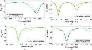
The graphical representation of reflectance response for the simulated and measured results for the switch ON and OFF configuration is presented in Fig. 5. There is some tolerance in both the results due to the limitation in the fabrication process. The large soldering area modified the path of charge propagation in the structure, affecting the design's characteristic impedance. The excessive path will also increase the effective length of the inductance. The capacitance is contingent on the gap between the two conducting regions. The gap between the two conducting regions decreases, affecting that region's capacitance [Reference Azarian, Lando and Pecht31]. Due to the variation in the capacitance and inductance, the resonance frequency is also affected – the resonance frequency change in the simulated and fabricated reflectance responses is shown in Fig. 5. The efficiency and thermal loss is affected due to the soldering. The thermal loss has been affected up to 0.3 dB. The effect in the high Q antenna for the high current has a more negligible effect on the thermal loss. The resistance loss of ~0.25 Ω is estimated [Reference Bahramzy, Jagielski and Pedersen32].
Reflectance coefficient plots for the three PIN diodes, switch-ON and OFF modes: (a) all switch OFF mode configuration, (b) one switch ON mode configuration, (c) two switches ON mode configurations, and (d) three switches ON configuration.

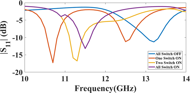
All switch OFF mode shows the reflectance response of −11.27 dB for the resonance of 13.2 GHz with the BW of 250 MHz as illustrated in Fig. 5(a). One switch ON mode signifies the first S 11 of −17.27 dB achieved at the resonating frequency of 10.7 GHz along with the BW of 250 MHz, and the second S 11 of −11.2 dB achieved at the resonating frequency of 12.5 GHz with the BW of 170 MHz, as illustrated in Fig. 5(b). Two switches ON mode represent the reflectance response of −16.75 dB achieved at the resonating frequency of 11.3 GHz with the BW of 340 GHz as illustrated in Fig. 5(c). All switch ON mode signifies the S 11 of −13.18 dB achieved at the resonating frequency of 11.5 GHz with the BW of 290 MHz as illustrated in Fig. 5(d). Table 3 presents the data in the tabular form for plot represented in (Fig. 6).
Reflectance plot for three switching conditions over the frequency range of 10–14 GHz. All switch OFF mode represents the reflectance of −11.27 dB at the 3.2 GHz frequency with a BW of 250 MHz. One switch ON mode shows the first reflectance of −17.27 dB at the 10.7 GHz frequency with a BW of 250 MHz and the second reflectance of −11.2 dB at the 12.5 GHz frequency with a BW of 170 MHz. Two switches ON mode represent the reflectance of −16.75 dB at 11.3 GHz frequency with a BW of 340 MHz. Finally, all switch ON mode shows the reflectance of −13.18 dB at 11.5 GHz frequency with a BW of 290 MHz.

Tabular illustration of switching modes, reflection response, frequency of resonance, BW, gain and the electric field for the performance analysis

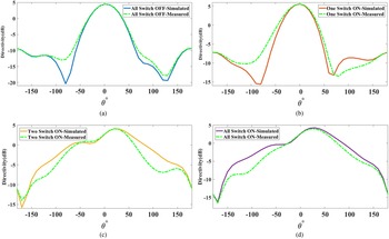
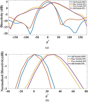
The one switch-ON mode yields the reflectance coefficient at 10.7 GHz, and all switch-ON mode provides the reflectance coefficient at 13.2 GHz. These represent that the maximum frequency tunability is 2.5 GHz. The radiation pattern behavior is analyzed based upon the directivity. Figure 7 illustrates the measured and simulated directivity plot of the switch OFF and ON modes over −180° to +180°. The directivity of mode-1 (all switch OFF mode), mode-2 (one switch ON mode), mode-3 (two switches ON mode), and mode-4 (all switch ON mode) is 4.46, 5.58, 4.08 and 4.22 dB, respectively. Good directivity is shown in all the mode configurations. Figure 8(a) shows the measured and simulated directivity plot. The normalized directivity for mode-1 (all switch OFF mode), mode-2 (one switch ON mode), mode-3 (two switches ON mode), and mode-4 (all switch ON mode) is respectively 56° (−26° to +30°), 55° (−30° to +25°), 85° (−15° to +70°), and 87° (−12° to +75°) as shown in Fig. 8(b).
Directivity plot for four modes. (a) All switch-OFF mode represents the highest directivity of 4.46 dB. (b) One switch ON mode represents the highest directivity of 5.58 dB. (c) Two switches ON modes represent the highest directivity of 4.08 dB. (d) All switch ON mode represents the highest directivity of 4.22 dB.

(a) Directivity plot for mode-1 (switch-off mode), mode-2 (one switch ON mode), mode-3 (two switches ON mode), and mode-4 (all switch ON mode) are respectively 4.46, 5.58, 4.08, and 4.22 dB over −180° to +180°. (b) The −3 dB down directivity for mode-1 (switch OFF mode), mode-2 (one switch ON mode), mode-3 (two switches ON mode), and mode-4 (all switch ON mode) are respectively 56°, 55°, 85°, and 87°.

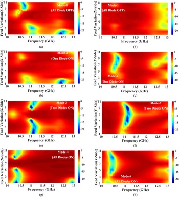
Figure 9 illustrates the Fermi (contour) plot of reflectance response for the different feed positions over the different PIN diode configurations. Figure 9(a) shows the feed variation in the X direction (1–11 mm) to identify the S 11 over the 10–13 GHz for mode-1. Three bands of S 11 are detected at 10.5, 11.1, and 12.5 GHz. Figure 9(b) shows the feed variation in the Y direction (1–11 mm) to observe the S 11 over 10–13 GHz for mode-1. There is one band of S 11 detected at 13 GHz. Figure 9(c) shows the feed variation in the X direction (1–11 mm) to observe the S 11 over 10–13 GHz for mode-2. Three bands of S 11 are detected at 10.8 and 12.5 GHz. Figure 9(d) shows the feed variation in the Y direction (1–11 mm) to observe the S 11 over 10–13 GHz for mode-2. Three bands of S 11 are detected at 10.53, 12.5, and 13 GHz for mode-2. Figure 9(e) shows the feed variation in the X direction (1–11 mm) to observe the S 11 over 10–13 GHz for mode-3. There is one band of S 11 observed at 11 GHz. Figure 9(f) shows the feed variation in the Y direction (1–11 mm) to observe the S 11 over 10–13 GHz for mode-3. There is one band of S 11 observed at 11.2 GHz. Figure 9(g) shows the feed variation in the X direction (1–11 mm) to observe the S 11 over 10–13 GHz for mode-4. There are three bands of S 11 detected at 10.25 and 13 GHz. Figure 9(h) shows the feed variation in the Y direction (1–11 mm) to observe the S 11 over 10–13 GHz for mode-4. There is one band of S 11 observed at 10.25 and 13 GHz. It is observed that reflectance responses also shift for the varying feed position [Reference Patel, Lavadiya, Kosta, Kosta, Nguyen and Dhasarathan9].
Reflectance coefficient analysis using Fermi plot for the different feed positions under the switch ON and OFF configurations. Variation of feed position in the X and Y directions is carried out for 1–11 mm over the 10–13 GHz frequency range.

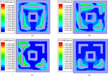
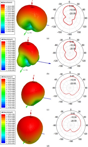
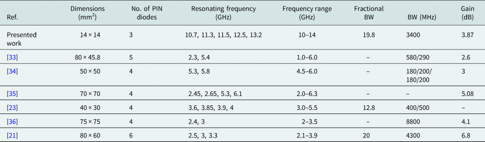
The electric field distribution for all modes is presented in Fig. 10. Electric fields for mode-1 (switch-OFF mode), mode-2 (one switch ON mode), mode-3 (two switches ON mode), and mode-4 (all switch ON mode) are respectively 16 993, 21 221, 46 558, and 15 051 v/m. The maximum electric field is observed in mode-3 (two switches ON mode). The efficiency of the structure can be observed based upon higher gain. The two-dimensional and three-dimensional gains for the different structures are illustrated in Fig. 11. Maximum gain for mode-1 (switch-OFF mode), mode-2 (one switch ON mode), mode-3 (two switches ON mode), and mode-4 (all switch ON mode) are respectively 3.38, 2.03, 3.87, and 0.9 dB. Table 4 compares the proposed work's performance to previously published work.
Electric field for mode-1 (switch-off mode), mode-2 (one switch ON mode), mode-3 (two switches ON mode), and mode-4 (all switch ON mode) are respectively 16 993, 21 221, 46 558, and 15 051 v/m.

Two-dimensional and three-dimensional gain patterns are presented. The maximum gain for mode-1 (switch-OFF mode), mode-2 (one switch ON mode), mode-3 (two switches ON mode), and mode-4 (all switch ON mode) are respectively 3.38, 2.03, 3.87, and 0.9 dB.

Performance observation of the presented work with earlier published work

Conclusion
The miniaturized and broadband frequency reconfigurable MPA design structure is presented in this study. The frequency tunability is attained using the three PIN diodes. The assessment of simulation and fabrication was carried out for reliability. The three PIN diodes are located on the patch area, and by switching them ON and OFF, four modes are analyzed and the results are presented. Many performance parameters are analyzed such as reflectance coefficient, BW, resonance frequency, electric field, feed position variation, and gain among different configurations. The unique features attained by the proposed design structure are the BW of 340 MHz, maximum frequency reconfigurability of 2.50 GHz, maximum directivity of 5.58 dB, normalized directivity of 87°, the electric field of 46 558 v/m, and the maximum gain of 3.87 dB. Performance observation of the presented work with previously published research work is also included. The presented design is used for radar, short-range tracking, missile guidance, and many more.
Conflict of interest
Authors declared no conflict of interest.
 Shobhit K. Patel received his Ph.D. in electronics and communication engineering from the Charotar University of Science and Technology, Changa, India. He is currently working in the area of photonics, metamaterial, antennas, optics, and artificial intelligence. He has published several research papers in high impact SCI journals. He has also filed seven Indian patents on different novel research. He received DST international travel grant in 2014 to present a paper in IEEE APS-URSI symposium at Memphis, USA. He also received DST international travel grant in 2017 to present a paper in PIERS symposium, NTU, Singapore. He has been named in the list of “Top 2% scientist worldwide identified by Stanford University” in 2021. He is currently working on many graphene-based projects and has received funding from SERB, DST, for his research. He has been honored with awards for the achievements in the area of the research field.
 Sunil P. Lavadiya received his M.Tech. degree in communication engineering from the Nirma University, Ahmedabad, in 2010. He is pursuing his Ph.D. in liquid antennas from Marwadi University. He currently works as an assistant professor in the Department of Information and Communication Engineering, Marwadi University. He has 12 years of teaching experience. His current research interests include liquid antennas, reconfigurable antennas, solar absorbers, and graphene-based polarizers. He has published 22 SCI papers, 15 Scopus papers, and 7 book chapters.
 Juveriya Parmar received her B.Sc. degree in physics from Saurastra University and her M.Sc. degree in physics from Marwadi University. She has recently joined as graduate research assistant at the University of Nebraska-Lincoln, Nebraska, USA. Before joining the University of Nebraska, Lincoln, she was employee of Marwadi University for 2 years, where she worked in the field of graphene, metamaterials, biosensors, and solar absorbers. She is currently working in the field of photonics, electromagnetics, materials, etc. She has published more than 27 SCI articles in international journals.
 Sudipta Das is currently working as an associate professor in the Department of Electronics and Communication Engineering at IMPS College of Engineering and Technology, West Bengal, India. He has 11 years of teaching experience and 8 years of research experience. He has contributed more than 100 research articles in various peer-reviewed international journals and conferences of repute. His research interests are microstrip antennas for microwave, mm-wave and THz communication systems, flexible antenna design, filter design, FSS, RFID, microwave components, and THz systems. Presently, he is working on the design and development of graphene-based THz antennas, modulation techniques for THz communication systems, metamaterials, graphene-based photonic structures, compact MIMO antennas, antenna arrays and filter design for 5G applications. He has authored one book on “Microstrip Filter Design,” edited two books on THz technology, and also contributed several book chapters. He is associated with different international journals as editorial board member. His biography is listed in Marquis Who's who in the World 2016. He has been conferred with the “Outstanding teacher in Electronics & Communication Engineering” award by Global Outreach Research and Education Summit Awards, in 2019.
 Kawsar Ahmed received his B.Sc. and M.Sc. engineering degrees in information and communication technology (ICT) from Mawlana Bhashani Science and Technology University, Tangail, Bangladesh. He has achieved gold medals for engineering faculty first both in B.Sc. (Engg.) and M.Sc. (Engg.) degrees from the university for his academic excellence. Currently, he is serving as an assistant professor in the same department and pursuing his Ph.D. degree on biomedical engineering at the University of Saskatchewan, Canada. Before that, he joined as a lecturer at the same department and software engineering department in Daffodil International University. He has published more than 250 publications in IEEE, IET, OSA, Elsevier, Springer, ISI, and PubMed indexed journals. He has published two books on bioinformatics and photonic sensor design. He is research coordinator of “Group of Biophotomatiχ.” He is also member of IEEE, SPIE, and OSA. He holds the top position at his department as well as university and is listed as the top 10 researchers in Bangladesh, 2020 to 2017, respectively (Scopus index based). His research group received SPIE traveling award and best paper award in IEEE WIECON ECE-2015 Conference. His research interests include biomedical engineering, biophotonics, biosensors, machine learning, federated learning, data mining, and bioinformatics.
 Sofyan A. Taya is a professor of theoretical physics – optoelectronics at Physics Department of Islamic University of Gaza, Palestine. He received his Ph.D. degree from Ain Shams University, Cairo, Egypt in 2007. He was selected among the top 2% of researchers around the world based on a study conducted by the global publishing house (Elsevier) and Stanford University in the USA (August 2021). He received Abdul Hameed Shoman Award for Young Arab Researchers, Jordan, 2012. He was awarded with young collaborator program award, international center for theoretical physics, ICTP, Italy, 2001. Professor Taya participated in many international and local conferences. He has published about 180 articles in international referred journals. He has supervised many graduate students. His research interests focus on the fields of integrated optics for sensor applications, waveguides, ellipsometry, OLEDs, numerical techniques, non-linear optics, applications of left-handed materials, and photonic crystals.