I. INTRODUCTION
Low-dimensional nanostructures, such as nanowires, nanorods, and nanobelts, have attracted a great deal of attention because of their unique characteristics and application in nanotechnology and material science.Reference Wang, Cai and Zhang1 The synthesis of single-crystal semiconductor nanowires with controlled size, morphology, and growth orientations is crucial as the functional properties of the nanowires are dictated by these structural parameters. The successful synthesis of silicon nanowires (SiNWs) has generated great interest in quasi-one-dimensional materialsReference Schmidt, Wittemann and Gösele2 because of their novel structural, surface, electronic, and mechanical properties. Nanowires, including nanorod-based solar cells, have attracted interest in recent years because of their characteristics and processing benefits.Reference Perraud, Poncet, Noël, Levis, Faucherand, Rouviére, Thony, Jaussaud and Delsol3 Combining silicon nanostructures with organic materials has been proposed to provide a large interface area between organic and inorganic components.Reference Huang, Hsiao, Syu, Chao and Lin4 Nanowire-enabled solar cells allow light absorption to be decoupled from the carrier transport direction, such that current densities can be improved in materials where the diffusion length of the minority carriers is much shorter than the thickness of the material required for optimal light absorption.Reference Huang, Hsiao, Syu, Chao and Lin4–Reference Dalchiele, Leinen, Marotti and Ramos-Barrado6
SiNW arrays can be fabricated by various techniques such as chemical vapor decomposition,Reference Lu, Li, Kong, Guo and Li7 dry etching, laser ablation,Reference Yu, Lee and Bello8 and the vapor–liquid–solid method.Reference Morales and Lieber9, Reference Yu, Chang and Heath10 A wet etching method has recently been developed to prepare aligned SiNW arrays with a high-quality monocrystalline phase, denominated here as self-assembly electroless metal deposition nanoelectrochemistry (referred to here as SAEMD-nanoelectrochemistry). It has attracted a great deal of attention owing to its low cost, low processing temperature, and simple fabrication procedure. The detailed fabrication process of SiNWs by this procedure has been reported in our previous workReference Dalchiele, Leinen, Marotti and Ramos-Barrado6, Reference Dalchiele, Martín, Leinen, Marotti and Ramos-Barrado11.
Arrays of vertically aligned SiNWs are expected to show mechanical properties that are different from bulk silicon and individual nanowires.Reference Teo, Huang, Zhang and Li12 Any practical application of these materials is likely to involve a large number of nanowires in close proximity to each other. Instrumented indentation has been the most commonly used method for studying the mechanical properties of films and coatings. In this work, the buckling instabilities of vertically aligned SiNW arrays have been studied by nanoindentation tests. The main parameters of an indented sample defined by the results from the nanoindentation technique are the hardness (H) and the Young’s modulus (E). It must be noted that the nanoindentation theory has been established for probing films and bulk materials with a semi-infinite half space.Reference Oliver and Pharr13 Hence, when this technique is used to characterize the mechanical properties of a wire-like structure, error in the resulting values could occur because the boundary conditions of the wire-like structure apparently differ from those of thin film and bulk materials.Reference Sohn, Park, Yoon, Song, Jee, Lee, Na, Kwon and Eom14–Reference Chang, Lin, Chen and Chang17 For this reason, the standard Oliver–Pharr method,Reference Oliver and Pharr13 valid for isotropic homogenous bodies, has not been used to analyze data in this work. On the basis of the Euler buckling model, the Young’s modulus and some other mechanical parameters have been estimated.Reference Young, Ji, Ghang, Fang, Hsueh, Meen and Chen18–Reference Riaz, Fulati, Yang, Nur, Willander and Klason21
When the tip radius of the indenter is much larger than the cross section of the SiNWs, there is no lateral resolution in the indentation system to identify the exact location of the indenter tip relative to a single SiNW. During an indentation test, a single nanowire first deforms and then becomes displaced. The critical load depends on the local contact friction between the indenter and the SiNWs. Also, it is necessary to take into account the inherently anisotropic nature of the specimens, the possible local inhomogeneities in the nanowire packing density, the dominant contribution of bending, and the cooperative buckling mechanism of the vertically aligned SiNWs to the indentation test response. This means that the mechanical behavior becomes very complex if one tries to simulate it in every detail. Therefore, to characterize the mechanical properties of the SiNW layer, it could be useful to extract some valid information from the force indentation curves.Reference Sohn, Park, Yoon, Song, Jee, Lee, Na, Kwon and Eom14–Reference Hsin, Mai, Gu, Gao, Huang, Liu, Chen and Wang16 After a first critical load is reached, if the maximum load is kept below the next critical load, the SiNW layer exhibits an elastic behavior for the next loading–unloading cycles.
II. EXPERIMENTAL
Monocrystalline SiNW arrays were formed by SAEMD-nanoelectrochemistry on p-type silicon wafer pieces in an ionic Ag/HF solution through selective etching. Single-side polished Si (100) wafer pieces with a thickness of 510–540 μm and a surface area of ∼1 cm2 were p-doped (B) (1.5–4.0 Ω cm resistivity) and washed in boiling acetone for 10 min and subsequently in isopropanol with sonication for 5 min at room temperature. They were oxidized in H2O2/HCl/H2O (2:1:8) at 353 K for 15 min to remove any traces of heavy metals and organic species, then rinsed copiously with deionized water, etched with 10% aqueous HF for 10 min, rinsed with water again, dried under a N2 stream, and immediately used as a substrate in the SiNW growth process. The cleaned Si wafer pieces were immersed in an aqueous HF/AgNO3 solution for 15–30 min at 50 °C (the concentration of HF and AgNO3 here were chosen to be 4.6 and 0.02 M, respectively). The length of SiNWs could be effectively controlled by adjusting the treatment time. The as-synthesized samples were then rinsed copiously in distilled water and dried at room temperature. Then, the SiNW arrays were dipped in 30 wt% HNO3 aqueous solution for 60 s. This was repeated several times to remove all residual Ag from the nanowire surfaces. After the nitric acid bath, no Ag peaks appeared in the x-ray photoelectron spectroscopy or x-ray diffraction (XRD) spectra of the SiNWs. The XRD pattern of the SiNWs (not shown here) indicates that the synthesized Si nanostructures are highly crystalline with various diffraction peaks corresponding to cubic silicon. (All products provided by Sigma-Aldrich, Madrid, Spain, except for silicon, provided by Topsil, Frederickssund, Denmark.)
The nanoindentation tests of surfaces formed by vertically aligned single crystal SiNWs were carried out using a MicroMaterials Nanotest equipment (MicroMaterials Limited). The MML NanoTest continuously controls and/or simultaneously measures the applied force, P, and the displacement, h, over a complete loading cycle. It also allows a limit to be set for a specified force P or displacement h, with ranges between 0 and 500 mN and between 0 and 50μm for P and h, respectively. The nanoindentation tests were carried out with a conical tip (60°), whose end can be considered spherical (10 μm radius). The radius of the tip was bigger than the transversal section of the individual SiNW. The thickness of the SiNW layer (32 ± 1 μm) was significantly larger than the depth of the indentation in all cases. The SiNWs were loaded to a prescribed force and then unloaded in a force-controlled mode. More than 100 different locations were tested to assess variability.
The characterization of the crystallographic properties of the as-formed SiNWs was done by transmission electron microscope (TEM) (PHILIPS CM-200) and XRD. XRD spectra were obtained with a Philips X′Pert PRO MPD using monochromatic radiation Cu Kα1 (λ = 1.5406 Å). Surface morphologies of the samples and the size distribution of the nanowires were characterized by a JEOL-JSN-5410 scanning electron microscope (SEM).
III. RESULTS AND DISCUSSION
A. Structural and morphological characterization
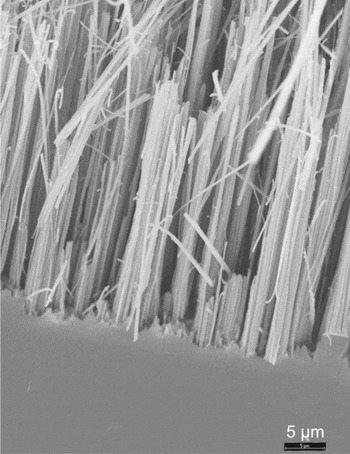
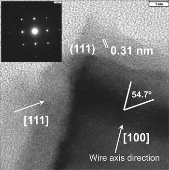
Figure 1 shows a SEM lateral side view of the SiNWs as obtained by SAEMD-nanoelectrochemistry on a p-type Si (100) substrate using 30 min etching. SEM observations reveal that large quantities of SiNW arrays could be produced on the silicon wafer piece. SEM images also show that the SiNWs are vertically aligned along and distributed across the entire substrate and that the density of the SiNW arrays for different times of etching undergeos little change. The approximate average dimensions of the nanowires analyzed by nanoindentation tests are estimated to be 341 ± 110 nm in diameter and 32 ± 1 μm in length, with an average density of 3.6 SiNWs/μm2. The morphology and structure of the SiNWs were characterized in detail using TEM and high-resolution transmission electron microscopy (HRTEM) analysis. HRTEM (Fig. 2) shows that SiNWs formed along the [100] direction. A further detailed analysis of HRTEM images by fast Fourier transform (FFT) (Fig. 2) indicates that the axial crystallographic orientation of the SiNWs is in the [100] direction, which is identical to the orientation of the initially used silicon wafers. In addition, the XRD peaks of the silicon (not shown here) indicate that the nanowires were vertically formed in the c-axis direction with good crystal quality.
Scanning electron microscope lateral image of the as-grown silicon nanowires (SiNWs).

High-resolution transmission electron microscopy of an individual SiNW and selected-area electron diffraction pattern.

B. Nanoindentation results
In general, when considering a single SiNW/nanorod under axial compression, two different deformation behaviors can be found, depending on the strength of the external loading. The first one can be viewed as an elastic deformation. The nanowire/nanorod retains its original atomic structures within a critical compressive force (critical load). The second behavior can be considered as a plastic deformation. Under the external loading beyond the elastic limit, the nanowire/nanorod no longer retains its original structure and undergoes dramatic structural deformation or buckling. The main indication of buckling is the presence of deformations in the direction of the compressive load that suddenly changes at a critical load into a transverse deformation, resulting in a sudden or catastrophic collapse of the nanowire/nanorod. In the case of the loss of the verticality, the nanowires are either broken or other inflection and critical points are produced. The critical buckling loads for a long column can be related to its end supports by the Euler model through the concept of an effective length (L e) by the following equationReference Nisbett and Budynas22:

where P c is the critical buckling load, E is the Young’s modulus, I is the second moment of area (I = π R 4/4 for the column, i.e., SiNW), and L e is the effective length. The effective length is expressed in terms of an effective-length factor K and the end-condition constant

where L is the actual length of the column. Thus, the critical load is given by

Therefore, the behavior of an ideal column compressed by an axial load P can be summarized as followsReference Nisbett and Budynas22:
(i) if P < P c, the column is in stable equilibrium in the straight position.
(ii) if P = P c, the column is in a neutral equilibrium in either the straight or a slightly bent position.
(iii) if P > P c, the column is in an unstable equilibrium in the straight position and will buckle under the slightest disturbance.
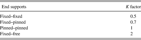
The buckling critical load decreases with an increase in the wire length, which is in agreement with the Euler theory. To obtain E from the former Eq. (3), we need to know K. To obtain K, we have supposed that a SiNW can be modeled as a vertical column with different end support conditions (see Table I).Reference Nisbett and Budynas22 Reported measurements of E for silicon nanobeams have demonstrated that the way in which the beam is clamped (i.e., the boundary conditions) affects the apparent value of E.Reference San Paulo, Bokor, Howe, He, Yang, Gao, Carraro and Maboudian23
K factor for different end supports.

For a Euler buckling column, the critical buckling strain ε c is given by

And the strain energy U is given by

where V is the volume of a single nanowire. The critical buckling stress σ c is related to the critical buckling load P c and the nanowire cross section A by

The slenderness ratio λ z is defined by

The Euler formula can only be used when the slenderness ratio of the nanowire is higher than that corresponding to a nanowire with a stress equal to the yield strength. The limit slenderness ratio can be defined as

where E is the Young’s modulus of the nanowire in a vertical direction and σ comp is the compression breaking strength as it is the same as the yield strength for ceramic materials. The Young’s modulus generally decreases as the mean diameter of the wire decreases.
This limit ratio gives the basis on which the columns are categorized:
(i) If the limit slenderness ratio is less than the actual slenderness ratio, then it is called long column and uses the Euler model.
(ii) If the limit slenderness ratio is greater than the actual slenderness ratio, then it is called intermediate column and uses the Johnson, Engesser, or Tetmajer models.
In our case, to find the ideal slenderness ratio, the values of Young’s modulus of bulk silicon with the same crystallographic orientation to that of our substrate (E [100] = 130 GPa and σ c = 0.49 GPa)Reference Lehmann24 were used, resulting in a limit slenderness of

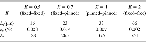
The effective length L e, the critical strain ε c, and the slenderness ratio λ z can be estimated for different end supports or K values considered for a single nanowire (see Table II). These parameters depend on the structure rather than on the material or on the load levels. For all K values, the effective slenderness ratio is higher than the limit slenderness ratio (λ lim < λ z). Therefore, the Euler model can be used. SiNW nanoindentation tests have shown that the behavior (load–displacement) of all the as-grown samples is approximately linear up to the first critical point.
Effective length L e, critical strain ε c, and slenderness ratio λ z corresponding to different end support conditions (K factors).

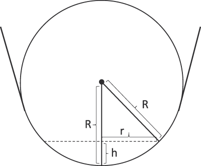
On the silicon substrate coated with the vertically aligned single crystal SiNWs that we are considering, the SiNWs are very close to each other. On the other hand, although the SiNWs grown are relatively homogenously distributed on the macroscopic scale, the SiNWs superficial density varies with location on the microscopic scale. The depth at the critical load (h) provides the projected area (A P) of the tip, and we have used A P to estimate the number of SiNWs that were axially loaded. As the end of the conical tip is spherical (Fig. 3), the projected area of the tip that is in close contact with the nanowires can be considered as the area of a circle of radius r.

Schematic representation of the end of the conical tip.

where D S is the superficial density of the nanowires obtained from SEM images.
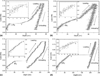
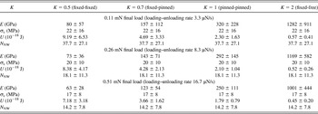
Because the tip radius of the indenter is much larger than the cross section of the SiNWs, there is not enough lateral resolution in the indentation system to identify the exact location of the indenter tip relative to a single SiNW. The smallest contact area for the average first critical load was around 0.30 μm2. Because the SiNW diameter has been estimated to be 341 ± 110 nm (0.09 μm2), the nanoindenter does not test the mechanical properties of individual SiNWs; nevertheless, the response is controlled by a small number of SiNWs, and it is susceptible to the local variations in the superficial densities of the SiNWs. Local SiNW density variations would be the main cause of the experimental deviations of the mechanical values obtained (Table III and Fig. 4). A direct contact on a rigidly pinned SiNW, or group of SiNWs, with the tip of the nanoindeter will cause a small indentation depth and area, and when the critical load is reached, the load-depth curve shows pop-in events [zone 0-1 in Figs. 5(a)–5(d)]. When the maximum load is increased (Fig. 6), new pop-in events appear at new higher critical loads. This suggests that after the first critical point, successive critical points would be reached, leading to the previously deformed SiNWs to display plasticity because of buckling events. If only the first critical load is considered, in which the straight prebuckling configuration of the SiNWs ceased, then the instability and buckling are a consequence of the verticality loss of the SiNWs under compressive overstresses. When the strain hardening for an individual nanowire/nanorod or bulk silicon is considered, this hardening is usually attributed to the increase in the dislocation density or kinking phenomenon,Reference Jain, Willander and Overstraeten25 which contributes to the plastic deformation of the individual silicon nanorod/nanowire.
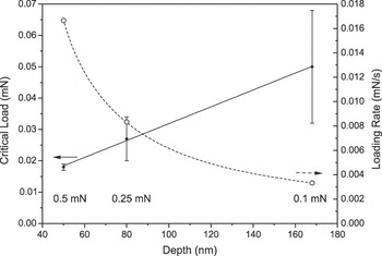
Critical loading and loading rate versus depth.

Four examples (a–d) of different behavior of load/unload versus displacement curves for a maximum load of 0.11 mN. The graphs inside correspond to the first lineal behavior (0 to 1).

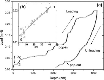
(a) An example of load/unload versus displacement curves for a maximum load of 0.26 mN. (b) First lineal behavior.

Young’s modulus (E), critical buckling strength (σ c), strain energy (U), and average number of nanowires under the tip at the maximum load N NW.

It must be pointed out that when referring to vertically aligned SiNWs, depending on the local superficial density of nanowires, impeded lateral displacement by lateral contact between nanowires could change the end support conditions (K). In continuum mechanics, buckling is a nonlinear structural phenomenon.Reference Nisbett and Budynas22 Figure 4 shows that the critical load decreases when the final load is increased and also the tip indents shallower into the layer. The increasing dispersion of the critical values obtained at lower final loads is related to the loading rate, such that the higher the loading rate, the lower the dispersion of critical loads. Figure 4 shows a nonlinear relationship between the critical load and the loading rate and a linear relationship with the depth reached. Therefore, the critical load depends mainly on geometrical factors, end supports, and the rate with which the load is applied.
In Fig. 6, the consecutive pop-in events and inflection points could be due to the displacement, deflection, or bending of the nanowires. A linear relationship exists up to the first critical point loading and deflection. Sometimes, the load–displacement curves at the higher maximum loads show pop-in events that could be due to a sudden release of the end of the SiNW from the tip of the indenter because of a release of the friction force. Also, the unload–displacement curve sometimes shows pop-out, which could be due to the release of elastic energy from the deformed SiNW layer.
In Fig. 6, the loading–displacement graph shows multiple zones. In zone 0-1, the load–displacement is linear. For this zone, the data show displacement to be proportional to the increase in load. This displacement corresponds to a situation in which the SiNWs are almost vertical and stable. The linear behavior is followed by a sharp change in the load–displacement curve at essentially the same force and the curve becomes flat (i.e., zone 1-2). Point 1 corresponds to a critical equilibrium configuration of the nanowires. The force applied at this point is the first critical load. Using the SiNWs superficial density as obtained from SEM images and considering the nanoindenter tip projected area (the Diamond Area Function), the average critical load for an individual nanowire can be determined. After the first inflection point of the loading portion, an increase in load results in the nanowires adopting a buckled configuration (Fig. 6). After the first critical point 1, the nanowires usually either break at the top, leading to the tip going deeper into the SiNW layer, or develop multiple buckling points, leading to fracture. The alternative buckled configurations become strain hardened and greater force is required for buckling to occur again.
The effective modulus of elasticity, critical strength, and strain energy for a single SiNW have been estimated for the four configurations shown in Table II. The three parameters (L e, ε c, λ z) depend on the configuration and geometrical relationships. This is because buckling failure is a design or structure failure rather than a material failure. The estimated values are given in Table III, together with the number of the SiNWs involved in the first critical load for three different maximum loads. We have used the same strain rate (strain rate = current load/loading rate) for the three maximum load levels, giving three different rates of loading/unloading.
The load at the first critical point of the load–displacement curve is divided by the number of SiNWs that were estimated to be axially loaded. The single SiNW critical strength is obtained as the average critical load.
As shown in Table III, when the maximum load is increased (higher rates of loading–unloading), the Young’s modulus obtained decreases. This could be due to the effect of the applied load rate on the first critical load. The load rate could also have an effect on the response of the previously deformed SiNWs.
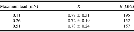
The results in Table III indicate that higher maximum loads (higher loading rates) imply a lower Young’s modulus and critical stress. This tendency can be explained by assuming that higher loading rates overload SiNWs in higher dislocation densities, and therefore, the SiNW becomes more brittle. Depending on the boundary conditions chosen, the Young’s modulus values found here are close to those of the bulk silicon values. Ma et al.Reference Ma, Wang, Zhao and Wang26 and Lee et al.Reference Lee and Rudd27 have investigated the mechanical properties of SiNWs with various diameters and growth directions using first-principle methods. They found that the Young’s modulus of nanowires increases slowly with wire size and would approach the bulk value at a certain critical cross section size (2–5 nm corresponding to 90–130 GPa). Because this critical size is lower than the cross section of our SiNW, it is to be expected that the Young’s modulus would be close to that of the bulk value. In the horizontal bending test, it was found that SiNWs with diameters >100 nm have a Young’s modulus close to that of the bulk value. Shon et al.Reference Sohn, Park, Yoon, Song, Jee, Lee, Na, Kwon and Eom14 and Kang et al.Reference Kang, Li, Ho and Huang28 have found a Young’s modulus in the range of 140–160 GPa for nanowires in the range of 100–600 nm. San Paulo et al.Reference San Paulo, Bokor, Howe, He, Yang, Gao, Carraro and Maboudian23 have found similar results for single-pinned nanowires of 120–190 nm (186 GPa). Vertical buckling tests, similar to ours but carried out in an AFM device, have given a Young’s modulus of 175 GPa for double-pinned nanowires with diameters in the range of 40–90 nm.Reference Hsin, Mai, Gu, Gao, Huang, Liu, Chen and Wang16 Molecular dynamic simulations for nanowires of 4 nm in diameter and a double-pinned boundary conditionReference Jing, Meng and Gao29 have shown a Young’s modulus of 110.4 GPa. Collins et al.Reference Collins, Giardini, Leistner and Kenny30 measured the Young’s modulus of silicon for different crystal orientations and obtained 130, 169, and 187 GPa for the [100], [110], and [111] directions, respectively. If it is supposed that the actual effective Young’s modulus is E = 130 GPa for the individual SiNW in the axial direction [100], then an effective K factor can be estimated through the Euler critical load formula by using the value of the average first critical load obtained from the experimental load–displacement curves for different final loads (Table IV). This effective K value should fit the theoretical boundary conditions with the real ones.
Effective K factors for different final loads and estimates of Young’s modulus corresponding to the K medium value.

The effective K values (Table IV) are quite similar for the three final loads, and therefore, it can be considered that the displacements of the SiNWs are subject to the same restrictions. The results of effective K values suggest a boundary condition where one end is fixed and the other end is pinned (fixed–pinned), with some contribution of both ends pinned (pinned–pinned), and both ends fixed (fixed–fixed). This could be justified by the fact that more than one SiNW is tested at each nanoidentation load/unload cycle and, depending on the friction between the end of the SiNWs and the curved surface of the tip of the indenter, the behavior of an individual SiNW could depend on the different end conditions. It could also be a consequence of a loaded group of SiNWs whose lateral movement is partially impeded. Finally, the Young’s modulus estimated by the interpolated values of the calculated average values of the Young’s modulus from experimental critical loads (Table III) at the effective K (Table IV) is in the range of the bulk silicon Young’s modulus.
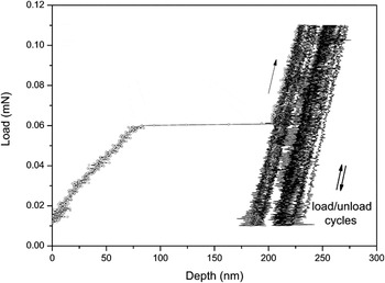
After the first load–unload cycle, if load/unload cycles are applied at the same point and the maximum load is not increased and the other indentation parameters are kept constant, the SiNWs behave in a similar way to an elastic solid while behaving with a greater stiffness and hardness in a converse situation. Figure 7 shows the elastic behavior when a sample is loaded at the same point by cyclical load/unload after having reached the critical load. We can also find similar behavior with more residual plastic deformation between individual cycles of load/unload. The mechanical response at the same point of the SiNWs when the maximum load is increased is going to be more resistant to plastic deformation. Further hardening could be due to a compacted SiNW layer with a plastic–elastic behavior. Finally, the deformed SiNW layer behaves like a porous film.
Cyclical load/unload applied at the same point for a maximum load of 0.11 mN.

IV. CONCLUSIONS
The main focus in this study was the experimental observation and characterization of the bending flexibility and buckling failure phenomena of vertically aligned single crystal SiNWs at the initial load/unload cycles. The SiNWs behavior is due to the contribution of the bulk silicon mechanical properties, the geometrical dimensions of the SiNWs, and the impeded lateral displacement. This last factor is due to the superficial density of the SiNWs. The estimated Young’s modulus is dependant on the loading rate applied. We have used the Euler model for long columns for the evaluation of the effective modulus of elasticity, critical strength, critical strain, and strain energy by supposing different K (end supports). Also, by using the reported bulk Silicon mechanical properties, we have estimated the effective K factors that correspond to the actual end conditions of the SiNWs. We also conclude that SiNWs show flexibility and plasticity after the first critical point. At higher loads, the mechanical behavior does not appear to be due to the buckling of individual nanowires, and therefore, the deformed SiNW layer could be considered as a plastic–elastic porous layer.
ACKOWLEDGMENTS
The authors are grateful to MICINN of Spain, for the financial support received (TEC2007-60996 and Consolider Ingenio 2010 CSD2008-00023). E.A.D. and R.E.M. also acknowledge the financial support of PEDECIBA-Física, and especially C.S.I.C., Consejo Superior de Investigaciones Científicas, Universidad de la República, Montevideo, Uruguay.