Metatronic circuitry has emerged as a promising technology platform for the development of high-throughput integrated optical circuitry for processing photons using parameterized and modular circuit elements, namely resistors (R), capacitors (C), and inductors (L), in analogy with conventional radio-frequency (RF) microelectronic circuitry,[ Reference Engheta, Salandrino and Alù 1 – Reference Engheta 5 ] but with the promise of operating at much smaller and faster scales in the infrared (IR) and visible regimes. Different from their RF counterparts, the non-negligible electric field inside dielectric/metallic (plasmonic) nanoparticles is responsible for the flow of an optical displacement current density,[ Reference Engheta 5 ] which plays a significant role, more relevant than the conduction current density, which dominates at lower frequencies, i.e., RF and microwaves. The optical input impedance of an arbitrary nanoparticle can be defined, consistently to the conventional impedance of an RF circuit element, as the ratio between the average potential difference at its terminals and the optical displacement current across it.[ Reference Alù and Engheta 6 ] Following this definition, the concept of metamaterial-inspired optical nanocircuitry was first introduced in[ Reference Engheta, Salandrino and Alù 1 , Reference Engheta 2 ] based on nanoparticles with plasmonic [negative real part of permittivity, Re(ε) < 0] and dielectric [positive real part of permittivity, Re(ε) > 0] materials, respectively acting as nanoinductors and nanocapacitors for optical fields. The non-zero imaginary part of permittivity [Im(ε)≠0] can synthesize a localized nanoresistor. The combination of optical lumped elements may offer wide possibilities to build nanocircuits for numerous optical applications. Recently, passive metatronic circuitries have been experimentally demonstrated, with applications ranging from stereo bandpass and bandstop nanofilters,[ Reference Sun, Edwards, Alù and Engheta 3 , Reference Caglayan, Hong, Edwards, Kagan and Engheta 4 ] to tuning and matching nanoantennas,[ Reference Alù and Engheta 7 – Reference Liu, Wen, Zhao, Wang, Nordlander, Halas and Alù 9 ] to higher-order circuitry made of complex clusters of resonant nanoparticles.[ Reference Fan, Wu, Bao, Bao, Bardhan, Halas, Manoharan, Nordlander, Shvets and Capasso 10 , Reference Shi, Elias, Monticone, Wu, Ratchford, Li and Alù 11 ] However, to bring these nanocircuits to the functional level of RF microelectronic circuits, active and nonlinear elements must be explored. The overarching goal of this work is to enrich the concept of metatronics by introducing nonlinear mixing and modulation at IR wavelengths using modular nanocircuit elements.
Modern communication schemes typically require nonlinear and active components for amplitude and frequency modulation, demodulation, and multiplexing.[ Reference Goldsmith 12 ] For instance, frequency mixers are nonlinear circuit elements commonly used to upconvert and/or downcovert the input signal into orthogonal high-/sub-harmonic output signals.[ Reference Goldsmith 12 ] As another example, all-optical switching relies on nonlinear self-amplitude modulation, as a self-action of intense pulsed light. Recently, nonlinear metatronic elements have been proposed using subwavelength plasmonic junctions, e.g., a metallic dipole nanoantenna loaded with nonlinear optical materials.[ Reference Chen, Farhat and Alù 13 – Reference Harutyunyan, Volpe, Quidant and Novotny 23 ] Surface plasmon resonances, as a coherent excitation of conduction-band free electrons, may substantially enhance the local field intensity in the vicinity (particularly in the gap region) of plasmonic nanostructures, thereby boosting otherwise weak optical nonlinearities. Several nonlinear elements for IR and optical circuitry have been proposed to realize specific nonlinear functions, such as phase conjugation,[ Reference Chen and Alù 14 ] difference frequency generation,[ Reference Chettiar and Engheta 18 ] frequency multiplication, all-optical bistable switching,[ Reference Chen, Farhat and Alù 13 , Reference Noskov, Belov and Kivshar 20 ], and spatial multiplexing,[ Reference Maksymov, Miroshnichenko and Kivshar 21 ] as well as diode[ Reference Mahmoud, Davoyan and Engheta 24 ] and transistor[ Reference Chettiar and Engheta 25 ] functionalities within the metatronics paradigm. However, these nonlinear elements necessitate proper loading of nonlinear nanoparticles (e.g., epitaxial III–V compounds), accurate fabrication of complicated geometry (e.g., isolated nanostructure arrays), and integration. In the following, we propose and theoretically investigate an effective layout for nonlinear metatronics, achieving subwavelength IR elements with large nonlinear response in a simple planarized geometry.
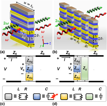
The geometry of interest, shown in Fig. 1(a), is formed by dissimilar plasmonic junctions of periodic silver (Ag)-tantalum pentoxide (Ta2O5)-gold (Au) films. We also study a higher-order nanocircuit, shown in Fig. 1(b), where the transverse gaps as shunt nanocapacitors may provide more flexibility in tuning frequency responses. The corresponding nanocircuit models for these metatronic devices are shown in Figs. 1(c) and 1(d). Using an atomic scale Ta2O5 insulating layer, which can be precisely controlled by atomic-layer deposition, the quantum conductance due to multiphoton-assisted electron tunneling through a metal–oxide–metal (MOM) nanojunction may be controlled.[ Reference Zuloaga, Prodan and Nordlander 26 – Reference Grover and Moddel 33 ] This quantum conductance has nonlinear components, effectively introducing a nonlinear nanoresistor in parallel to the nanocapacitor formed by the MOM structure. Indeed, it has been recently observed experimentally and studied theoretically that the power dissipation due to quantum conductance may set an upper limit to the quality factor and maximum possible field enhancement in plasmonic nanostructures.[ Reference Zuloaga, Prodan and Nordlander 26 , Reference Haus, de Ceglia, Vincenti and Scalora 29 – Reference Chen and Farhat 32 ] When an intense pulsed laser illuminates the IR nanocircuit of Fig. 1, within the quantum mechanical regime, the photon-assisted tunneling (PAT) process can induce relevant second-order and other higher-order nonlinearities in dissimilar MOM junctions, enabling a variety of nonlinear optical functions, such as rectification,[ Reference Grover and Moddel 33 ] second-/third-harmonic generation,[ Reference Haus, de Ceglia, Vincenti and Scalora 30 ] and two-photon absorption (TPA).[ Reference Haus, de Ceglia, Vincenti and Scalora 29 – Reference Chen and Farhat 32 ]
Schematic diagrams of: (a) a metatronic circuit made of periodic dissimilar plasmonic nanojunctions, (b) a higher-order circuit obtained adding shunt air-gap capacitances. Panels (c) and (d) are the corresponding nanocircuit models. The electric field is perpendicular to the semi-infinite nanorods (x-axis), forming a series combination of lumped circuit elements. After considering the quantum effect of multiphoton-assisted tunneling, flatland nanocircuits made of dissimilar MOM superlattices can exhibit efficient nonlinear optical effects.

Assuming an e
−iωt
time-harmonic dependence for the structure in Fig. 1(a), when the IR electric field is perpendicular to the x-axis, the proposed geometry operates as a series combination of lumped impedances Z
Ag = (ih)/(2εAgε0
ω
wL), Z
Au = (ih)/(2εAuε0
ω
wL), and
 ${Z_{\rm ox}} = (ig_1)/({\varepsilon_{{{\rm T}_2}{{\rm O}_5}}}{\varepsilon _0}\omega {wL})$
, which result in an equivalent surface impedance Z
eq = Z
Au + Z
Ag + Z
ox, where ε
0 is the free-space permittivity, w and L are the width and length of the semi-infinite metal and oxide nanostrips, h and g
1 are the thickness of metal nanostrips and oxide films [see Fig. 1(a)]. The relative permittivities of Au and Ag, ε
Au(ω) and ε
Ag(ω), are assumed to follow a Drude-type dispersion,[
Reference Johnson and Christy
34
,
Reference West, Ishii, Naik, Emani, Shalaev and Boltasseva
35
] (Below the onset of metal's interband transition, the relative permittivity of metal following the Drude-type dispersion model:
 ${\varepsilon _m} = {\varepsilon _\infty} - \omega _p^2 /[\omega (\omega + i\gamma )]$
, where the empirical parameters for Au are ω
p/2π = 2449 THz, γ/2π = 16.68 THz and ε
∞ = 6.9, and those for Ag are ω
p/2π = 2221 THz, γ/2π = 4.83 THz and ε
∞ = 3.7) and in the IR region the relative permittivity of Ta2O5,
 ${\varepsilon_{{\rm Ta}_2}}{\rm O}_5 = 4.4$
.[
36
] From the lumped element circuit model in Fig. 1(a), the transmittance of incident optical signals can be calculated as T = tt
* with the complex transmission coefficient t = Z
eq/(Z
eq + Z
0/2), where Z
0 = η
0(g
1 + h)/w and η
0 = 377 Ω (wave impedance of free-space). The transmittance of the higher-order circuit in Fig. 1(b) can be similarly obtained by modifying the characteristic impedances to Z
0 = η
0(g
1 + h)/(g
1 + w) and Z
eq = [(Z
Au + Z
Ag + Z
ox)−1 + Z
g
−1]−1, where the capacitive air-gap impedance Z
g = i(g
1 + h)/(ε
0
ωg
2
L).
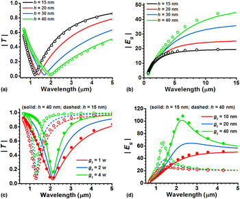
Figures 2(a) and 2(b) compare the transmission coefficients and the electric field enhancement factor inside the MOM nanojunction (neglecting quantum nonlocal effects[ 37 ]) for the structure in Fig. 1(a), with geometric parameters L = 10 nm, g 1 = 0.8 nm, and h (15, 20, 30, 40 nm). Results calculated using the metatronic circuit theory and full-wave simulations are shown with lines and dots, respectively. It is clear that IR band-notch filters can be quantitatively designed using the circuit approach, in analogy with.[ Reference Sun, Edwards, Alù and Engheta 3 ] Since the electric field is approximately uniform in the oxide region,[ Reference Sun, Edwards, Alù and Engheta 3 , Reference Caglayan, Hong, Edwards, Kagan and Engheta 4 ] the electric field enhancement factor inside the MOM nanojunctions can be calculated using the circuit model in Fig. 1(c) as the voltage drop across the oxide impedance divided by the oxide thickness (e.g., E g = V g /g 1). The analytical circuit model well describes the structure, provided that the dimensions of metallic and oxide nanostrips are subwavelength. Figs. 2(c) and 2(d) refer to the nanocircuit in Fig. 1(b) with different widths of the air gap, which affects the shunt impedance Z g (solid and dashed lines correspond to h = 15 nm and h = 40 nm). Here a non-negligible parasitic capacitance Z par = 0.2 Z ox in parallel to Z ox (due to the effect of fringing fields in the air region), with its value extracted from full-wave simulations, was introduced to improve the accuracy of our analytical model. By introducing the capacitive element, Z g, the quality factor, bandwidth, and local field enhancement at resonance can be tailored by varying the g 2/w ratio. Also a larger local field enhancement and Q-factor, which are particularly beneficial for the tunneling-induced nonlinear optical effects, may be obtained with a higher-order nanocircuit. In both types of nanocircuits, the resonance frequency is red-shifted when the metal thickness increases, which also increases the local field strength across the MOM tunnel junction.
(a) Transmission coefficient and (b) electric field enhancement (inside the MOM heterojunction) against wavelength for the metatronic circuit in Fig. 1(a) in the classical regime (lines, circuit theory calculations; dots, full-wave simulation results). Panels (c) and (d) are similar to (a) and (b), but for the metatronic circuit in Fig. 1(b).

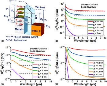
In the quantum regime, the proposed nanocircuits can support non-trivial nonlinear optical responses within the MOM tunneling barrier shown in Fig. 3(a). In the general scenario, the voltage applied to the MOM structure is a combination of optical (ac) and dc signals V(t) = V dc + (1/2)(V ω e −iωt + c.c). From the Tien–Gordon theory of multiphoton-assisted tunneling,[ Reference Tien and Gordon 38 , Reference Truker 39 ] the time-dependent wavefunction for electrons in metal becomes
 $$\eqalign{\psi (\bar{\bf r}, t) & = {\psi _0}(\bar{\bf r}, t)\exp \left[ { - i/\hbar \int_{}^t {qV(t^{\prime}){\kern 1pt} dt^{\prime}}} \right] \cr & \quad = {\psi _0}(\bar{\bf r}, t)\sum\limits_{n = - \infty} ^{n = + \infty} {{J_n}\left( {{{qV_\omega} / {\hbar \omega}}} \right){e^{ - in\omega t}},}} $$
where q is the electron charge,
 $\hbar $
is the reduced Planck constant,
 ${\psi _0}(\bar{\bf r}, t)$
is the unperturbed Schrödinger wavefunction, and J
n
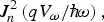
(·) is the nth order Bessel function. The modified wavefunction implies that optical signals adiabatically modulate the electron potential energy. The monochromatic electromagnetic field may therefore excite quantum-well virtual states separated from the unperturbed ground state by
 $ \pm n\hbar\!\omega $
, where n corresponds to the number of photons absorbed or emitted, with probability
 $J_n^2 \left( {{{qV_\omega} / {\hbar\!\omega}}} \right),$
by an electron at the metal surface. As a result, the time-dependent current is in the form of a Fourier series
 $I(t) = \sum\limits_{m = 0}^{m = + \infty} {1/2\left( {{I_{m \omega}} {e^{ - im\omega t}} + c. c.} \right)} $
,[
Reference Tien and Gordon
38
,
Reference Truker
39
] where the strengths of current components are given by
 $${I_{\rm illum}} = \sum\limits_{n = - \infty} ^\infty {J_0^2 \left( \alpha \right)} {I_{\rm dark}}\left( {qV_{dc}+ n\hbar\!\omega} \right),$$
 $$I_{m\omega} = \sum\limits_{n = - \infty} ^\infty {J_n}(\alpha ) \left[ J_{n + m}(\alpha ) + J_{n - m}(\alpha ) \right]I_{\rm dark}(qV_{dc} + {n\hbar}\!\omega ),$$
where
 $\alpha = q{V_\omega} /\hbar\!\omega $
, I
illum and I
mω
represent the dc (m = 0) and mth frequency-dependent currents under illumination. At IR and visible wavelengths, where α is typically small, and below the photoionization threshold, the summations in (2) can be expanded to higher orders in the voltage[
Reference Grover and Moddel
33
,
Reference Tien and Gordon
38
,
Reference Truker
39
]:
 $${I_{\rm illum}} = {I_{\rm dark}}({V_{\rm dc}}) + G_0^{(2)} {\left \vert {{V_\omega}} \right \vert ^2} + O{(\alpha )^4},$$
 $${I_\omega} = G_\omega ^{(1)} {V_\omega} + G_\omega ^{(3)} {\left \vert {{V_\omega}} \right \vert ^2}{V_\omega} + O{(\alpha )^5},$$
 $${I_{2\omega}} = G_{2\omega} ^{(2)} V_\omega ^2 + O{(\alpha )^4},$$
where
 $G_\omega ^{(1)} $
is the quantum conductance in the linear region, and G
(0), G
(2), G
(3), … are nonlinear quantum conductances that arise in an intense optical field. Typically, the contribution of nonlinearities higher than the third-order term can be ignored. The expressions for the linear and nonlinear quantum conductance are derived in the Supplementary Material. The tunneling dark current I
dark flowing between two dissimilar metal electrodes can be calculated using the well-known Simmons’ quasi-analytical formula[
Reference Simmons
40
–
Reference Simmons
42
] (see the Supplementary Material for details). Here
 $G_{2\omega} ^{(2)} \;and\;G_\omega ^{(3)} $
are quantum conductances associated with second-harmonic generation (SHG) and TPA nonlinear optical processes, respectively. Here we ignore the third and other high-order harmonics, i.e., m > 3, and, in the absence of a dc load line, there is no dc power consumption due to the dark current I
dark(V
dc) and the rectified dc current
 ${I_{\rm rect}} \approx G_0^{(2)} {\left\vert {{V_\omega}} \right\vert^2}.$
Figures 3(b)–3(d) respectively show the spectrum of normalized first-order (linear), second-order, and third-order quantum conductances
 $G_\omega ^{(1)} \times {g_1}/(wL)$
,
 $G_{2\omega} ^{(2)} \times g_1^2 /(wL)$
, and
 $G_\omega ^{(3)} \times g_1^3 /(wL)$
for an Ag–Ta2O5–Au junction with different thicknesses of Ta2O5 nanofilm. We used the realistic work functions for Ag and Au: ΦAg = 4.26 eV and ΦAu = 5.1 eV, and the static relative permittivity and electron affinity of Ta2O5 are K = 20 and χ = 3.86 eV.[
Reference Grover and Moddel
43
] It is seen that linear and nonlinear components of quantum conductance can be greatly enhanced by reducing the Ta2O5 thickness, which narrows the potential barrier for electron tunneling and therefore increases the dark current. At high photon energies (or short IR wavelengths), the values of
 $G_\omega ^{(1)} $
and
 $G_{2\omega} ^{(2)} $
are much higher than what expected from purely classic considerations (dashed lines). Moreover, the highly localized electric fields due to the plasmon coupling may enhance any nonlinearity induced inside the nanogap, thus enabling the observation of nonlinear optical effects with reasonable light intensity.
(a) Schematic diagrams of multi-PATin a dissimilar MOM junction. Normalized (b) first-order (linear optical), (c) second-order, and (d) third-order quantum conductance for an Ag–Ta2O5–Au junction in Fig. 1(a), with different separations between two metals. Dashed lines in (b) and (d) represent the classical limits
 $G_{\omega, {\rm classic}}^{(1)} {g_1}/(hL) = (\partial {I_{\rm dark}}/\partial {V_{\rm dc}})\left\vert {_{{V_{\rm dc}} = 0}} \right.$
and
 $G_{2\omega, {\rm classic}}^{(2)} g_1^2 /(hL) = (1/4)({\partial ^2}{I_{\rm dark}}/\partial V_{\rm dc}^2 )\left\vert {_{{V_{\rm dc}} = 0}} \right.$
.

Considering the quantum mechanical PAT effect in MOM nanojunctions, it is also necessary to introduce a shunt tunneling-induced nanoresistor
 $R_Q^{(1)} = {\left( {G_\omega ^{(1)}} \right)^{ - 1}}$
into the lumped circuit model of Figs. 1(b) and 1(c). In addition, a nonlinear nanoresistor
 $R_Q^{(3)} = {\left( {G_\omega ^{(3)} {{\left\vert {V_g^{}} \right\vert}^2}} \right)^{ - 1}}$
, responsible for the TPA at intense illumination, could detune the electric field E
g
(or voltage V
g
) inside the nanogap. Since electric fields are reasonably uniform inside the T2O5 layer, according to the circuit model in Fig. 1, the electric field across the T2O5 nanofilm is given by V
g
= (Z
ox
V
ω
)/(Z
Au + Z
Ag + Z
ox), where the quantum-corrected oxide impedance now becomes
 $Z_{\rm ox} = i/(\omega C_{\rm ox}) + R_Q^{(1)} + R_Q^{(3)}$
, where C
ox is the electrostatic capacitance. We note that a transcendental equation must be iteratively solved to evaluate the exact value of local electric field.[
Reference Chen, Farhat and Alù
13
] In addition, the induced nonlinear currents (e.g., I
2ω
, I
3ω
, …) will produce higher-harmonics (e.g., SHG, THG, …) on both sides of the subwavelength structure in Fig. 1.[
Reference Chen and Alù
14
] Fortunately, higher harmonic signals other than the desired one can be filtered out through the design of IR lumped element circuit. For the nanocircuit in Fig. 1(a), the SHG output power can be analyzed using the reduced Norton equivalent circuit in the inset of Fig. 4(a) and is given by:
 $$P_{2\omega} ^{(2)} = \displaystyle{{{Z_0}} \over 4}{\left \vert {\displaystyle{{{I_{2\omega}} {Z_{\rm ox}}\left( {2\omega} \right)} \over {{Z_{\rm Cu}}\left( {2\omega} \right) + {Z_{\rm Al}}\left( {2\omega} \right) + {Z_{\rm ox}}\left( {2\omega} \right) + {Z_0}/2}}} \right \vert ^2},$$
where the nonlinear current
 ${I_{2\omega}} = G_{2\omega} ^{(2)} V_g^2 $
is determined by the local electric field E
g
= V
g
/g
1 The SHG conversion efficiency for the device in Fig. 1(b) can be similarly calculated using the Norton equivalent circuit. Considering harmonic balance and power conversation, the incident power P
inc must equal the sum of power dissipation at the fundamental and second harmonics:
 ${P_{\rm inc}} = {\left\vert {{V_0}} \right\vert^2}/\left( {2{Z_0}} \right) \approx \left( {{1 / 2}} \right){V_\omega} I_\omega ^{\ast} + \left( {{1 / 2}} \right){V_{2\omega}} I_{2\omega} ^{\ast} $
, where V
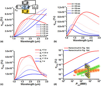
0 is the applied voltage, V and I are the voltage and current flowing through the surface impedance of the periodic MOM-superlattice structure. Figs. 4(a) and 4(b) show the spectral SHG conversion efficiency
 ${\eta _{\rm shg}} = P_{2\omega} ^{(2)} /{P_{\rm inc}}$
at the second-harmonic frequency for the structure in Fig. 1(a), varying the metal thickness; here the pump intensity is 40 MW/cm2. Figs. 4(a) and 4(b) reveal that in the long-wavelength region the SHG efficiency increases with frequency, since in the quantum regime
 $G_{2\omega} ^{(2)} $
, as seen in Fig. 3(c), becomes larger at higher photon energy. However, the SHG efficiency saturates in the vicinity of the cut-off wavelength of the circuit. We should note that the nanocircuit may be further optimized to accomplish a dual resonance at the fundamental and second harmonics (e.g., by introducing more lumped elements), which may accordingly increase the SHG conversion efficiency.
SHG conversion efficiency for (a) the metatronic circuit in Fig. 1(a) with different metal thicknesses (varying Z Au and Z Ag), and the metatronic circuit in Fig. 1(b), with (b) different thicknesses of metal (varying Z Au and Z Ag) and (c) different widths of air gap (varying Z g). The inset of (a) shows the reduced equivalent circuit model at the second-harmonic frequency. (d) SHG conversion efficiency against the intensity of incident radiation for the metatronic circuits in Figs. 1(a) and 1(b).

From Figs. 4(a) and 4(b), we see that the higher-order circuit in Fig. 1(b) can offer a significantly larger SHG conversion efficiency, due to the higher local field enhancement inside the MOM junction, as expected from the classical circuit analysis in Figs. 2(b) and 2(d). In addition, a thicker metal layer may lead to a larger SHG conversion efficiency, since it induces a stronger optical field across the tunnel junction [see Figs. 2(b) and 2(d)]. We also study the effect of air-gap width on the SHG conversion efficiency. Figure 4(c) is similar to Fig. 4(b), but for different air-gap widths g
2. We found that the SHG output power can be increased by enlarging the air-gap width, while the peak SHG frequency remains unchanged (~2 µm). Figure 4(d) shows the SHG conversion efficiency against the illumination power for the two different types of nanocircuits in Fig. 1, which share similar dimensions g
1 = 0.8 nm, h = 50 nm, and L = 10 nm, and the input laser wavelength λ0 = 3.2 µm; the nanocircuit design of Fig. 1(b) has an air gap g
2 = 5 w and w ≪ λ
0. It is seen that by designing complicated higher-order circuit, the SHG output power, when compared with the pure MOM-superlattice structure in Fig. 1(a), can be greatly improved. Intuitively, the SHG conversion efficiency grows with increasing illumination power. However, the conversion efficiency saturates at high irradiance levels due to the increasing importance of the TPA effect, which leads to the power dissipation and limits the field enhancement. This saturation effect for SHG output power is more obvious for the higher-order nanocircuit [i.e., Fig. 1(b)], where the field-intensity-dependent TPA effect is boosted by the stronger localized electric fields inside the MOM nanojunction. Assuming a nonlinear optical thin film with thickness of 10 nm and relative permittivity ε = 4.4 (similar to the length and relative permittivity of Ta2O5 nanofilm), a very high equivalent second-order susceptibility (The SHG conversion efficiency of a nonlinear optical thin film can be calculated as calculated η
SHG = tanh2[ζ]/sech2[0], where ζ = x/l is the normalized distance parameter, x is the distance from the crystal interface and l = [2(ε(ω))2ε(2ω)ε0
c
3/I
0]1/2/(ωχ
(2))), χ
(2) up to 1.8 × 10⁴ pm/V can be obtained at the SHG peak in Fig. 4(c)
 $({\eta _{2\omega}} \approx 4 \times {10^{ - 4}}\;\% )$
at 40 GW/cm2. Such value is at least four-orders larger than conventional nonlinear optical materials.[
Reference Boyd
44
].
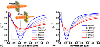
Finally, we apply these concepts to design a TPA-based nanoswitch, whose intensity-dependent nonlinear response may be used to modulate the intensity of transmitted light (i.e., resistive switching). Here we use the same nanocircuit in Fig. 1(b), with g 1 = 0.8 nm, g 2 = 5 w, and L = 8 nm. Figures 5(a) and 5(b) report the transmittance spectrum under various illumination intensities, for metal thickness h = 60 and 40 nm. The inset of Fig. 5(b) illustrates the onset and offset of such device, realized with the variation of input intensity. By increasing the incident irradiance, the transmittance can be largely modulated, due to the enhanced TPA effects and its enabled nonlinear self-modulation in the quantum resistance, Re[Z ox]. The inset of Fig. 5(b) illustrates the onset and offset of such device, realized by varying the input intensity. Under high-input intensities, the MOM nanojunction may absorb considerable power, leading to the deterioration of local field enhancement, as well as a variation in transparency and absorption. Moreover, the peak resonance with largest modulation depth can be readily tailored by designing the nanocircuit, as seen in Figs. 5(a) and 5(b). Unlike bistable switching devices based on reactive nonlinear responses (i.e., Re[χ (2)] or n 2),[ Reference Chen, Farhat and Alù 13 – Reference Maksymov, Miroshnichenko and Kivshar 21 , Reference Argyropoulos, Chen, D'Aguanno, Engheta and Alù 45 , Reference Argyropoulos, Chen, Monticone, D'Aguanno and Alù 46 ] this nonlinear resistive switching can offer significantly improved bandwidth, of interest for all-optical switching.
Transmittance spectrum for the metatronic circuit in Fig. 1(b), with metal thickness of (a) h = 60 nm and (b) h = 40 nm, under different illumination intensities.

In summary, we have introduced here nonlinear IR metatronic elements as building blocks for frequency and amplitude modulation, analogous to RF diodes, despite their nanosize feature. In this work, we focused on second-harmonic generation [which shows a high equivalent χ (2) of 1.8 × 10⁴ pm/V] and broadband self-amplitude modulation of transmittance via nonlinear two-photon absorption. These devices were designed and analyzed using the circuit concept, and they may be applied to novel IR mixers, transponders, and switches. We envision that the enhanced optical nonlinearities due to the interplay between PAT and plasmon coupling within atomic-scale MOM-superlattices, common in metamaterial and metatronic-circuit topologies,[ Reference Sun, Edwards, Alù and Engheta 3 , Reference Caglayan, Hong, Edwards, Kagan and Engheta 4 ] may provide tremendous potential in the design of novel nonlinear nanophotonic and nano-optical devices.
Supplementary materials
For supplementary material for this article, please visit http://dx.doi.org/10.1557/mrc.2015.75
Acknowledgments
A.A. acknowledges support from the Air Force Office of Scientific Research with grant No. FA9550-13-1-0204, and the Office of Naval Research with MURI grant No. N00014-10-1-0942.