Introduction
Nanostructured devices with more exciting properties and performance capabilities continue to be discovered.Reference Law, Goldberger and Yang1 Yet, to make these devices commercially viable requires significant improvement both in fundamental understanding and technological innovation. The theme of this MRS Bulletin issue, contact materials, is no less important for nanowire devices and nanoelectromechanical switches than any of the other types of nanoelectronic devices. Due to their exceedingly small size, nanoscale devices present severe challenges in terms of contact resistance (see Equation 1 in the introductory article). For bulk materials, the ideal barrier could be theoretically described by ϕB = ϕM – χs, where ϕM is the work function of metal, and χs is the electron affinity of a semiconductor. In reality, the theoretical barrier heights are hardly ever achieved mainly due to interfacial effects, such as the well-known Fermi-level pinning effect.Reference Allen2 Fermi-level pinning can be explained by the metal-induced gap states theory, a quantum mechanics–based theory where the interface of metal and semiconductor adds a boundary condition to the Schrödinger’s equation that describes the bandgap in semiconductors. The solutions are energy states that exist inside the bandgap of the semiconductor that can potentially pin the Fermi level. Achieving low resistance contacts hence requires that the Fermi-level pinning is mitigated.
Contacts to nanowires
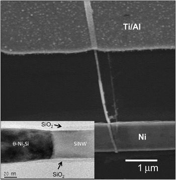
Si nanowire devices are interesting because they stand to benefit from the vast existing Si industry experience, and, in fact, silicon nanowires have been made by many methods.Reference Schmidt, Wittemann, Senz and Gösele3 The large surface area-to-volume ratio and exceedingly small size make it harder to obtain Si nanowire devices with the desired ohmic contacts or appropriate barrier heights compared to bulk Si. This is because of several issues such as nanowire size fluctuations, which can affect bandgap and barrier heights, especially for ultra-scaled (sub-20 nm diameter) nanowires;Reference Landman, Barnett, Scherbakov and Avouris4, Reference Leonard and Talin5 dopant fluctuations, where a dopant concentration difference of only a few atoms significantly alters the interface and wire size, affecting the bandgap;Reference Hanrath and Korgel6 and surface states that have been observed in Si nanowires covered with thermal oxides.Reference Piscator and Engström7, Reference Seo, Sharma, Yasseri, Stewart and Kamins8 Despite these challenges, some nice work has been shown recently on single nanowire devices. For example, Woodruff et al. fabricated Si nanowire diodes with Ni and Ni2Si contacts on n-type Si. They demonstrated ohmic contacts with Ni by heavily doping the Si nanowire and 0.69 eV barrier heights with Ni2Si, which is similar to bulk Si barrier height valuesReference Woodruff, Dellas, Liu, Eichfeld, Mayer, Redwing and Mohney9 (see Figure 1). Other reports have shown that ohmic contacts to Si nanowires can be achieved, for example, with Al/Au contacts.Reference Tans, Verschueren and Dekker10 So it appears that, in principle, ohmic contacts to single Si nanowires can be made.
Contacts between a Si nanowire and Ni and Ni2Si contacts.Reference Schmidt, Wittemann, Senz and Gösele3

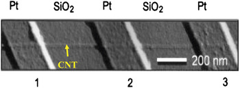
Carbon nanotubes (CNTs) offer exceptional mobilities that make them attractive for nanodevice applications. One key issue with CNTs is that they tend to have a Schottky barrier at the CNT/contact interface, which severely limits device performance.Reference Anantram and Leonard11 The low dimensionality of the tubes and electrode geometry can contribute to this barrier formation. In addition, nanotube size fluctuations may lead to variation in the barrier height, as semiconducting CNTs have a diameter-dependent energy gap that roughly scales as 0.9 eV/d (nm), where d is the diameter of the CNT.Reference McEuen, Fuhrer and Park12 Thus, designing a contact material to obtain a desired barrier height will likely be difficult if CNT diameters are not tightly controlled. A CNT field-effect device with Pt contacts was demonstrated in 1998 by making three Pt metal contacts on one single-wall CNT,Reference Heinze, Tersoff, Martel, Derycke, Appenzeller and Avouris13 which is a semiconducting-type CNT. In Figure 2, the atomic force microscopy tapping mode image of the device is shown. According to the literature, the semiconducting CNT has a work function of 4.5 eV, while the work function of Pt is 5.7 eV. Consequently, the contact forms a Schottky barrier. Approaches to realize ohmic contacts on CNTs include using contacts with a work function larger than 4.8 eV or less than 4.2 eV, H2 treatment (the Schottky barrier between metal contacts and the semiconducting CNT can be tuned by modifying the electrodes’ work function by hydrogen treatment),Reference Javey, Guo, Wang, Lundstrom and Dai14 vacuum anneal, and post-contact deposition anneal to desorb oxygen; all can help achieve a smaller barrier.Reference McEuen, Fuhrer and Park12, Reference Derycke, Martel, Appenzeller and Avouris15
Atomic force microscopy tapping mode image of a carbon nanotube-based field-effect transistor. The numbers 1, 2, and 3 correspond to the three contacts: source, drain, and gate.Reference Landman, Barnett, Scherbakov and Avouris4

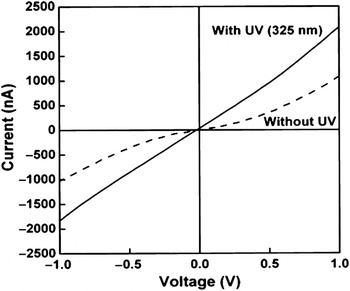
Devices based on other nanowire materials have been fabricated and have shown interesting effects. A systematic study on the contact in GaN nanowire devices was carried out by a group in Korea in 2006.Reference Ham, Choi, Hwang, Park, Lee and Myoung16 The single-crystalline GaN nanowires were synthesized by thermal evaporation and were randomly dispersed on a p-type Si substrate, which has a 100-nm-thick SiO2 layer. The source and drain electrodes were fabricated by sputtering Ti/Au. The source-drain I-V behavior was nonlinear, indicating non-ohmic behavior (Figure 3 dotted line). When the GaN nanowire device was illuminated with ultraviolet (UV) light, which has a photon energy larger than the nanowire’s bandgap energy, the current-voltage curve changed to linear behavior, as shown in Figure 3 (solid line), indicating that ohmic contacts were formed by introducing UV illumination. The possible reason for this behavior is that the UV illumination produced excess electrons moving to a different energy state in the nanowires, which narrowed the depletion region near the contact and formed a tunneling channel.
Current-voltage (I-V) characteristics of a GaN nanowire device in the dark and under ultraviolet (UV) illumination.Reference Ham, Choi, Hwang, Park, Lee and Myoung16

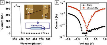
Different research groups have studied the contact between ZnO nanowires and metal, and the barrier height showed contact material dependence.Reference Zhou, Gu, Hu, Mai, Yeh, Bao, Sood, Polla and Wang17, Reference Wei, Yeh, Lu and Wang18 Ohmic contacts formed when ZnO nanowires with Ti/Au electrodes were used.Reference Wei, Yeh, Lu and Wang18 When the ZnO nanowire device was fabricated with Pt and Pt:Ga electrodes, Schottky contacts formed at the ZnO nanowire/Pt interface (Figure 4). The ZnO oxide I-V characteristics were changed using UV light (Figure 4b), indicating the possibility of using the nanowire as a UV detector.
(a) Current-voltage (I-V) characteristics of a ZnO nanowire device. Inset is a scanning electron microscopy image of the UV-detecting device made of a ZnO nanowire (black line connecting the Pt:Ga and Pt components). A schematic of the electronic circuit is also included as an inset. (b) The I-V curves of the device with and without UV illumination.Reference Wei, Yeh, Lu and Wang18

Contact engineering for nanoelectromechanical switches
Another type of nanoscale device being addressed here is the nanoelectromechanical switching device. These devices will present a different set of challenges, besides the common issues of contact resistance and barrier height seen with nanowire devices. These challenges include the requirement of low stress contacts and mechanical integrity of the contact interface with the active materials, particularly for the moving parts. With the physical scaling of advanced CMOS devices, the smaller dimensions of nanoelectromechanical (NEM) switches offer exciting opportunities, such as higher sensitivity, greater energy efficiency, and rapid switching, as well as a scaling benefit from the perspective of parallel data processing (multiple logic operations with one switching action). However, to ensure optimal performance, appropriate device architecture, advanced materials, and fabrication are required for their successful integration. In charge transport, especially in electron-based semiconductor devices, thermal voltage (k BT/q), where k B = Boltzman’s constant, T = temperature, and q = charge, is not scalable, therefore limiting the scaling of the metal oxide semiconductor field-effect transistor (MOSFET) threshold voltage (V t) and operating voltage (V dd). To overcome this limit, alternative switching device designsReference Gopalakrishnan, Griffin and Plummer19, Reference Choi, Park, Lee and Liu20 that can achieve a less than 60 mV/decade subthreshold swing (SS) have been proposed and demonstrated. However, many of these devices fail to maintain the improved I on/I off across a range of V dd values.
At the 2008 International Electron Devices Meeting, Kam et al. reported that dynamic energy can be reduced quadratically by decreasing V dd, but to avoid an increased circuit delay, V t must be decreased together with V dd to maintain a high on-state drive current (I on).Reference Kam, Liu, Alon and Horowitz21 Based on this analysis, if NEM switches can be fabricated with low surface forces and operated reliably over trillions of cycles, relay technology could improve energy efficiency dramatically over a wider range of performance.
To supplement this, Akarvardar et al.22 reported that the idea of combining an electrostatically actuated mechanical switch with a MOSFET was first introduced 40 years ago.Reference Akarvardar, Eggimann, Tsamados, Chauhan, Wan, Ionescu, Howe and Wong23 Hybrid microelectromechanical system (MEMS)/field-effect transistor (FET) structures were mainly used in gasReference Nathanson, Newell and Wickstrom24–Reference Gergintschew, Kornetzky and Schipanski27 and pressure sensing.Reference Voorthuyzen and Bergveld28, Reference Huang, Howe and Lee29 Subsequently, the suspended gate FET (SGFET), a variant of the resonant-gate FET, was conceived as an abrupt current switch:Reference Ionescu, Pott, Fritschi, Banerjee, Declercq, Renaud, Hibert, Fluckiger and Racine30 dynamic threshold operation and the possibility of a sub-threshold swing below the 60 mV/decade limit were reported. Recently, the accumulation-mode SGFET was introduced as a promising device for high-performance logic circuits.Reference Kam, Lee, Howe and King31 It is shown that such a structure, in theory, can meet performance specifications in the International Technology Roadmap for Semiconductors for low power applications at a 25 nm gate length.22
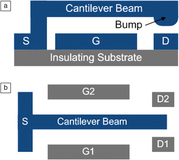
Two major design rules are currently competing to deliver the ultimate performance requirement. The first is based on a conventional vertically actuated cantilever that utilizes an accumulation-mode design. This design, has an operation state in which attraction between the polarity of pull-in (actuation) voltage and the minority charges create a channel to enhance performance characteristics (Figure 5a).22 The gate electrode is assumed to be anchored on either side of the channel (in/out of the plane of the figure), thus forming a clamped-clamped beam (with a characteristic spring constant k) suspended over the channel. In the off state (gate voltage V g = 0 V), the gate electrode is pulled down (so that it contacts the thin gate dielectric) due to the work function difference (ΦMS) between the gate and the channel, which results in an attractive electrostatic force. The channel region is therefore fully depleted in the off state. Capacitive coupling between the gate and the channel is therefore maximized to suppress short-channel effects, and the device is in a high-V T state. As V g is increased, the depletion depth in the channel decreases, and hence more current can flow between the source and drain regions. V g also serves to counteract ΦMS to reduce the attractive electrostatic force between the gate and the channel. At a critical release voltage V pull-out (for which the electrostatic force equals the spring-restoring force of the gate), the gate abruptly pulls away from the channel. As a result, the depletion depth decreases, the channel current increases abruptly at V g = V on, and the device enters a low V T state.
Architecture of conventional nanoelectromechanical systems (NEMS): (a) Profile view of vertically actuated NEMS, where the deflection is in the out-of-plane direction. (b) Top view of a laterally actuated NEMS with two actuation electrodes to implement a two-state switch. S, G, and D are source, gate, and drain, respectively.

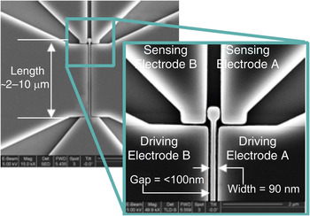
In contrast to the vertically actuated cantilever-based NEM switch, Akarvardar et al.Reference Akarvardar, Elata, Parsa, Wan, Yoo, Provine, Peumans, Howe and Wong32 introduced laterally actuated energy-reversible complementary nanoelectromechanical (ER CNEM) logic gates (Figure 5b). This design is like a pendulum. While moving toward one end with a biasing voltage (pull-in voltage) applied, the switch (cantilever) gathers potential energy. Because it behaves like a spring, after release from that end, the cantilever automatically starts moving toward the opposite direction. But now the motion is happening even without the application of a pull-in voltage on the other side. If appropriately designed, the cantilever can get close to, or even touch, the opposite end, thus reducing the pull-in voltage if applied from the other side. So, for the same delay, ER CNEM gates can operate at much lower supply voltages than conventional (CMOS-like) CNEM gates, and their reliability is significantly higher.
Contact materials for nanoelectromechanical devices
Usually MEMS and NEMS devices have unique structural characteristics, because they move mechanically under electric bias and then touch a specific sensor contact material at the end of the motion. Therefore, material choice and contact engineering are important factors in the successful fabrication of NEM switches. Conventional silicon and poly-SiGe materials are more popular in the MEMS world. However, in the nanoscale, these materials may pose a significant challenge, as their grain size and stress become dominating factors in defining their characteristics. To address these challenges, researchers such as Singh et al. have demonstrated a nanoscale electromechanical actuator device using an isolated nanoscale spring.Reference Singh, Liu, Ye, Picu, Lu and Wang33 The four-turn Si nanosprings were grown using the oblique angle deposition technique with substrate rotation; they were rendered conductive by a 10-nm-thick Co layer applied using chemical vapor deposition. Bargatin et al. observed resonances from multiple vibrational modes of individual silicon-carbide-based nanomechanical resonators, covering a broad frequency range from several megahertz to over a gigahertz.Reference Bargatin, Kozinsky and Roukes34 Jang et al. developed a titanium nitride (TiN)-based NEM switch using “top-down” CMOS fabrication methods. A cantilever-type NEM switch with a 15-nm-thick suspension air gap and a 35-nm-thick TiN beam was successfully fabricated and characterized.Reference Jang, Lee, Yoon, Kim, Lee, Kim, Cho, Kim, Park and Lee35 It showed an essentially zero off current, an abrupt switching with less than 3 mV/decade, and an on/off current ratio exceeding 105 in ambient air. Yamaguchi et al. demonstrated applying the self-organization growth technique to the fabrication of nanoscale mechanical structures.Reference Yousif, Lundgren, Ghavanini, Enoksson and Bengtsson37 They selectively etched a GaAs sacrificial layer under InAs wires preferentially grown in bunched steps on misoriented GaAs (110) surfaces, which led to the formation of single-crystal InAs nanoscale cantilevers.
An excellent choice of material for NEM switches would be an amorphous metal with a slightly tensile stress to induce an upward buckling of the structural material, thus giving it an extra degree of freedom so it will not fall down onto the contact pad. There is also increased interest in carbon-based materials such as CNTs or graphene. Based on a simulation to achieve a few volts of switching, the gap between the structural material and the contact needs to be in the sub-10 nm region.Reference Akarvardar and Wong36 Therefore, CNT or graphene seems to be a very reasonable choice. Based on inserting one-dimensional structure CNTs, nanowires, and molecular devices into an otherwise Si platform, several devices with the potential to boost CMOS circuit performance have been realized.Reference Yousif, Lundgren, Ghavanini, Enoksson and Bengtsson37–Reference Ilani, Donev, Kindermann and McEuen44 Despite extensive research on CNTs since their discovery, several issues still need to be resolved. The most important of these is better reproducibility of the desired CNTs. Control over the CNT type (metallic or semiconducting), chirality, diameter, and placement in desired positions remains challenging.Reference Rebeiz and Muldavin45 Bunch et al. have fabricated NEM systems from single- and multilayer graphene sheets by mechanically exfoliating thin sheets from graphite over trenches in silicon oxide.Reference Bunch, Zande, Verbridge, Frank, Tanenbaum, Parpia, Craighead and McEuen46 Appropriate contact material (metal with a higher modulus than poly-Si; therefore, the modulus of a composite beam will have a higher modulus than that of a poly-Si only beam) may increase stiffness in the NEM switches to achieve faster switching. Also, utilization of a metallic contact mitigates the oxide growth issue on a poly-Si or crystalline Si beam sidewall. Higher switching frequency (f switching) was observed with the metallic contact than the simulated value for a poly-Si switch of this length. A metallic contact increases stiffness, modifies the quality factor (Q), and thus increases f switching, but at higher pull-in voltage, V pi (a voltage applied to move the switch to one end). In the recent past, we have demonstrated an amorphous metal-based vertical metallic contactReference Hussain, Smith, Elata, Akarvardar, Parsa, Yoo, Provine, Williams, Rader, Barnett, Park, Cruz, Kirsch, Wong, Howe and Jammy47 (Figure 6) where a metallic film has been used to form the sidewall. Another demonstration uses a Pt-based metallic contact to reduce the contact resistance significantly.Reference Parsa, Chong, Patil, Akarvardar, Provine, Lee, Elata, Mitra, Wong and Howe48
Sub-100 nm lateral nanoelectromechanical switch with vertical metallic contact on the sidewalls based on a state-of-the-art complementary metal oxide semiconductor-compatible flow.Reference Bunch, Zande, Verbridge, Frank, Tanenbaum, Parpia, Craighead and McEuen46

NEM switches are making progress in many arenas. Low-speed switches have applications in reconfigurable circuits and power management. Intermediate speed switches may be useful for static and nonvolatile memory. Finally, high-speed NEM switches are promising for logic circuitry by hybridization with classical MOSFET devices. Although NEM switches offer zero standby power consumption because of their discontinuity with the contact, resulting in zero leakage current, their main limitation is switching speed because of mechanical motion-based switching. To successfully fabricate a NEM switch, structures must be compensated for residual and thermal stress (average and gradient), making symmetric structures preferable to cantilevers or membranes. Deformable structures must be made from amorphous or single crystalline materials (to avoid grain-size effectsReference Javey, Guo, Wang, Lundstrom and Dai14). Conduction at the nanoscale must be better understood to improve the design. In macroscopic relays, where free particles have no effect, the dynamic electrode “scratches” the static electrode. This abrasive contact in NEMS is not an option. In test devices, switches are loaded through pads that have huge parasitic capacitance; therefore, the switches drain the uncontrolled current upon contact. In actual devices, this capacitance will be lower. Radio frequency ohmic switches that were tested in air (even with N2 purge) failed due to polymerization of organic molecules on the contacting electrodes.Reference Anantram and Leonard11 This failure mechanism turns ohmic switches into capacitive switches.
Hermetic packaging of test devices seems to be crucial. Casimir (a small attractive force that acts between two close parallel uncharged conducting plates, due to quantum vacuum fluctuations of the electromagnetic field) and van der Waals surface interaction forces must be better modeled and characterized with test structures having a gap between 2 and 15 nm (to calibrate the effects of finite conductivity and surface roughness). Surface interaction forces may be used to increase contact force and latch the switch in contact (turning the switch into non-volatile memory).
To move toward satisfying the criteria of choice of structural and contact material (preferably amorphous and slightly tensile), narrow gap formation, and appropriate sealing, lab-based demonstrations need to achieve reliable repeatability in fabrication and performance. Thus, choice of the right design and suitable contact material hold paramount importance.
Conclusion
Nanowire devices and nanoelectromechanical switches are emerging nanoelectronic devices. Their dimension scale is within the favor of integrating billions of them to add more functionality to integrated circuits. At the same time, this size reduction enables them to offer unique properties. Nonetheless, to fabricate them, many engineering challenges need to be overcome, and contact engineering is one of them. Choosing the appropriate contact materials, compatibility of their deposition processes, and acceptable minimized sheet resistance, which is contrary to its increment because of size decrement, all play critical roles and open up opportunities for researchers.