Introduction
The first focused ion beam (FIB) tools were built with the intent of direct-write milling and to expose resist, Reference Kanaya, Kawakatsu, Matsui and Yamazaki1–Reference Hill3 later evolving into an analytical tool as is mostly used today. Since then, FIB usage has exploded into a myriad of applications. A focused ion beam tool consists of an ion source that is at a voltage relative to ground, where the ions are accelerated down a tubular section that contains electrostatic optics used to focus and steer the beam of ions onto a sample in a chamber. The entire time the ions and sample are kept under high vacuum that can range from 10–9 Torr to 10–6 Torr. The reason for the high vacuum is to allow the ions to reach the sample without scattering off any other gas atoms that may get in the way. For a review on the wide range of ion beam micromachining applications, see the 2007 issue of MRS Bulletin, Reference Volkert and Minor4 the article by Allen, Reference Allen, Shore, Evans, Fanara, O’Brien, Marson and O’Neill5 and the Introductory article in this issue.
This article discusses three main areas of advancement in ion beam direct-write technology: ion beam lithography and micromachining, gas-assisted etching applications, and novel ion sources and applications.
Ion beam lithography and micromachining
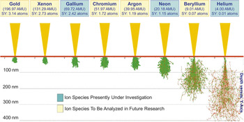
Direct-write ion beam lithography (DWIBL) started as an alternative to electron beam lithography, exposing polymer films, known as resists, to ions in the keV Reference Gamo and Namba6 or MeV energy range. Reference van Kan, Sanchez, Xu, Osipowicz and Watt7 The key feature highlighted by resist-based ion beam lithography is the relatively limited ion scattering when compared to electron scattering in electron beam lithography. Recent work on multiple ion sources shows that the scattering limit is only a few nanometers, see Figure 1 . Reference Tan, Livengood, Shima, Notte and McVey8 Resist-based lithography further evolved to projection ion beam lithography, where stencil masks and sophisticated projection optics were used to increase exposure throughput. Reference Selinger9,Reference Löschner, Stengl, Chalupka, Fegerl, Fischer, Hammel, Lammer, Malek, Nowak, Traher, Vonach, Wolf and Hill10 Most DWIBL work was performed using either a scanning beam or an ion projection approach, almost always based on Ga+ ion sources except for a few studies involving lighter ions such as H+, H2 +, Be+, and He+, as reviewed in articles by Melngailis et al. Reference Melngailis11,Reference Melngailis, Mondelli, Berry and Mohondro12
Modeled sputter yield, interaction volume, and implant depth of He+, Be+, Ne+, Ar+, Cr+, Ga+, Xe+, and Au+ at 30 keV beam energies in a silicon substrate. Throughout this figure, the incident ions are shown in red, and green is used to represent the dislocated silicon atoms. Reprinted with permission from Reference 8. © 2010 American Vacuum Society.

Modern FIB/SEM dual beam systems successfully combine the capabilities of particle beams into a powerful tool used for sample modification, analysis, and characterization. Depending on the dwell time, or the dose, direct-write lithography on a sample can be divided into surface/bulk amorphization (low dose) and direct milling (high dose). Recent work at low doses has been shown to lead to the intermixing of substrate target atoms. One of the most exciting new areas where this is being used is in changing material properties such that the target becomes etch resistant to chemicals that would normally etch the native untouched material such as the intermixing effect of Gallium on silicon or diamond. Reference Henry, Shearn, Chhim and Scherer13–Reference Tripathi, Scanlan, O’Hara, Nadzeyka, Bauerdick, Peto and Cross15 Intermixing can also enable etching in a preferential manner in H-Si <111> Reference Hildreth, Rykaczewski and Wong16 or induce a phase transition from conductor to insulator in ultrathin YBCO nanowires. Reference Curtz, Koller, Zbinden, Decroux, Antognazza, Fischer and Gisin17 These applications are much faster than traditional milling, as they require a fraction of the incident ions needed for material removal.
Ion beam micromachining (IBµM) is akin to electron beam lithography, where a beam of charged particles is steered by computer controlled electrostatic deflectors to draw structures contained in a computer-aided design (CAD) file. Unlike electron beam lithography, arbitrary depths can be programmed in the CAD file by manipulating the dwell time, dose, or multiple exposure passes Reference Nadzeyka, Peto, Bauerdick, Mayer, Keskinbora, Grévent, Weigand, Hirscher and Schütz18–Reference Ocola and Palacios21 for a particular structure. The reason is that the longer or more frequently the ions strike a sample, the more material is removed. Combining electron beam lithography techniques and high precision stages enable IBµM field stitching to cover millimeter scale areas. Reference Nadzeyka, Peto, Bauerdick, Mayer, Keskinbora, Grévent, Weigand, Hirscher and Schütz18,Reference Imre, Ocola, Rich and Klingfus19 This allows milling structures many times the size of a single field of view.
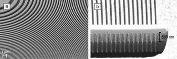
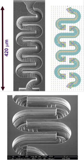
To achieve beam control close to that found in electron beam lithography tools, improvement of beam control is needed for large-area, high aspect ratio, nanoscale milling. Recent work using beam drift compensation with an interferometric stage based tool (a known solution in electron beam lithography tools) has shown unprecedented high aspect ratio milling of nanoscale structures, such as 100 nm Fresnel zone plates in gold, Figure 2 . Reference Nadzeyka, Peto, Bauerdick, Mayer, Keskinbora, Grévent, Weigand, Hirscher and Schütz18 An example of large-area direct-write IBµM used as a means to fabricate key components of a microfluidic device with complex geometries such as serpentine 3D mixers Reference Ocola and Palacios21 is shown in Figure 3 .
SEM micrographs showing a 45° tilted view of the zone plate: (a) inner zones and (b) 100 nm wide outer zones and cross-sectional view of the outermost zones. A tungsten protective layer on top was produced by ion beam induced deposition. The vertical stripes in the membrane are caused by curtaining effects during the ion beam cross-section cut. Reprinted with permission from Reference 18. © 2012 Elsevier.

Views of a 3D microfluidic serpentine mixer and computer-aided design data used for making the mixer. Reprinted with permission from Reference 21. © 2013 American Vacuum Society.

Therefore an ideal IBµM tool would have high current source, fast deflectors, a lithography interface with all the calibration routines found in an electron beam lithography tool, and an interferometric stage. Such a tool would enable a myriad of applications where standard lithography and etch processes cannot perform, and 3D IBµM can be used to create molds that could be readily replicated.
High resolution gas-assisted etching
In addition to simple mechanical sputtering, ion and electron beam processing can be performed in the presence of a precursor gas, which is usually introduced into the FIB sample chamber by a small diameter needle positioned close to the sample surface. This process is often referred to as gas-assisted etching (GAE). Reference Utke, Hoffmann and Melngailis22 During GAE, energy from the ion beam causes decomposition of the adsorbed precursor molecules, leading to localized chemical reactions that assist in material removal or result in net deposition of material, depending on the precursor molecule. Many gas precursors have been examined. Reference Utke, Hoffmann and Melngailis22
During GAE, the material removal is assisted by the formation of volatile by-products, which can then be pumped away from the vacuum chamber. An example is Equation 1:
 $${\rm{Si}}{{\rm{O}}_{\rm{2}}}\left( {\rm{s}} \right)\, + \,2{\rm{Xe}}{{\rm{F}}_{\rm{2}}}\left( {\rm{g}} \right)\, \to \,{\rm{Si}}{{\rm{F}}_{\rm{4}}}\left( {\rm{g}} \right)\, + \,{{\rm{O}}_{\rm{2}}}\left( {\rm{g}} \right){\rm{2Xe}}\left( {\rm{g}} \right).$$
The efficiency of FIB-based GAE is influenced by many different parameters, including dwell time, pixel spacing, refresh time, ion energy, current density, and, of course, the nature of the substrate and etching gases. Reference Herschbein, Fischer, Kane, Tenney and Shore23 The trends associated with GAE for medium to large pattern areas (from a few to hundreds of μm2) are reasonably well-understood and have been documented by various researchers. Reference Lipp, Frey, Franz, Demm, Petersen and Ryssel24–Reference Rue, Shepherd, Hallstein and Livengood29 However, GAE in very small pattern areas can be affected by the size and shape of the ion beam itself, and this size regime is relatively unexplored in the literature. Reference Utke, Hoffmann and Melngailis22,Reference Wu, Ferranti, Stern and Xia30–Reference Tan, Livengood, Greenzweig, Drezner and Shima32
One of today’s most demanding applications requiring high resolution GAE is the modification of integrated circuit devices (circuit edit), in which high-aspect ratio holes (commonly referred to as vias) with lateral dimensions on the order of 10s of nm need to be created by FIB milling. The milling resolution for straight sputtering applications (no gas) is limited by the physical size of the Ga+ ion beam and by the extended region of amorphous damage produced by the impact of the high-energy ions. Reference Tan, Livengood, Greenzweig, Drezner and Shima32 The minimum via size achievable with gas-assisted FIB milling also scales with beam current, but is typically larger than the footprint of the ion beam itself. It is clear that energy from the ion beam extends some finite distance away from the point of incidence and is capable of decomposing the gas precursor, leading to peripheral material removal. This extended zone of energy effectively raises the lower limit on gas-assisted milling resolution. Reference Tan, Livengood, Greenzweig, Drezner and Shima32
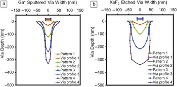
Recent work by Tan et al. Reference Tan, Livengood, Greenzweig, Drezner and Shima32 using small Ga+ beams (1.6 pA at 40 keV) achieved via sizes of approximately 100 nm on SiO2 substrates with XeF2 assisted FIB milling. Digitized and superimposed cross-sectional profiles of some of the vias from this work are reproduced in Figure 4 . The width of the patterned area (the drawn pattern size) was 25 nm in this work, so the excess lateral over-etch was approximately 75 nm. This result provides a tentative estimate of the smallest possible feature size for FIB GAE, but more studies are needed to define this limit with precision.
Digitized via width versus depth profiles for (a) sputtered and (b) XeF2 etched vias. All vias were patterned with 25 nm width. Patterns 1–4 received ion doses of 0.23, 0.90, 1.8, and 3.6 nC/μm, respectively, for series (a) and 0.028, 0.11, 0.22, and 0.43 nC/μm, respectively, for series (b). Reprinted with permission from Reference 32. © 2012 American Vacuum Society.

Cross-sectional analyses reveal differences in the relative shapes of vias created with and without GAE. Reference Tan, Livengood, Greenzweig, Drezner and Shima32 As shown in Figure 4, both sets of vias grow progressively deeper with increasing ion dose. However, note that the vias milled with XeF2-assist require significantly less dose to achieve the same depth as those milled without gas. Additionally, the tops of the vias milled without gas are generally more tapered and eroded, and the bottoms of the vias narrow to a tight constriction. In contrast, XeF2-assisted vias have relatively parallel and vertical sidewalls with wider openings at the bottom. Reference Tan, Livengood, Greenzweig, Drezner and Shima32 This effect difference in via shape becomes more pronounced with increasing depth. Compare via profile 4 in Figure 4a–b.
These differences can be explained with reference to the effects of Equation 1. Because the XeF2 assists in the volatilization and removal of the substrate material, redeposition effects are minimized, which alleviates the constriction at the bottom of the gas-assisted vias. Additionally, GAE allows a via to reach a desired target depth with less ion dose. This, in turn, minimizes exposure of the sample to interaction with the beam tails, which is responsible for the tapered opening at the top of the vias milled without gas. The combined result of these factors is that GAE allows vias to be created with a higher aspect ratio and a cleaner profile. Reference Tan, Livengood, Greenzweig, Drezner and Shima32
Direct-write applications of gas field ion sources
The realization of a practical gas field ionization source (GFIS) has enabled helium and neon ion microscopy (HIM and NIM) as new techniques to image and modify materials and microstructures. Reference Ward, Notte and Economou33–Reference Hill and Faridur Rahman35 The He GFIS has an ultrahigh brightness of 10–9 A cm–2 sr–1 V–1, is stable, and delivers sufficient beam current to ensure realistic image acquisition and pattern formation times. Reference Alkemade, Koster, van Veldhoven and Maas36 A key element in HIM applications is the ultra-local interaction of the helium beam with the target surface. In the first ten-to-hundred nm in the sample, incident He+ and Ne+ ions lose their energy through inelastic collisions. These collisions yield low energy (less than 20 eV) SEs with a short mean free path (less than 10 nm), without significant lateral scattering of the ion. As a result, the interaction is ultra-local (i.e., many secondary electrons and a few backscattered ions that are to a very high degree localized around the incidence point of the helium beam). This simple fact allows the helium ion microscope to enable a new and unique view of surfaces and provides a new method for material modification. Reference Sidorkin, van Veldhoven, van der Drift, Alkemade, Salemink and Maas37
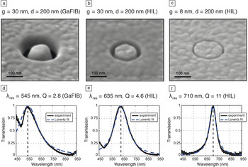
Despite intrinsic advantages of Ga+ DWIBL (described earlier), practical disadvantages such as lower resolution due to the larger ion spot size and, when using Ga+ ions, the risk of substrate damage or contamination from the ion impact, inhibited large-scale applications. The sub-nanometer sized He+ and Ne+ ion probes offered by the GFIS in the HIM address the resolution shortcoming, while capitalizing on the negligible proximity effect. Reference Maas, van der Drift, van Veldhoven, Meessen, Rudneva, Alkemade, Marletta, Öztarhan, Baglin and Ila38–Reference Melli, Polyakov, Gargas, Huynh, Scipioni, Bao, Ogletree, Schuck, Cabrini and Weber-Bargioni40 Figure 5 shows a direct comparison of Ga+ and He+ beam direct-write manufactured plasmonic structures in gold, including their spectral response. Only the nanoantennas made with He+ can reach the theoretical quality factor for resonant structures, since the required dimensions cannot be reached with Ga+ milling. Reference Livengood, Tan, Greenzweig, Notte and McVey41 Meanwhile, characterizing and preferably avoiding significant damage to the substrate while patterning is an active materials research topic. Reference Aramaki, Ogawa, Matsuda, Kozakai, Sugiyama, Obaa, Yasaka, Amano, Shigemura and Suga42–Reference Drezner, Greenzweig, Fishman, van Veldhoven, Maas, Raveh and Livengood45
(a−c) SEM images of coaxial apertures with a 200 nm diameter in a 100-nm-thick gold film. (a) Coax made with Ga-DWIBL with a nominal gap of 30 nm. (b–c) Coax made with He-DWIBL with a nominal gap of 30 nm and 8 nm, respectively. (d−f) Corresponding transmission spectra. Reprinted with permission from Reference 41. © 2013 American Chemical Society.

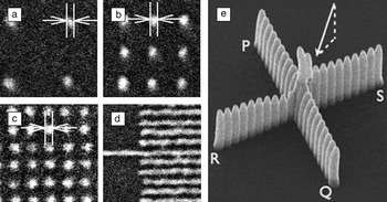
The Orion Plus HIM (Carl Zeiss) is a FIB system that can be used for nanopatterning on silicon, either by scanning helium ion beam lithography (SHIBL) using hydrogen silsesquioxane resist or using helium ion beam induced deposition (HIBID) using a Pt-precursor gas (MeCpPt(Me3)) from a gas injection system. Figure 6 a–d shows SEM images of dots and lines as patterned in HSQ resist on a Si wafer (75 nm field of view) that demonstrate the ultra/low proximity of SHIBL. The pitch-independent dot size (Figure 6a–c) is 6 nm (spacing between arrows). Reference Maas, van der Drift, van Veldhoven, Meessen, Rudneva, Alkemade, Marletta, Öztarhan, Baglin and Ila38 Isolated lines, and lines and spaces (Figure 6d) print at the same dose at 5 nm half pitch. Reference Li, Wu and Williams39 Figure 6e shows a Pt HIBID cross formed by two successively grown rows of 21 pillars at 75-nm separation. Row PQ was grown first. The arrow indicates the flow direction of the MeCPPt(Me)3 precursor. Every pillar was grown by repeated point exposures of 50 μs, enabling the depleted precursor layer to replenish during the exposure of the other pillars. Since for helium, the sputter rate is much lower than for gallium while the deposition yield per ion is similar, the shape of the pillar top reflects the interaction range of helium in the deposited material. Most Pt-HIBID deposits consist of 20% Pt and ∼80% carbohydrates reflecting the composition of the dissociated MeCPPt(Me)3 precursor, which contains carbon and hydrogen, Reference Chen, Van Veldhoven, Sanford, Salemink, Maas, Smith, Rack and Alkemade31 although up to 40% Pt has been reported for HIBID.45 The obtainable resolution is now limited by the interaction range of the secondary electrons in the target material. The differences between rows PQ and RS show the importance of optimizing and control over the beam scan routine over the substrate. Reference Sidorkin, van Veldhoven, van der Drift, Alkemade, Salemink and Maas37
(a–d) Examples of scanning helium ion beam lithography in 5-nm-thick hydrogen silsesquioxane resist. Reprinted with permission from Reference 38. © 2011 Materials Research Society. (e) Pt helium ion beam-induced deposition. Reprinted with permission from Reference 37. © 2009 American Vacuum Society.

Several studies on various GFIS-based instruments have shown that HIM and NIM have the ability to image and produce fine and dense features. Typically, the best precision achieved in nanofabrication with a GFIS-based FIB lies between 5 and 10 nm.
Summary
High-resolution direct-write patterning using focused ion beams is still a very active area of research expanding into novel areas where detailed control can lead novel structures ranging from nanometer-scale to micron-scale dimensions. The advent of gas assistance and novel ion sources further expand the realm of application possibilities. It is clear that direct-write ion beam tools will evolve as demand for new applications pushes the limits of ion beam direct write.
Acknowledgments
This work was performed, in part, at the Argonne National Laboratory Center for Nanoscale Materials, US Department of Energy, Office of Science, Office of Basic Energy Sciences User Facility under Contract No. DE-AC02–06CH11357. Part of this work is also supported by NanoNextNL, a micro and nanotechnology consortium of the Government of the Netherlands and 130 partners. D.M. acknowledges Paul F.A. Alkemade for his essential contribution to developing nanofabrication techniques with the HIM.