Introduction
In stealth technology, absorbing materials are primarily used to convert electromagnetic (EM) energy into other forms such as, heat or weaken them through interference cancellation that leads to RCS reduction. The conventional EM absorbers can be categorized into two types, i.e.absorbing material [Reference X, H and Y1, Reference C, Y, XL, CX and L2] and absorbing structures [Reference Cheng, Yang, Cheng and Wu3–Reference Li, Yang and Hou6]. In the literature, many studies have been carried out to study the EM response of metamaterials (MMs) or metasurfaces (MSs) and their implementations in the area of sensing [Reference Du, Tan and Xing7], cloaking [Reference Pendry, Schurig and Smith8], waveguide [Reference Yamamoto and Nomura9], absorber [Reference Cheng, Yang, Cheng and Wu3–Reference Li, Yang and Hou6], reflection [Reference Kanchana, Radha, Sreeja and Manikandan10, Reference Yuan, Zhao and Xi11], polarization conversion [Reference Akram, Mehmood, Tauqeer, Rana, Rukhlenko and Zhu12–Reference Akram, Bai, Jin, Vandenbosch, Premaratne and Zhu14] and checkerboard artificial magnetic conductor [Reference Yuan, Xu, Jia, Wang and Fu15, Reference Sang, Chen, Sang, Chen, Ding, Guo and Fu16]. However, almost all reported structures were limited to a single function. Over the past few years, MMs have been employed to miniaturized and compact antennas, such as complementary split-ring resonator (CSRR) loaded antenna [Reference Sharawi, Khan, Numan and Aloi17, Reference Limaye and Venkataraman18], slotted CSRR [Reference Bait-Suwailam and AI-Rizzo19] and artificial magnetic materials with fractal Hilbert inclusions [Reference Yousefi and Ramahi20]. Moreover, MMs have been employed as an effective medium to improve the gain of conventional antennas [Reference Attia, Yousefi, Bait-Suwailam, Boybay and Ramahi21] and directivity [Reference Wu, Wang, Pacheco, Chen, Lu, Grzegorczyk, Kong, Kao, Theophelakes and Hogan22] rather than consider it as the main radiators. The MS-based antennas were proposed earlier to construct small antennas by miniaturizing the antenna size [Reference Ziolkowski and Erentok23, Reference Erentok and Ziolkowski24].
Recently, many researchers have tried to achieve multifunctionality using the same MM inspired structures [Reference Sheng, Ge, Han and Zhu25–Reference Li, Li, Wang, Wang and Cao33]. Frequency-selective surface (FSS) with transmission and reflection characteristics was proposed in [Reference Sheng, Ge, Han and Zhu25]. The reflection and transmission coefficients were achieved at two different frequency bands with the transmission in X-band and reflection in Ku and Ka bands. Although, the same surface has been used for both transmission and reflection, within different frequency bands. In [Reference Agarwal and Prajapati26], a multifunctional MS structure for two different applications, namely, absorber and sensor was proposed. It has been shown that the MS achieves good absorbance in the range of 100–500 nm (in wavelength). Further, the same surface was utilized for sucrose detection using the surface plasmon resonance concept in the infrared region, which offers good detection accuracy and moderate sensitivity. Recently, FSS with transmission and scattering deflection based on spoof surface plasmon polariton modes was also investigated [Reference Wang, Yongfeng, Maochang, Jiafu, Hua, Jieqiu and Shaobo28]. The transmission and scattering deflection was achieved by using a reflection type coding MM of the metallic fishbone structure. Under linearly polarized wave normal incidence, the transmissivity of the FSS exceeds − 0.8 dB for the frequency below f = 9.5 GHz. In the stopband, the RCS reduction is higher than 10 dB from 14.4 to 18.0 GHz. In [Reference Bakshi, Member and Mitra29], a reconfigurable ra-sorber was proposed based on the switching activity of FSS. It has switchable transmission and reflection bands.
In [Reference Li, Cao, Liu and Wang30–Reference Li, Filippo, Junjie, Lili, Yi, Qunsheng and Agostino32], multi-functional FSSs were designed with different functions such are polarization selection, frequency tuning, and EM switching.
To the author's best knowledge, a multi-functional structure for different application, i.e. absorber and antenna have not been presented so far. However, in [Reference Li, Yi, Luo, Muneer and Zhu34, Reference Rahman, Cao, Gil, Sajjad and Wang35], the authors have tried to design absorber and antenna in an integrated form. But the integrated structure has a few limitations, e.g. lumped resistors were fixed in the antenna element that degrades the radiation characteristics. Moreover, the radiator has a narrow operating band and a bulky size with limited RCS reduction. Other researchers in this area mainly focuses on the combination of MS with regular patch antenna to reduce its RCS [Reference Baskey, Johari and Akhtar36–Reference Veluchamy, Mohammed, Krishnasamy and Jyoti46], e.g. a low RCS patch antenna based on MM absorber [Reference Baskey, Johari and Akhtar36, Reference Liu and Zhao38, Reference Liu, Li, Jia, Zhang and Zhou45], polarization conversion [Reference Li, Liu, Jia and Guo40, Reference Rahman, Qunsheng, Akram, Amin and Wang41], or EM bandgap [Reference Jang, Lee and Kim44]. In the mentioned designed structures, the MMs were designed separately and loaded to a regular patch antenna for RCS reduction. The traditional methods generally lead to gain degradation, narrow bandwidth, and bulky size. Also in [Reference Veluchamy, Mohammed, Krishnasamy and Jyoti46], a wideband and single-layer reflectarray antenna with cross loop and square ring slot loaded patch elements was designed. The designed reflectarray exhibits high gain and aperture efficiency. However, the designed reflectarray was limited to a single function. Moreover, the analytical study of the radiators was extensively carried out in [Reference Valagiannopoulos47, Reference Valagiannopoulos48].
In this research work, we present the integration of MS such as FSS and antennas that operates in the microwave regime. The proposed novel design exhibits multilayers that have two different functions within the same frequency band, i.e. EM absorption and radiation. The function EM absorption is dependent on the free space plane wave. When the p-i-n switches in the feeding network are switched off, i.e. that break down connection among resonators on top layer and feeding network bottom layer, then the resonators on the upper grounded substrate behave as an absorber for free space plane wave source. The absorber operates from 6.2 to 8.2 GHz and is polarization-insensitive over an incident angle of 0° to 30°. The operated p-i-n switches connect the feeding network and the disk-shaped patches for EM radiation and the same structure works as an EM radiator within the same absorbing frequency band with a high gain of 14.5 dB and minimum RCS of − 26.12 dB within the operating band. This research work provides an alternative approach to constructing a multi-functional structure with EM absorption and radiation functions and also to resolving the conflict among high gain and low RCS requirements.
Multifunctional circuit model
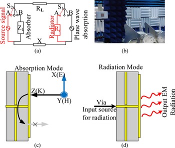
To demonstrate the idea of multi-functionality, the combined circuit model of the absorber and radiator is shown in Fig. 1. The transformation of the circuit model as an absorber or radiator is dependent on the single pole double throw switches. The multi-functional equivalent circuit model performs the functions, absorption, and radiation alternatively by selecting different states through suitable switches.
(a) Multifunctional circuit model of EM absorber/radiator, (b) experimental setup and operational modes of the proposed structure, (c) absorption, and (d) radiation mode.

Absorption mode
The multifunctional circuit model of the absorber/antenna is shown in Fig. 1. When switches “S 1”, “S 2”, and “B” are in contact, the circuit model transforms into the absorber's typical equivalent circuit model. The equivalent circuit theory is employed to analyze the characteristic of absorbing structures [Reference Costa, Monorchio and Manara52, Reference Li, Xiao, Bai and Wang53]. The equivalent input impedance of a typical single-port absorber can be defined as:

if the structure exhibits lumped components, i.e. resistors, capacitors, or inductors then (1) can be re-written as:

It should be noted that in equation (2), Z L represents the lumped components, and R L and jX represent the equivalent resistance and reactance caused by the absorbing structure and absorber's material. Therefore, the operation of an absorber is described in Figs 1(a) and 1(c), where the excitation is the incident-free space plane wave.
Radiation mode
The working principle and operation of the radiator are shown in Figs 1(a) and 1(d). To describe the multi-functional circuit model as the radiator's equivalent circuit model as shown in Fig. 1(a), the switches S 1 and S 2 have to be in-contact with “A” or the switches S 1 and S 2 are in-contact with some source signal. The input impedance of the antenna of a typical antenna can be written as:

In equation (3), R r represents radiation resistance, which shows the radiated power into the free space, R L is the loss resistance caused by diverse losses, X is the reactance of the antenna.
It should be noted that by selecting suitable Z L, the matching between free space and physical structure has to be preserved in both cases. Switch S 2 is required in the physical structure because operation as an absorber/antenna is only determined by switch S 1. In the physical structure, the switch S 2 is realized by embedding two p-i-n diodes. When the p-i-n diodes are switched ON, the disc shape patches are in contact with some input source signal for EM radiation.
Design and analysis
Design and analysis of the absorber
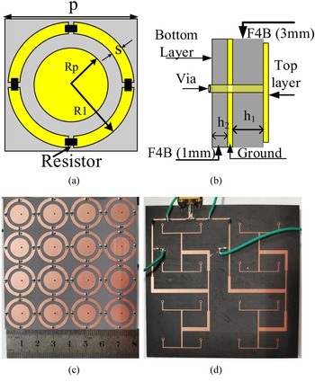
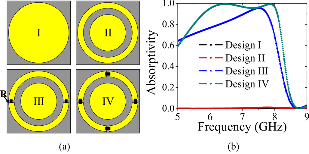
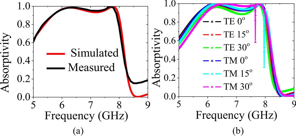
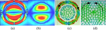
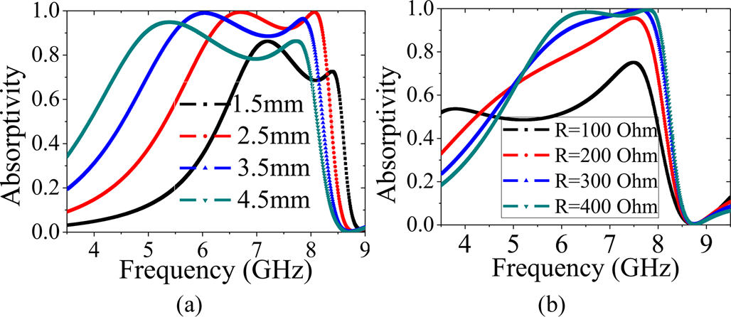
The schematic view of the designed unit cell is shown in Fig. 2. The unit cell is composed of multi-layers having two F4B substrates with a dielectric constant of 2.65. The resonator consists of a split-ring and disk-shaped patch. To obtain the favored operating frequency and optimized unit cell, a straightforward design of a ring patch has been designed and studied in [Reference Mat, Misran, Islam and Mansor54]. The optimized geometry of the unit cell as shown in Fig. 2(a) is determined as the periodicity p = 20.5 mm, split-ring width s = 0.5 mm, split ring radius R1 = 9.7 mm, and disk-shaped patch radius Rp = 5.7 mm, where the thickness of the upper substrate is h1 = 3 mm and lower substrate h2 = 1 mm. The lumped resistors with resistances equal to 470 Ω are embedded in the split ring to enhance the absorption rate. The simulations were performed by CST Microwave Studio using floquet port excitation. The schematic view of the experimental setup is displayed in Fig. 1(b). In Fig. 1(b), one horn operates as a transmitting horn and the other horn as a receiving horn antenna. The sample is set in front of them. A sheet of copper having the same dimensions as the designed structure was fixed in front of horns and measured for calibration. The fabricated sample was set at the same place to measure the reflection. To design an absorber with a high absorption rate, the coupled incident power should be comparable to the incident EM wave. Different configurations and their simulated results of the proposed units are displayed in Fig. 3. From Fig. 3(b), it is clear that the unit with lumped resistor has high absorptivity. The physical parameters of the unit cell as shown in Fig. 3, the resistance of the lumped resistors is equal to 470Ω. The absorptivity of the absorber is calculated with A = 1 − |S 11|2 − |S 21|2, where |S 21|2 ≃ 0 due to the shielding of the sandwiched copper's plate. Hence, the absorptivity can be rewritten as A = 1 − |S 11|2. In Fig. 4(a), the designed EM absorber's absorptivity increases in the frequency band from 6.2 to 8.2 GHz. The simulated and measured results are in good agreement as depicted in Fig. 4(a). The designed surface is polarization-insensitive for incident EM waves. From Fig. 4(b), it can be found that for different oblique incident angles (from 0° to 30°), the absorption characteristics are unchanged. Also, there is a spurious resonance under TM polarization when the oblique incidence increases. This is because the high order harmonic resonance will shift toward the lower frequencies at oblique incidence [Reference Munk50, Reference Luebbers and Munk51]. To emphasize the absorption phenomenon of the absorption, we plotted the E-field and the surface current distribution in Figs 5(a)–(d). From Figs 5(a) and 5(b), it is observed that the E-field is largely concentrated around the vertical resistors which shows that the lumped resistors played an important role in getting the high absorptivity. The surface current distribution is illustrated in Figs 5(c) and 5(d). From Figs 5(c) and 5(d), it is observed that the direction of the surface current on the top layer and ground plane is anti-parallel. In Figs 6(a) and 6(b), the parametric study has been carried out to show the impact on absorptivity due to lumped resistors and height of the substrate. It can be found that the height of the substrate contributes to achieving wide bandwidth where the high value of the lumped resistor contributes to improving the absorptivity of the absorber.
Configuration of the proposed unit cell: (a) top view, (b) side view, (c) fabricated prototype front side, and (d) backside.

(a) Different configurations of the presented units and (b) their simulated results.

(a) The simulated and measured absorptivity at normal incidence and (b) at different oblique incident angles for TE and TM modes.

The electric field distributions (a) at the top and (b) bottom surfaces and the surface current distributions (c) at the top and (d) bottom surfaces of the proposed unit at the frequency of absorption (7.5 GHz).

The impact on bandwidth and absorptivity when (a) the height of substrate and (b) value of the lumped resistors are varying.

Design and analysis of the low RCS antenna array
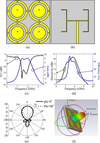
The FSS-based basic element of the planar antenna array for the proposed structure is demonstrated in Fig. 1(a). Initially, 2 × 2 array is designed as shown in Fig. 7(a).
Geometry of the four-element planar array, (a) front view, (b) bottom view and it simulated results, (c) S11 and gain, (d) directivity and efficiency, (e) 2-D radiation pattern, and (f) 3-D radiation pattern.

An additional F4B substrate is added below the ground to design a feeding network that incorporates T-junctions that excite individual elements as shown in Fig. 7(b). All circular patches are connected to the feeding network through metalized via of a diameter of 0.7 mm. The feeding network is connected to a single 50 Ω feed as shown in Fig. 7(b). The simulation of the planar antenna array is performed by CST MWS. In the simulation, all boundary conditions are set to be the open boundary. The simulated reflection coefficient (S11) realized gain, directivity, and efficiency of the basic four planar antenna array elements are given in Figs 7(c) and 7(d). It can be concluded from Fig. 7(c) that a good impedance matching bandwidth <− 10 dB, i.e. from 7.6 to 8.1 GHz has been achieved. From the realized gain, it is concluded that the basic four-element planar array exhibits a maximum peak of about 8 dB in the propagation direction. The 2-D and 3-D radiation patterns are given in Figs 7(e) and 7(f). The polar pattern for both phi = 0° and 90° is nearly the same and also the main lobe of the polar and 3-D radiation pattern points towards the normal direction.
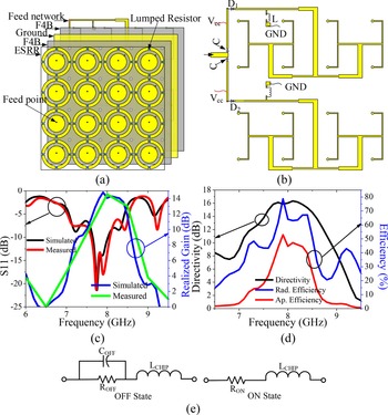
In order to design a high gain antenna, an array of 4 × 4 elements array is proposed and designed as shown in Figs 2(c) and 8(a). The total dimension of the surface is 2.1λ × 2.1λ at the resonance frequency of 7.8 GHz. In the circuit model of antenna and absorber, the switch S2 is required in the physical structure when the structure works as an antenna/radiator. Therefore, two p-i-n switches from SKYWORKS SMP1320 − 079 LF in the SC − 79 packages [49] are incorporated in the feeding network. The structure is regarded as an antenna/radiator when the p-i-n switches are switched ON, which means that the circular patches and feeding network areconnected to some input source signal as shown in Figs 1(a) and 1(d). The DC bias circuits of the p-i-n diodes are also illustrated in Fig. 8(b). As shown in Fig. 8(b), diode D1 and D2 are powered by the DC source (Vcc). The capacitor and inductor are embedded to isolate the RF and DC sections. The diodes D1 and D2 need to be operated with some DC source by applying Vcc where D1 and D2 are switched OFF when no source is applied.
The schematic view of the (a) multi-layered structure, (b) its feeding network, (c) return loss S11 and gain, (d) directivity and efficiency of the 4 × 4 elements array, and (e) states of diodes (D1 and D2). (Note: R OFF = 1 KΩ, C OFF = 0.35 pF, L CHIP = 1.5 nH, and R ON = 0.9 Ω, L = 50 nH, C = 100 pF and V cc = 3 V).

To evaluate the radiation performance, we measured and simulated S-parameter S11 and realized gain as presented in Fig. 8(c). It is shown that the S-parameter S11 is <− 10 dB and gain is increased linearly up to 14.5 dB over a frequency band from 7.5 to 8.0 GHz. The directivity of the antenna array is calculated as follow:

where A is the physical area of the antenna ground and k(0 ~ 1) is the effective coefficient. If k = 1, the theoretical value of the maximum directivity is given as:

Here the area of the aperture A = 82 × 82 mm2 and λo = 38.46 mm at f = 7.8 GHz. Using equation (5), the theoretical value of D dir. = 17.5 dB. Where simulated directivity D dir. = 16.12 dB as shown in Fig. 7(d). A little degredation between theoritical and simulated values may be due to lumped resistors in the outer ring or due to some other losses.
To maximize the performance of the antenna array, an optimal design of the array is carried out to maximize the array aperture efficiency. The aperture efficiency ɛ ap of the array can be written as:

where A em is the antenna array's effective maximum area and A physical is the physical area of the array aperture. The effective maximum area A em can be written as:

where λ is the wavelength at f = 7.8 GHz and G is the antenna gain. The aperture illumination efficiency is calculated at working frequency 7.8 GHz. Maximum aperture efficiency of $52.9\%$ is observed at 7.8 GHz as shown in Fig. 8(d). Where the radiation efficiency is defined as ɛ rad = G/D, where D is the directivity. The radiation efficiency is shown in Fig. 8(d), maximum radiation efficiency of $76\%$
 is observed at resonance frequency 7.8 GHz.
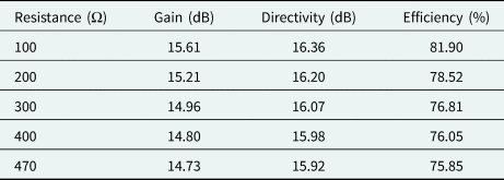
As the lumped resistors were fixed in the outer split-ring that has little impact on the radiation performance. In Table 1, simulated results are listed to demonstrate the impact of lumped resistors. As can be seen from Table 1, a little degradation is noted in gain, directivity, and efficiency when the value of lumped resistors is increased. Where in Refs. [Reference Li, Yi, Luo, Muneer and Zhu34, Reference Rahman, Cao, Gil, Sajjad and Wang35], the antenna elements exhibitlumped resistors, these lumped resistors have a great impact on the radiation performance. To reduce the effect of the lumped resistor, in this research, the disc-shaped radiating elements without lumped resistor are kept inside the absorbing circular element.
Impact of lumped resistors on gain, directivity, and radiation efficiency

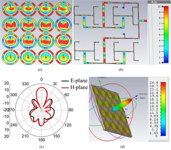
In Figs 9(a) and 9(b), the surface current is distributed uniformly over the circular-shaped patches and feeding network. The current is stronger in one direction of the circular-shaped patches and weaker in the other direction since each element was excited 1.2 mm away from the center of circular-shaped patches. Figure 9(b) shows that the current is equally distributed over the feeding network, where the high and low intensity of the current denotes the order of harmonics. To obtain identical radiation patterns, the disk-shaped patches were fed 1.2 mm away from the center but still at some angles the discrepancy between E- and H-plane radiation patterns is observed because the feed points impact both impedance matching as well as radiation pattern. However, the main lobe is directed along propagation while the (3 dB) angular width is about 23.50° as given in Figs 9(a) and 9(b).
The simulated surface current distribution: (a) top layer and (b) bottom layer. (c) The 2-D polar radiation pattern and (d) 3-D radiation pattern of 4 × 4 elements array.

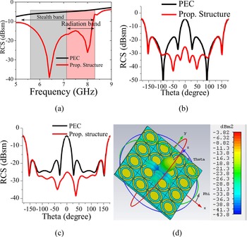
Since EM absorbers are primarily used to convert EM energy into other forms of energy such as heat or weaken them through interference cancellation that leads to RCS reduction. To evaluate the RCS reduction performance, we simulated the proposed structure as discussed in the above sections using a time-domain solver in CST. For the x-polarized incident EM wave, the mono-static RCS of the proposed structure is compared to the equal-sized copper sheet as displayed in Fig. 10(a). From Fig. 10(a) it can be seen that the RCS of the proposed structure drops over a frequency band from 6.2 to 8.2 GHz, which ensures that the proposed structure has low RCS in both stealth and radiating bands. The structure has a maximum RCS reduction of 39.18 dB within the stealth band at 6.2 GHz and 26.12 dB RCS reduction within radiating band at 7.8 GHz. The Cartesian bistatic scattering pattern at ϕ = 0° and ϕ = 90° is also depicted in Figs 10(b) and 10(c). It can be seen that the RCS is significantly reduced in a wide angular region. When ϕ = 0° the RCS reduces in the angular region 80° ≤ θ ≤ 80° while it remains same in − 80° ≤ θ ≤ −180° and 80° ≤ θ ≤ 80°, similarly when ϕ = 0° the RCS reduces in very wide angular region − 140° ≤ θ ≤ 140° while it remains same in the small angular region, i.e. in − 140° ≤ θ ≤ −180° and 140° ≤ θ ≤ 180°. The maximum reduction is observed around about 0°. Furthermore, the 3-D RCS scattering pattern is also shown in Fig. 10(d). It can be seen that mostly incident energy is deflected toward four directions.
The scattering characteristics of the designed surface: (a) mono-static RCS, (b) bistatic RCS (ϕ = 0°), (c) bistatic RCS (ϕ = 90°), and (d) 3 -D radiation scattering pattern at 7.8 GHz.

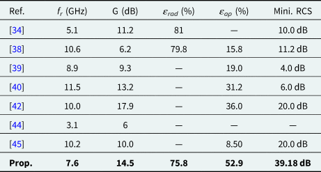
In Table 2, we have made a comparison of some significant performance parameters of the designed structure to those reported performance parameters in previously published research works. The designed MS structure in this research work exhibits high gain, low RCS, and high radiation efficiency. To be more persuasive and eradicate the factor introduced by the larger size of the designed surface, additionally we have calculated the aperture efficiencies. In this research work, the aperture efficiency is about $45\%$ , which is higher than other studies as listed in Table 2.
Performance comparison of the proposed structure with previously designed regular patch antennas

Note: f r, resonance frequency; G, gain; ɛ rad, radiation efficiency; ɛ ap, aperture efficiency.
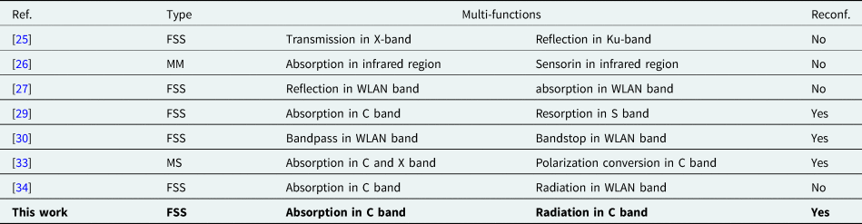
We further compare the novelty of this research work in Table 3. In Table 3, the previously designed structures have multiple functions to manipulate free space plane wave [Reference Sheng, Ge, Han and Zhu25–Reference Kiani, Weily and Esselle27, Reference Bakshi, Member and Mitra29, Reference Li, Cao, Liu and Wang30, Reference Li, Li, Wang, Wang and Cao33]. For example, in [Reference Sheng, Ge, Han and Zhu25], the designed structure has two alternate functions such as transmission in X-band and reflection in Ku-band. In this research study, two different switchable functions namely absorption and radiation are integrated. Compared with [Reference Li, Yi, Luo, Muneer and Zhu34], the proposed structure has a switchable function; however, the lumped resistors were embedded in radiating patch that degrades the radiation performance. The wideband absorption was achieved by embedding multiple resistors in multiple resonating rings with using the thick substrate.
Comparision with previously designed multifunctional EM structures

Note: Reconf., reconfigurability.
Conclusion
A multi-functional structure was designed for different functions namely absorption and radiation. The absorber is stable over an incident angle from 0° to 30°. The corporate feeding network which incorporates T-junctions is placed on the bottom layer. The p-i-n switches were embedded in the feeding network to alter the absorption and radiation functions. The structure behaves as a high gain and low RCS antenna with a maximum gain of 14.5 dB in the propagation direction. The low scattering characteristics of the proposed structure are also investigated. It is reasonable to believe the work can provide an alternative approach to constructing multi-functional structure with EM absorption and radiation functions and also to resolving the conflict among high gain and low RCS requirements.
Acknowledgement
The authors (S.U. Rahman, Q. Cao, Y. Wang) are gratefully acknowledge the financial support from the Natural Science Foundation of China under grant No. 61871219 and Jiangsu Postdoctoral Research Foundation under grant number 2021K308C
 Saeed Ur Rahman received a BS degree in electrical (electronics) engineering from the COMSATS University Islamabad, Pakistan in 2013 and a Master's degree in electronic engineering from the Capital University of Science and Technology (CUST) Islamabad, Pakistan in 2016. He received his Ph.D. degree in information and communication engineering from the Nanjing University of Aeronautics and Astronautics (NUAA), Nanjing, China in 2002. He is working as a postdoc research fellow at the College of electronics and information engineering, NUAA. His main research interests are the design of microstrip antenna, frequency-selective surfaces, metamaterial absorbers, polarization conversion, wearable antennas, and antenna arrays.
 Hai Deng received the Ph.D. degree in electrical engineering from the University of Texas at Austin, Austin, TX, USA, in 2000. He has been with the Department of Electrical and Computer Engineering, Florida International University, Miami, FL, USA, since 2009. He also taught electrical engineering at the University of New Orleans, New Orleans, LA, USA, and the University of North Texas, Denton, TX, USA. His research interests include radar systems, waveform design, signal processing, and radar networking systems.
 Qunsheng Cao is a professor of electrical engineering at Nanjing University of Aeronautics and Astronautics (NUAA) in China. Dr. Cao's current research interests are in computational electromagnetics, meta-material, frequency-selective surface, antenna design, and signal integrity for high-speed circuits. Dr. Cao has published more than 250 academic papers in refereed international journals and conference proceedings.
 Yi Wang received the B.S. and Ph.D. degrees in communication and information system from the Nanjing University of Aeronautics and Astronautics (NUAA), Nanjing, China, in 2006 and 2012, respectively. In 2012, he joined the College of Electronic and Information Engineering, NUAA, as an Assistant Professor, where he is currently working as an Associate Professor. His research interests include computational electromagnetics, especially the finite difference time-domain method, the FDTD.
 Muhammad Irshad Khan received the B.Sc. (Hons.) degree in electrical electronic engineering from the Comsats Institute of Information Technology Abbottabad, Pakistan and the M.Sc. degree in electrical engineering from the Capital University of Science and Technology, Islamabad, Pakistan in 2016. He is currently pursuing Ph.D. degree in electrical engineering from the University of Engineering and Technology, Peshawar, Pakistan. His research interests include microwave and RF circuit design, UWB antenna design and analysis, MIMO antennas, beam steering antennas, and reconfigurable antenna design.
 Zakir Khan received his B.Sc. engineering degree in telecommunication Engineering from the University of Engineering and Technology, Peshawar, Pakistan, in 2013 and the Master degree in electrical engineering from COMSATS Institute of Information and Technology, Abbotabad, Pakistan in 2016. He is currently pursuing the Ph.D. degree with the Department of Electronics science and Technology, University of Science and Technology of China. His research interests include microwave and millimeter wave antenna design, miniaturized antennas, wide band antennas, and multiband antennas.
 Muhammad Sajjad was born in 1990 and he received the BS degree in telecommunication from the University of Science and Technology, Bannu Pakistan, in 2013 and the MS degree in electrical engineering from COMSAT university, Pakistan in 2017. Recently he is pursuing his Ph.D. degree from Nanjing University of Aeronautics and Astronautics (NUAA), Nanjing, China. His research interests include electromagnetics and antennas especially metasurfaces, FSS, polarization conversation.
 Hisham Khalil was born in 1985. He received the BS degree in electrical engineering from the University of Lahore, Pakistan in 2008 and the Master's degree in electronic engineering in 2012. Thereafter, he received the Ph.D. degree in electrical engineering from Capital University of Science and Technology Islamabad, Pakistan. Currently, he working as an Assistant Professor since 2013. His research interests include analysis and design of printed antennas, conformal arrays, machine learning in microwave, and artificial intelligence.