I. INTRODUCTION
It is well known that intense electric pulses can significantly accelerate the dislocation movements, and thereby lead to a rapid recovery and recrystallization Reference Li, Shen and Xie1,Reference Conrad, Karam, Mannan and Sprecher2 or reduce the flow stress and increase the plasticity of metals undergoing plastic deformation (often referred to as electroplasticity). Reference Guan, Tang and Chu3–Reference Baranov, Staschenko, Sukhov, Troitskiy and Tyapkin8 Based on the electroplasticity, a variety of electropulse-assisted processing techniques have already been developed and demonstrated to be highly-effective and highly-efficient for various metallic materials such as aluminum, stainless steel [face-centered cubic (f.c.c)], Reference Tang, Zhang, Yan, Zhou and Fang5,Reference Nguyen-Tran, Oh, Hong, Han, Cao, Ahn and Chun9 low carbon steel [body-centered cubic (b.c.c)], Reference Nguyen-Tran, Oh, Hong, Han, Cao, Ahn and Chun9 magnesium, Reference Li, Wang, Li, Tang and Zhu7,Reference Xu, Tang, Tian, Ding and Tian10 and titanium [hexagonal close-packed (h.c.p)] Reference Song and Wang11,Reference Stolyarov12 and so on.
The acceleration effect on dislocation movement was first experimentally discovered by Troitskii and Likhtman in 1963 (Ref. Reference Troitskii and Likhtman13) and thereafter two categories of mechanisms were proposed in the subsequent decades. The first category of mechanism for the acceleration effect was based on the concept of direct interaction between drifting electrons and dislocations. Reference Troitskii and Likhtman13–Reference Stolyarov18 The basic idea is that, the drifting electrons can exert a stress (called “electron wind”) on dislocations and also enhance the mobility of dislocations on the usual slip planes (e.g., the octahedral planes for f.c.c metals) by reducing the activation energy for movement. The second group, although less popular, suggested that the accelerated dislocation movement was mainly caused by the current induced magnetic fields. Reference Molotskii and Fleurov19 It was proposed that the magnetic fields can change the core structure of dislocations and help in dislocation depinning from impenetrable obstacles. Reference Molotskii20,Reference Molotskii21
It is worth noting that the above theories, being microscopic in nature, have been quantitatively examined mainly by macroscopic mechanical experiments such as tensile tests, Reference Stolyarov18 creep, Reference Stashenko and Troitskii22 and stress relaxation, Reference Sprecher, Mannan and Conrad14 for which over simplification of the links between the micro- and macroscenarios are unavoidable. In other words, there are few direct microscopic experimental studies for the mechanisms of acceleration effect, which limit the confidence in the interpretation. The reason for the paucity of such research might be the difficulty of observing directly the movement of dislocation, especially the real time slip path under the action of electric pulse.
In this study, by applying a proper intensity of electric pulses on a prepared TEM sample at cryogenic temperatures, we succeeded to track the dislocation movements through an ex situ experiment and analysis of dislocation slip path indirectly from the slip traces. Interestingly, non-octahedral-like dislocation glides at cryogenic temperatures were evidenced in pure aluminum, revealing a new mechanism for the accelerated dislocation movement by electric pulses.
II. EXPERIMENTAL PROCEDURES
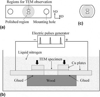
To dramatically reduce the ordinary Joule heating effect and highlight the nonthermal part, electric pulsing of a pure aluminum TEM sample in a liquid nitrogen bath (schematically shown in Fig. 1) was adopted for three benefits: (i) dislocation behavior might be tracked by TEM observation after the electric pulsing, since the sample can directly experience TEM observation without polishing; (ii) the electric resistance of aluminum is quite low and even more than an order of magnitude lower in liquid nitrogen (∼0.20 × 10⁻⁸ Ω m at 77 K) than at room temperatures (∼2.7 × 10⁻⁸ Ω m at 298 K), Reference Desai, James and Ho23 and thereby the Joule heating can be largely suppressed and the athermal effect of electric pulses might dominate; and (iii) the small volume and large surface/volume ratio of TEM samples ensure quick enough release of the ordinary Joule heating and therefore keeping of cryogenic temperatures in the samples. An additional method to reduce the ordinary Joule heating was to use a duty ratio of electric pulses as low as 1:32 to allow enough heat dissipation in the period of each pulse.
Schematic of electric pulsing experiment. (a) Rectangular TEM sample for electric pulsing. It was obtained from the longitudinal section of rolled aluminum sheet. RD is the rolling direction of rolled sheet, ND the normal direction. Microstructures before and after the electric pulse treatment in the dotted block regions were compared. (b) Electric pulsing of the rectangular TEM sample. The current direction is parallel to RD. The set up including the copper plates, wooden base, and applied pressures was designed to reduce the contact resistance and avoid possible damage of the thin sample during the electric pulsing. (c) Tailored TEM sample cut from the central part of the rectangular sample after the electric pulsing.

A. TEM sample preparation
The TEM samples were prepared as follows. Firstly, an aluminum ingot (99.7%, its chemical composition was summarized in Table I) with a thickness of 40 mm was cold rolled to 2.4 mm by 10 passes (the average thickness reduction was ∼25% per pass) and then a foil with a size of 11.5 (length) × 2.4 (width) × 0.5 (thickness) mm3 was cut from the longitudinal section of the rolled sheet, with the length parallel to the rolling direction (RD) and the width parallel to the normal direction (ND). Secondly, the foil was mechanically thinned down to 0.15 mm using abrasive papers and the central part of foil was then electrochemically polished by twin-jetting. The average cross-sectional area of the polished regions was about 0.25 mm2 determined by scanning electron microscopy (SEM) measurements. Finally, near the ends of foil mounting, holes were made for fixing the sample on a Gatan model 654 single-tilt holder (Pleasanton, California) for TEM observations [Fig. 1(a)].
Chemical composition of the aluminum ingot (99.7%).

B. Electric pulsing of TEM samples and temperature estimation
The electric pulsing of TEM sample was conducted in a liquid nitrogen bath (77 K) for 3 s [Fig. 1(b)], by using 58 Hz electric pulses with a small duty ratio of 1:32 (duration of each pulse: t p = 500 μs). Two electric current peak values (300 and 560 A) were adopted to explore its effect on the dislocation behavior and the corresponding microstructural changes. The temperature rise due to Joule heating was monitored by a ST50 type thermocouple (RKC, Tokyo, Japan) using a microprobe (diameter: 50 μm) with a short response time of 0.4 s, on 5 rectangular TEM samples prepared by the same manufacturing process and with the same electric pulsing parameters as those of the samples for post-TEM observations. The microprobe was glued to the polished regions of sample with two points carefully addressed to ensure reliable measurements of the temperature change in the sample: (i) there is no glue in the contact between the thermocouple and the sample, (ii) but there is enough glue between the probe and the liquid nitrogen bath for proper thermal insulation. During the whole electric pulsing, no electric sparks were observed around the polished holes of the TEM samples and the highest temperature rise among these samples was less than 5 K. Such result of measurement should be interpreted with caution, since the thermocouple cannot tell the highest temperature ever reached in the transient heating of a TEM sample (quite non-uniform in geometry) due to the finite reaction time (0.4 s) and spatial resolution (50 μm). All the temperature measurement (T < 82 K) from thermocouple can tell is that the Joule heat was efficiently dissipated and little was accumulated.
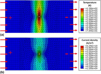
However, an upper-bound estimation of highest temperature in the sample can be made based on this information. The real highest temperature cannot exceed that in one pulse period in the adiabatic condition (the sample is thermally insulated from surroundings but internal heat conduction is allowed). The temperature rise, as well as the current density, of TEM samples at a peak current (e.g., 560 A) treatment was obtained by finite element method (FEM) simulation using the software Abaqus Reference Hibbit, Karlsson and Sorensen24 with the coupled thermal-electric elements (DC3D4E and DC3D8E), in which the real TEM sample geometry and material parameters for pure aluminum, especially the large temperature-dependent variation of electric resistance were considered. Reference Desai, James and Ho23 In the whole FEM simulation, the electric resistance of pure aluminum used here was chosen as the bulk average value neglecting the microscopic value of defects such as dislocations and grain boundaries. Figure 2 shows the spatial distributions of temperature and current density in the TEM sample. It can be seen that, the upper limit of temperature rise is less than 53 K, regardless of the ultrahigh transient current density ∼4 × 10¹⁰ A/m2. The small temperature rise indicated that the increase of electric resistance was limited and the low electric resistance remained. The electric resistance of aluminum at 130 K was ∼0.6 × 10⁻⁸ Ω m, still much lower than that (∼2.7 × 10⁻⁸ Ω m) at 298 K. Reference Desai, James and Ho23 The low electric resistance during the whole electric pulse treatment strongly suppressed the Joule heating.
Spatial distributions of temperature (a) and current density (b) of TEM sample after a single peak current (560 A) treatment in the adiabatic condition. The adiabatic condition is that, the sample is thermally insulated from surroundings but internal heat conduction is allowed.

It is worth noting that there were some differences between the measured and simulated temperature rise. The measured temperature rise was the result of the average Joule heating effect in the period of electric pulsing, while the simulated value was for the local peak temperature rise and calculated in the adiabatic condition, it's natural that the latter (∼53 K) is larger than the former (∼5 K). The measured temperature rise was less than 5 K, which could tell that little Joule heating was accumulated and the electric resistance of pure aluminum would not increase much. The simulated temperature rise at the peak current was less than 53 K, which could tell that the upper limit temperatures were below 130 K during the whole electric pulsing. These measurements and simulations together indicate that the highest temperature in the sample during the electric pulsing process was below 130 K in the observed regions.
C. Microstructure characterization
After the treatment, the TEM sample was tailored to a proper shape [Fig. 1(c)], in order that the microstructures can be systematically characterized by TEM using a double-tilt holder. The microstructures of the sample before and after the electric pulse treatment were characterized by a JEOL-2100 TEM (JEOL Ltd., Tokyo, Japan) operating at 200 kV. In this research, we mainly focused on electric pulses induced dislocation movements, which may be deduced from the changes of dislocation configuration or the analysis of slip traces. Therefore, the TEM microstructures were recorded under a multiple-beam condition
 $\left( {{\rm{B}}//\left[ {110} \right]} \right)$
, which can illuminate almost all interior dislocations (as well as slip traces). In some special cases, the nearby two-beam condition
 $\left( {{\rm{B}}//\left( {1\bar 11} \right)} \right)$
was also applied for a higher resolution of dislocations and slip traces.
III. EXPERIMENTAL RESULTS
A. As-rolled microstructures
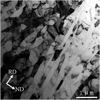
Figure 3 shows the typical lamellar structures of heavily rolled aluminum which was featured by extended lamellar boundaries almost parallel to the RD and short transverse boundaries interconnecting the lamellae. The sizes of lamellar grains are in submicron ranges (<1 μm), with an average lamellar boundary spacing of 350 nm and interconnecting boundary spacing of 850 nm.
TEM microstructures of heavily as-rolled aluminum.

B. Electric pulses induced dislocation movements revealed by ex situ TEM observations
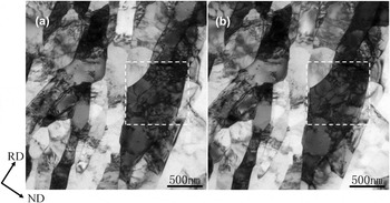
Figure 4 shows the overview of ex situ TEM observation of microstructural changes by the electric pulsing with a peak current of 300 A (current density in the observed regions: ∼2 × 10¹⁰ A/m2). No obvious changes were observed in the overall grain boundary contours and the intergranular contrasts. It indicates that the electric pulsing (with a peak current density of ∼2 × 10¹⁰ A/m2) could not cause significant grain boundary migrations at cryogenic temperatures.
TEM microstructures before (a) and after (b) the electric pulsing with a peak current of 300 A. To be noted, the two images were recorded under the same multi-beam condition (B//[110]) of the white dotted region. The enlarged images in the white dotted region are shown in Fig. 5.

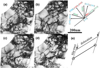
Nevertheless, there were some tiny changes of dislocation configuration in the white dotted block (Fig. 4). To highlight the changes, the microstructures of white dotted block in Fig. 4 were enlarged in Fig. 5. As illustrated by the arrows or circles (which show the intersections of a dislocation with upper and lower surfaces of foil) in Figs. 5(a)–5(d), a limited dislocation movement was tracked. Figure 5(e) shows the schematic of dislocation movement. It can be seen that, the trace of dislocation movement was parallel to the
 $\left( {01\bar 1} \right)$
or (101), which belongs to the non-octahedral planes in a face-centered cubic metal. It is worth noting that, during the whole ex situ TEM experiment, the influences of room temperature annealing and nitrogen bath clamping on the interior dislocation configurations could be ruled out, as indicated in Figs. 5(a)–5(c). Therefore, it can be concluded that the dislocation movement along the trace of non-octahedral {110} planes were solely caused by the athermal effect of electric pulses.
Analysis of dislocation movement by ex situ TEM observations. (a) As-rolled state. (b) Annealed at room temperature for one day. (c) Clamped in nitrogen bath for 120 s. (d) Electric pulsing (with a peak current of 300 A) for 3 s. (e) Schematic of dislocation movement. The inset shows the traces of stereographic projection for low-indice planes under the multibeam condition (B//[110]). The arrows in (a–c) indicate the intersections of a dislocation with the upper and lower surfaces of foil. No dislocation movements were induced by the room temperature annealing or nitrogen bath clamping. The dotted arrows and circles in (d, e) indicate the intersections before and after electric pulsing, respectively.

C. Electric pulses induced dislocation movements revealed by slip traces analysis
As the current reaches up to 560 A (current density in the observed regions: ∼4 × 10¹⁰ A/m2), the short period of electric pulsing induced tremendous microstructural changes (to be discussed in a separate paper), leaving plenty of slip traces, which can be used to identify the path of dislocation gliding through the crystal. Figure 6(a) shows an overview of the TEM microstructures recorded under the multiple-beam condition
 $\left( {{\rm{Beam}}//\left\langle {110} \right\rangle } \right)$
and Figs. 6(b)–6(f) show some enlarged images for slip traces analysis. The slip traces tell them from the image of dislocations in that, firstly, slip traces are straight lines (intersection of the slip plane with the foil plane) or connected straight segments (caused by cross-slips), while dislocations are often curved in aluminum (which has high stacking fault energy); secondly, slip traces exhibit weaker contrast than those of dislocations in the bright field image recorded under multibeam conditions.
Reference Caillard and Martin25–Reference Caillard and Martin27
Figure 6(b) (bright field image) shows a typical example where the slip traces and dislocations can be readily identified, and Fig. 6(c) (dark field image) shows a better resolution of the slip traces, which was recorded under the nearby two-beam condition
 $\left( {{\rm{Beam}}//\left( {1\bar 11} \right)} \right)$
.
TEM microstructures of the sheet after the electric pulsing with a peak current of 560 A. (a) An overview of TEM microstructures. The bright field TEM image was recorded under the multiple-beam condition
 $\left( {{\rm{Beam}}//\left\langle {110} \right\rangle } \right)$
that was able to illuminate almost all interior dislocations and slip traces. (b) Enlarged images of the dotted square blocks in (a). Under the multibeam conditions the boundary dislocations or the dangling dislocations are in a sharp dark contrast, whereas the contrast of slip traces is much weaker. (c) The corresponding dark field TEM image of (b). It was recorded under a two-beam condition
 $\left( {{\rm{Beam}}//\left( {1\bar 11} \right)} \right)$
nearby the multiple-beam condition
 $\left( {{\rm{Beam}}//\left\langle {110} \right\rangle } \right)$
. (d, e) Enlarged images of white dotted blocks in (c). (f) Enlarged images of the dotted rectangular blocks in (a). The inset shows the traces of stereographic projection for low-indice planes including octahedral planes {111} and non-octahedral planes {100} and {110}. Slip traces on the edge-on planes were highlighted in (d–f).

To be noted, under the view of the multiple-beam
 $\left( {{\rm{Beam}}//\left\langle {110} \right\rangle } \right)$
or the nearby two-beam
 $\left( {{\rm{Beam}}//\left( {1\bar 11} \right)} \right)$
condition, the low-indice planes, such as
 $\left( {\bar 111} \right)$
,
 $\left( {1\bar 11} \right)$
,
 $\left( {1\bar 10} \right)$
, and (001), were almost edge-on and the slip traces on these planes were featured by single lines rather than a couple of parallel lines.
Reference Caillard and Martin25–Reference Caillard and Martin27
Based on this feature and the stereographic projection of lattice planes in the inset of Fig. 6, the indices of slip traces on the edge-on planes can be unambiguously determined.
It can be clearly seen from Figs. 6(b) and 6(c) that, on a larger scale, the slip traces in most cases are parallel to the edge-on octahedral plane
 $\left( {1\bar 11} \right)$
, while on a finer scale as shown in Figs. 6(d) and 6(e), the slip traces may switch to the edge-on non-octahedral planes such as (001) and
 $\left( {\bar 110} \right)$
. Moreover, switches onto other higher-indice edge-on planes such as
 $\left( {1\bar 15} \right)$
,
 $\left( {\bar 221} \right)$
, and
 $\left( {3\bar 32} \right)$
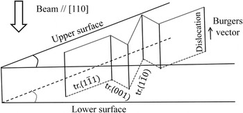
are observed in Fig. 6(f). As shown in Fig. 7, the switches of slip traces on the edge-on planes indicate the happening of cross-slips, and the Burgers vector of gliding screw dislocations can then be determined as 1/2 [110] (parallel to the view direction).
Schematic of cross-slips on the edge-on planes. The slip traces in the upper and lower surfaces were overlapping in the view of Beam//[110].

IV. DISCUSSION
As summarized from the above observations, a very short period of intense electric pulses (with a peak current density of ∼1010 A/m2) can cause the dislocation glides along the traces of non-octahedral planes in pure aluminum at cryogenic temperatures (<130 K).
However, due to the limited resolution the origins of slip traces observed for these non-octahedral planes cannot be unambiguously determined; they may originate from the following two possible dislocation glides
Reference Caillard and Martin28
: firstly, real dislocation glides on the non-octahedral planes and secondly intensive cross-slip between two octahedral planes [i.e.,
 $\left( {1\bar 11} \right)$
and
 $\left( {\bar 111} \right)$
] on a few atoms scale. We considered that the real dislocation glides on the low-indice octahedral {100} and {110} planes are more likely to occur than the intensive cross-slip between two {111} planes, since the {100} and {110} dislocation glides have been well confirmed in various high-temperature creep experiments.
Reference Caillard and Martin25–Reference Caillard and Martin27,Reference Carrard and Martin29,Reference Carrard and Martin30
Another evidence in favor of this assumption is pointed by the white arrow in Fig. 6(c), which suggests that the wavy slip trace parallel to
 $\left( {1\bar 11} \right)$
plane is caused by intensive switches among (001),
 $\left( {\bar 110} \right)$
, and
 $\left( {1\bar 11} \right)$
planes on quite a fine scale of tens of nanometers [Fig. 6(e)]. Additionally, the observed {110} planes dislocation slip in the Fig. 5 could be also positive in verifying the view of real dislocation glides.
Regardless of the origins, we may term the dislocation glides producing these slip traces in aluminum as “non-octahedral-like” dislocation glide. These non-octahedral-like dislocation glides can be viewed as a high-temperature-like behavior in that non-octahedral glides have only been observed at high temperatures (e.g., >453 K for aluminum) realized by high-temperature creep.
Reference Caillard and Martin25–Reference Caillard and Martin27,Reference Carrard and Martin29,Reference Carrard and Martin30
Although these non-octahedral slip traces bear much resemblance to those in high temperatures by ordinary heating, some differences do exist. Firstly, the slip traces on non-octahedral planes are much shorter here; secondly, the number of switches (cross-slips) among different slip planes over identical distance are much larger than that of previously observed switches at high temperatures; and thirdly the electric pulses can induce higher-indice non-octahedral-like dislocation glides [e.g., on
 $\left( {1\bar 15} \right)$
,
 $\left( {\bar 221} \right)$
, and
 $\left( {3\bar 32} \right)$
in Fig. 6(f)] than traditional heating (where on {100}, {110}, {112} and {113} were generally observed
Reference Caillard and Martin28
). The high-temperature-like dislocation glides in cryogenic temperatures as revealed by slip traces analysis indicate much improved freedom of dislocation behavior by applying electric pulses, and thereby the deformation resistance of a deforming metal can decrease significantly or the recovery process can be enhanced dramatically due to the new annihilation path. This actually offers a new scenario for accelerated dislocation movements in that new modes of dislocation glides are created by electric pulses, in comparison to previous theories appealing to increased dislocation mobility and/or extra force (“electron wind force”) for dislocation moving in usual slip systems (e.g., on {111} plane for f.c.c crystals).
Reference Sprecher, Mannan and Conrad14,Reference Molotskii and Fleurov19
In the current electric pulsing experiment the result of temperature measurements and simulations has indicated that the conventional thermal effect (in the global scale) of electric pulses was negligible, and thereby the athermal effect should account for microstructural changes (Figs. 5 and 6) as well as the high-temperature-like dislocation behavior. Generally, the athermal effects of electric pulses on crystals include magnetic field and pinch effect, Reference Molotskii and Fleurov19,Reference Okazaki, Kagawa and Conrad31 “electron wind force” on dislocations, Reference Boiko, Geguzin and Klinchuk15 thermal stress caused by rapid heating, Reference Zhang, Sui, Zhou and Li32 enhanced dislocation mobility Reference Sprecher, Mannan and Conrad14 etc. In the current electric pulsing experiment, the intrinsic magnetic field, as well as its related pinch effect, at the central part (observed regions) of TEM sample is negligible due to the offset of magnetic field from the two symmetrical sides. Reference Okazaki, Kagawa and Conrad31 The electron wind force calculated by σew = C ew J (where C ew is electron force coefficient [10−11–10−13 MPa/(A/m2) Reference Sprecher, Mannan and Conrad14 ] and J peak current density [∼1010 A/m2)] is in the range of 10−1 ∼ 10−3 MPa, much lower than the threshold stress (1–10 MPa) Reference Kamimura, Edagawa and Takeuchi33 to drive the dislocation slip in aluminum. Therefore, the electron wind force has little influence on the microstructural changes. Moreover, the thermal stress in not expected to activate the non-octahedral slip, since it has been demonstrated that high temperature is the uniqueness condition for non-octahedral dislocation glides in ordinary loading. Reference Carrard and Martin29,Reference Carrard and Martin30 Therefore, other uncovered athermal effects may dominate in this electric pulsing. Presumably, the local Joule heating, selective but not on global scale, might be the most probable cause for the appearance of high-temperature-like dislocation behaviors. The local temperature at the dislocation core could be much higher than in the surroundings when heated by high magnitude electric pulses because the electric resistance in the core (with the maximal lattice distortion) can be much larger than that in surrounding perfect crystal. Reference Caillard, Legros and Couret34,Reference Wert and Thomson35 Moreover, this concept of selective heating in dislocation core could also provide an explanation for the improved dislocation mobility, alternative to the concepts of electron wide force or magnetic effect. Reference Troitskii and Likhtman13–Reference Boiko, Geguzin and Klinchuk15,Reference Molotskii and Fleurov19–Reference Molotskii21 It should be pointed out that, the usual octahedral dislocation movements should be also accelerated by the electric pulse, because all the possible effects of electric pulses on the non-octahedral and octahedral slip should be the same or similar.
V. CONCLUSIONS
In summary, intense electric pulses can cause non-octahedral-like glides in aluminum at cryogenic temperatures. In spite of the overall low temperature measured in the samples, it can be recognized that the selective heating effect on dislocations might be the positive/deciding factor for the non-octahedral-like glides. Dislocations glide on non-octahedral-like planes can significantly increase the degrees of freedom for dislocation glides, and thereby offers a new/complementary explanation for the accelerated dislocation movements induced by electric pulses.
ACKNOWLEDGMENTS
The research was supported by the National Science Foundation of China (NSFC) under Project No. 51471107, 50971090 and by Center for Compression Science, Chinese Academy of Engineering Physics (Grant No. YK 2015–0602005), and by State Key Development Program for Basic Research of China (973 Programs) (Grant No. 2012CB619600).