Introduction
Modern high-frequency system equipped with multifunction transceiver subsystems is operating at multiple frequency bands. As an indispensible component of RF front end, the bandpass filter (BPF) enforces the overall performance of a system. Considering the present demand, the multiband BPFs have aroused a tremendous attention and numerous topologies have been proposed, such as multistub-loaded resonator in [Reference Wu, Jian, Chen and Su1, Reference Xu, Wu and Wei2] and multipath-embedded stepped impedance resonator in [Reference Wu, Chen and Chen3]. Most of the designs reported above have fixed operating bands and are unable to meet the stringent demand for adaptable frequency behavior. This leads into the realm of reconfigurable filter design where flexible operating frequency can be attained using a single filter. A farrago of methods has been adopted by the researchers to implement reconfigurable filters [Reference Hong4–Reference Ninic, Jokanovic and Meyer12] where PIN diodes are employed to tune the passband center frequency in discrete steps. Independently, switchable quad band BPF is reported in [Reference Weng, Hsu and Tu5] using PIN diodes, but its circuit size is large and additional stubs are required to improve passband selectivity. A reconfigurable BPF to switch between WiFi and UMTS reception standards for vehicular communication is presented in [Reference Brito-Brito, Llamas-Garro, Navarro-Muñoz, Perruisseau-Carrier and Pradell6], where six PIN diodes are utilized to achieve such switching characteristics at the cost of increased passband insertion loss. A dual-band BPF with single switchable band characteristic is achieved using PIN diode-loaded short stub resonator in [Reference Liu, Wei and Shi7]. The stepped impedance resonators [Reference Liu, Wei and Shi8, Reference Kim and Chang9] and microwave ring resonator [Reference Kim and Chang10] have been used effectively for the realization of reconfigurable BPF. A tri-state switchable filter is developed by employing a switchable slot in [Reference Mazloum, Jalali and Ojaroudi11]. The de-tuning technique among the split-ring resonators has been used in [Reference Ninic, Jokanovic and Meyer12] to switch from triple-band to several dual-band and single-band configurations, but the passbands suffer from poor selectivity.
In this paper, the passbands reconfiguration mechanism is presented. Initially, a tri-band BPF is implemented by assembling a pair of open-ended half wavelength uniform impedance resonator (UIR) and two pairs of quarter wavelength short-circuited UIRs. The novelty of the filter lies in its simple design structure, compactness, and capability of generating high selective tri-band response along with excellent stopband characteristics. Two PIN diodes are connected at the open edge of the short circuited resonators to bring the re-configurability on the two passbands. Depending on the bias voltage, the proposed filter can be switched from tri-band to two different configurations dual-band BPF and it can also be converted to a single-band BPF.
Design of triple-band bandpass filter
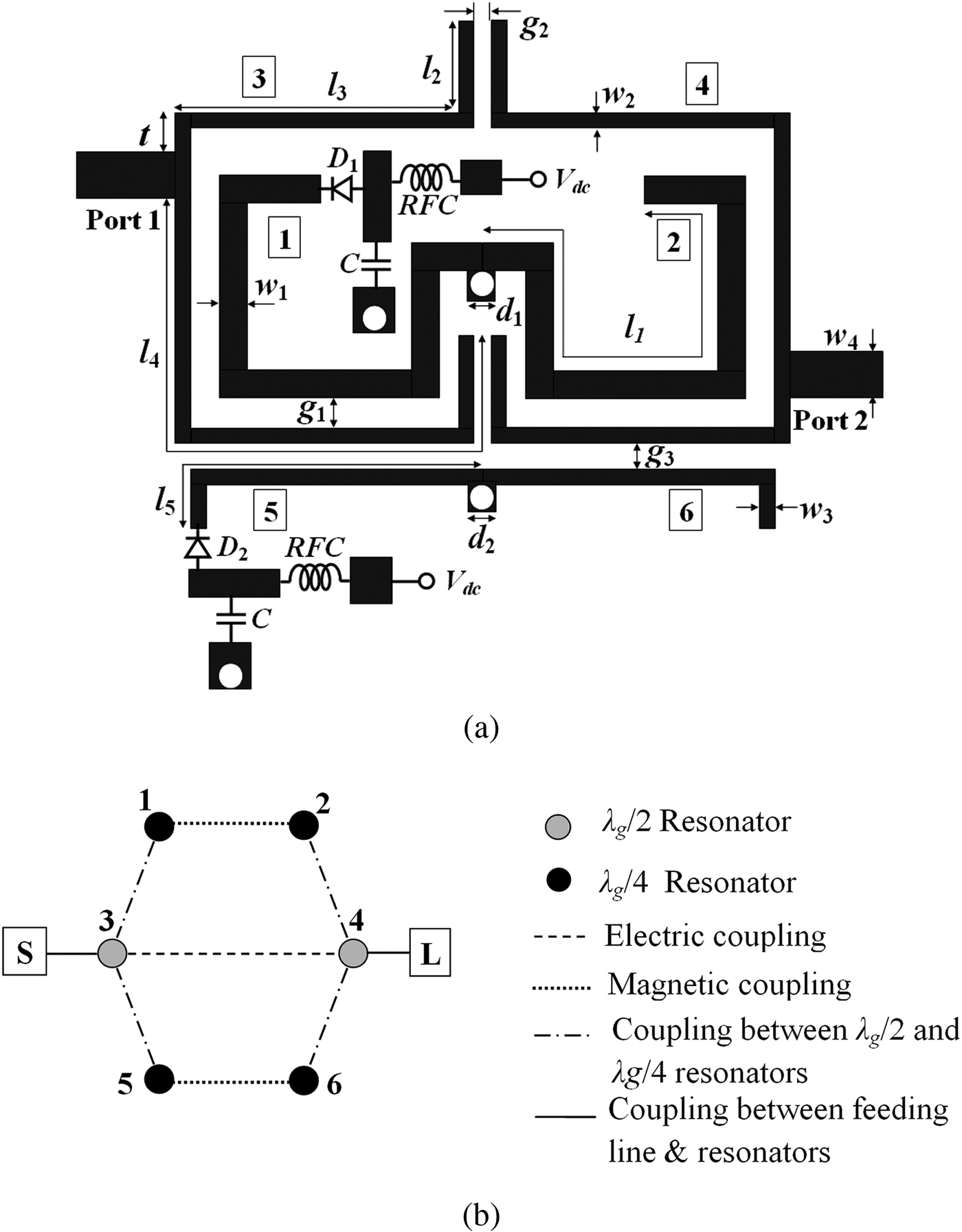
The layout of the proposed filter is illustrated in Fig. 1(a). It is realized on an FR-4 substrate with ε r = 4.4, tanδ = 0.002, and height (h) of 0.8 mm. The primary structure of the proposed filter works as a triple-band BPF. Two half wavelength open-loop resonators are utilized to achieve the passband resonance at 3.5 GHz. Two pairs of grounded quarter wavelength resonators are embedded near the open-loop resonators to implement the passband centered at 2.4 and 5.2 GHz. The fundamental resonance frequency of the resonators can be calculated as follows:
 $$f_{3.5} = \displaystyle{c \over {2(l_2 + l_3 + t + w_4 + l_4)\sqrt {\varepsilon _{eff}}}}, $$
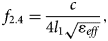 $$f_{2.4} = \displaystyle{c \over {4l_1\sqrt {\varepsilon _{eff}}}}, $$
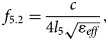 $$f_{5.2} = \displaystyle{c \over {4l_5\sqrt {\varepsilon _{eff}}}}, $$
where c is the velocity of light, ε eff is the effective dielectric constant.
Schematic depiction of the proposed filter. (a) Layout of the proposed filter with l 1 = 18.15, l 2 = 2.3, l 3 = 7, l 4 = 14.1, l 5 = 8.45, w 1 = 0.5, w 2 = 0.3, w 3 = 0.3, w 4 = 1.5, g 1 = 0.25, g 2 = 0.45, g 3 = 0.2, d 1 = 0.50, d 2 = 0.45, t = 0.9 (all dimensions are in mm). (b) The coupling scheme.

To comprehend the working mechanism, the coupling scheme of the proposed filter is shown in Fig. 1(b). The dark circles 1 and 2, 5 and 6 connected through dotted lines represent magnetic coupling between the grounded λ g/4 resonators. The gray-filled circles 3 and 4 connected through solid lines represent electric coupling between the λ g/2 open-loop resonators.
The filter design is initiated by selecting the lowpass prototype elements with values g 0 = 1, g 1 = 1.8219, g 2 = 0.6850, g 3 = 2.6599 for a second-order Chebyshev filter with 1 dB ripple factor. The fractional bandwidths (FBW) of three passbands are set as 7, 6, and 8% corresponding to 2.4, 3.5, and 5.2 GHz, respectively. Classical synthesis technique [Reference Hong and Lancaster13] is used to calculate the adjacent resonator coupling coefficient (M) and external quality factor (Q ex) of the tri-band filter.
Theoretically calculated coupling coefficients and external quality factors are M 12 = 0.062, M 34 = 0.053, M 56 = 0.071, Q ex2.4 = 26.02, Q ex3.5 = 30.36, Q ex5.2 = 22.77, respectively. The coupling coefficient M 34 helps in optimizing the coupling length and the gap between the resonators 3 and 4. On the other hand, M 12 and M 56 help in fixing the via diameters d 1 and d 2, respectively.
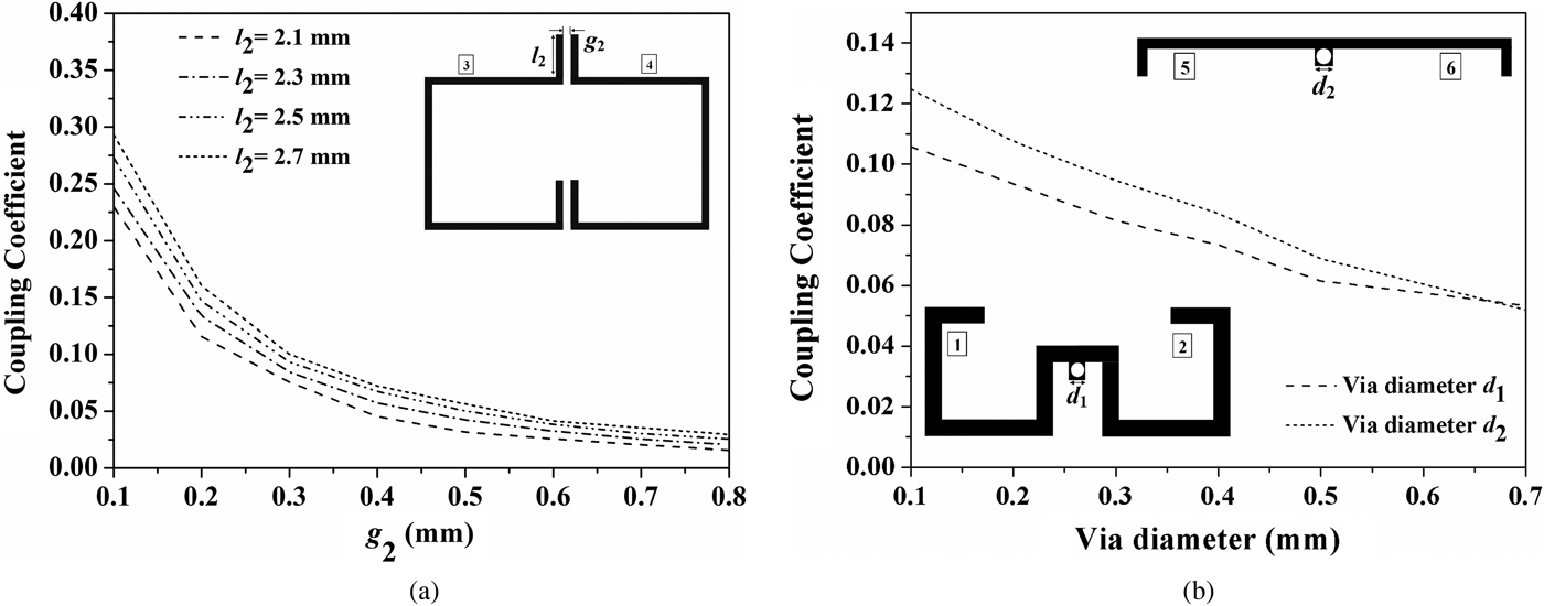
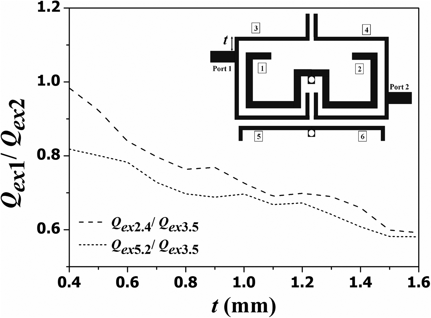
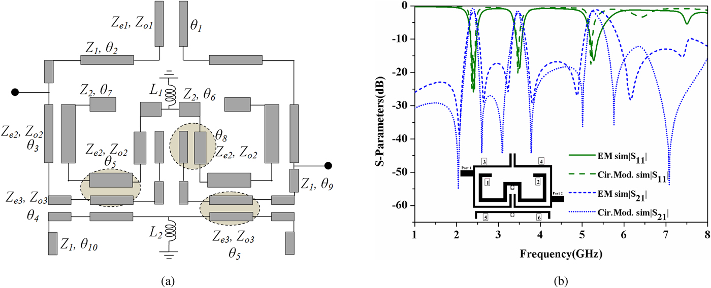
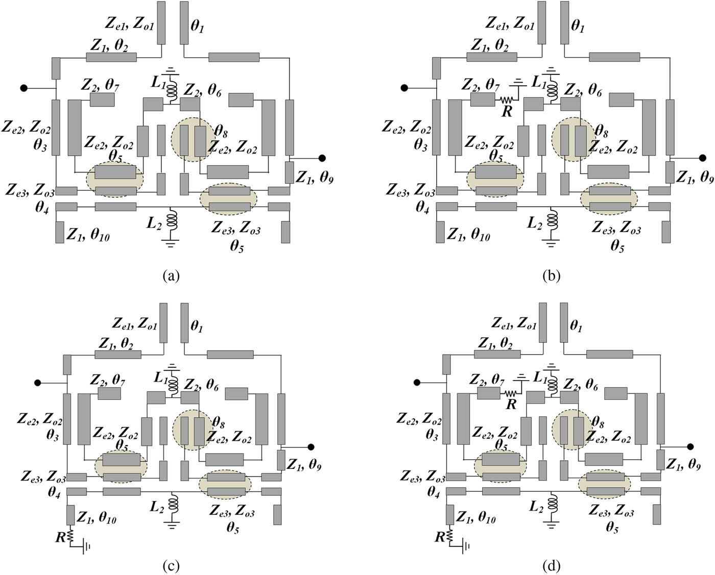
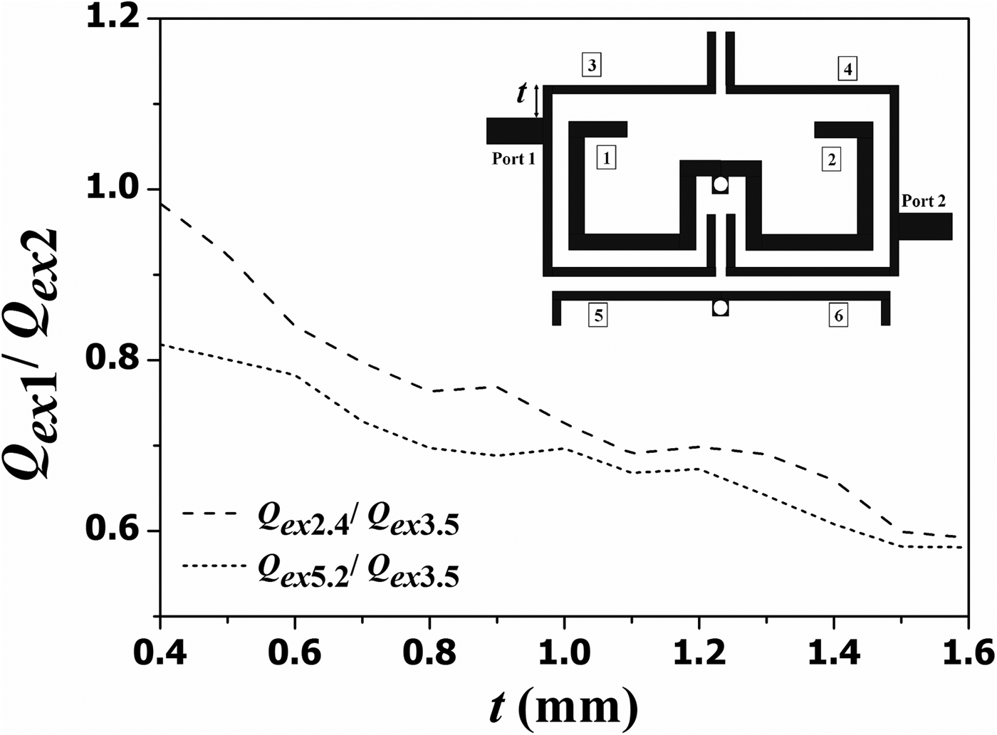
In order to determine the value of coupling gap g 2 and coupling length l 2 between the λ g/2 resonators, Fig. 2(a) is introduced. To achieve the desired coupling, the corresponding values of g 2 and l 2 are 0.45 and 2.3 mm, respectively. Figure 2(b) depicts the variation of the coupling coefficient for different via diameters. To ensure required coupling among the short circuited resonators, the values of d 1 and d 2 are found to be 0.5 and 0.45 mm, respectively. The resonators are placed adjacent to the open-ended λ g/2 resonator for the implementation of triple passband filter. The gaps g 1 and g 3 are optimized to meet the required coupling. To make the structure compact, the resonators are bended in different configurations. Finally, the tapping position (t) is determined as it is a crucial part of the filter design. The value of t directly depends on the value of the external quality factor (Q ex). Figure 3 unveils the normalized external quality factor for different tapping positions. The meticulous value of t can be predicted for the desired external coupling. The value is further tuned to 0.9 mm. To validate the theoretical analysis, EM simulation and transmission line model circuit simulation is carried out in ANSYS HF simulator. The transmission line model shown in Fig. 4(a) is designed using multisection symmetric and asymmetric coupled lines. A comparison of S parameters between EM simulation and equivalent transmission line model simulation is depicted in Fig. 4(b). Based on the simulated response, the electric lengths of different sections of transmission line model filter at 2.4 GHz are taken as θ 1 = 11.60°, θ 2 = 35.33°, θ 3 = 23.47°, θ 4 = 8.83°, θ 5 = 26.50°, θ 6 = 19.43°, θ 7 = 11.35°, θ 8 = 6.56°, θ 9 = 4.54°, and θ 10 = 4.54°. The even and odd impedance values of symmetric coupled lines are Z e1 = 135.26 Ω, Z e3 = 145.74 Ω, Z o1 = 79.36 Ω, Z o3 = 67.33 Ω, respectively. Whereas the even and odd impedance values of asymmetric coupled lines are Z e2 = 129.12 Ω, Z o2 = 62.15 Ω, respectively. The inductors L1 of 0.12 nH and L2 of 0.15 nH are used to provide magnetic coupling between adjacent resonators 1, 2 and 5, 6. Three distinct passbands are evidently visible at the center frequency of 2.4, 3.5, and 5.2 GHz. Six transmission zeroes are placed at either side of the passbands and it helps to improve the selectivity of the filter. Moreover, an upper stopband up to 8 GHz is achieved using the suggested filter topology.
Coupling coefficient of (a) λ g/2 resonator with different coupling lengths and gaps, (b) λ g/4 resonators with different via diameters.

The plot of the normalized external quality factor for different tapping positions.
(a) Transmission line model of the proposed filter. (b) Comparisons between EM-circuit simulated response of the filter without PIN diodes and biasing circuits.

Switchable filter design
In order to switch on/off the first and the third passbands, the PIN diodes are connected at the open end of the short circuited resonators to disperse the resonant frequency. The SMP1340-079LF pin diodes are placed at the open edge of resonators 1 and 5 with the DC biasing circuits. The bias voltage is applied through an RFC of inductance 27 nH, which is further connected to a 47 pF DC blocking capacitor. For the simulations, the PIN diode is modeled with a series resistor of 2 Ω in ON state and a series capacitor of 0.3 pF in OFF state. Transmission line models of different modes of operation depending on PIN diode state are shown in Fig. 5.
Transmission line equivalent circuit model of the proposed reconfigurable filter (a) when D 1 and D 2 are OFF, (b) when diode D 1 is ON and D 2 is OFF, (c) when diode D 2 is ON and D 1 is OFF, (d) when diodes D 1 and D 2 both are ON.

Results and discussion
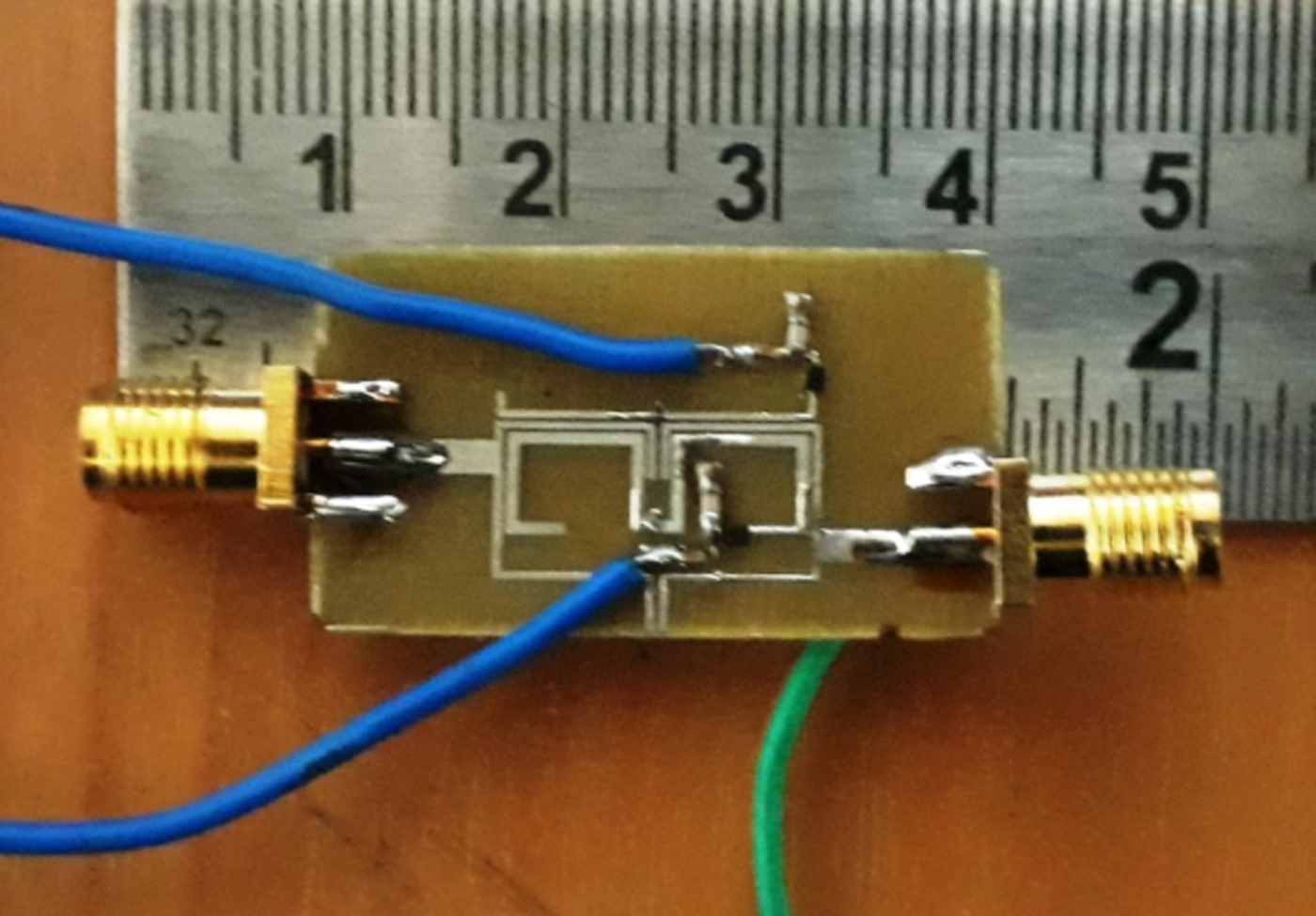
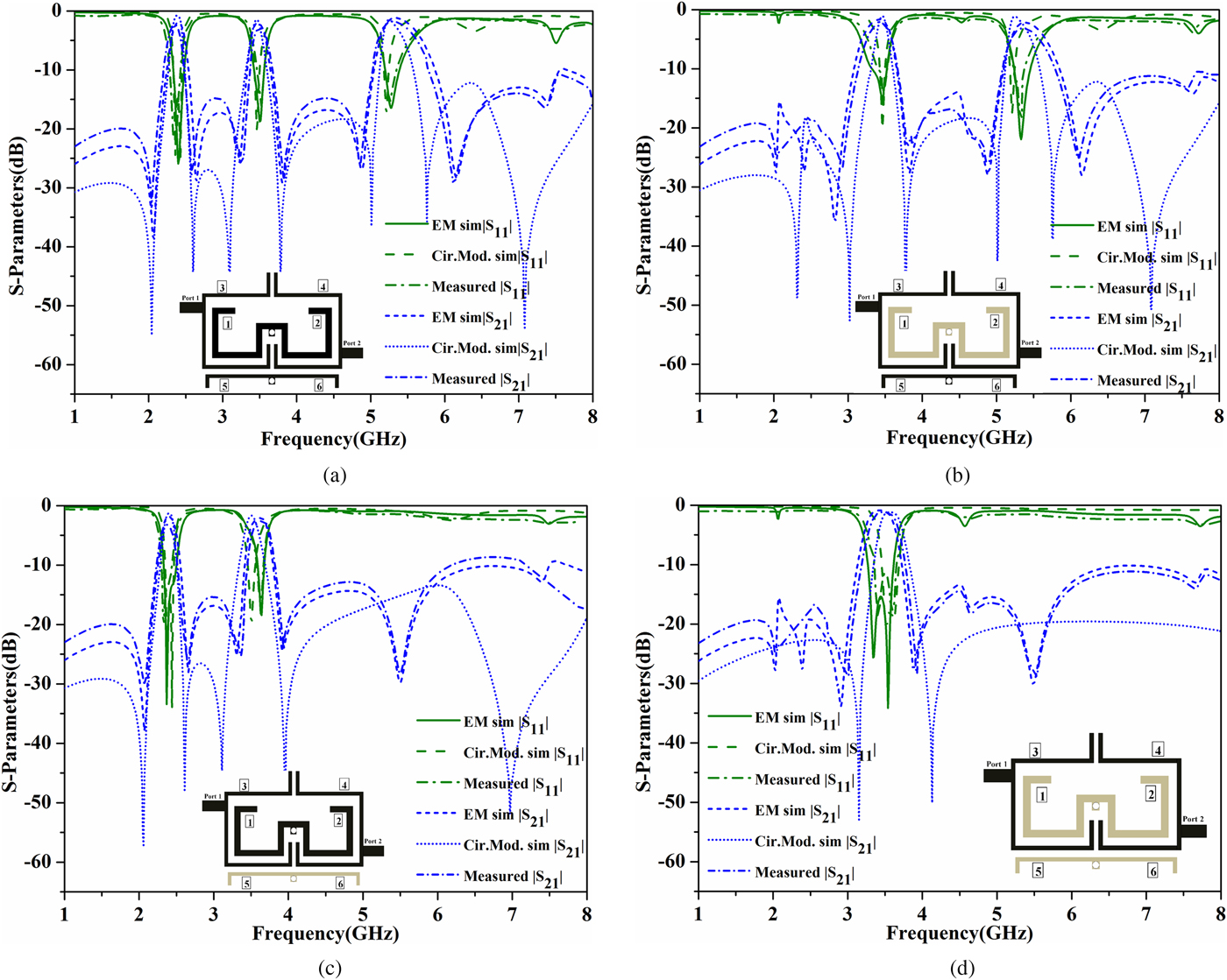
The fabricated prototype of the proposed switchable bandpass filter is shown in Fig. 6. The measurement of the filter is performed in R & S ZVA40 vector network analyzer. Comparisons of EM-simulated, circuit simulated, and experimental results are plotted in Fig. 7. It can be seen that the tri-bandpass response is preserved when all the diodes are switched OFF. The three passbands are measured at 2.42, 3.53, and 5.18 GHz with 3 dB FBW of 7.9, 6, and 9.1%, respectively. Six transmission zeros measured around each passband are located at 2.07, 2.61, 3.2, 3.81, 4.88, and 6.22 GHz, respectively. The resonators 3 and 4 have a 0° feed structure which helps in generating transmission zeros on each side of 3.5 GHz band. The resonators 3 and 4 act as a source and load coupling line for the resonators 1 and 2, 5 and 6. Due to multipath coupling, transmission zeros are created on each side of 2.4 and 5.2 GHz bands.
Fabricated prototype of the proposed filter.

Comparisons of EM-simulated, circuit-simulated and measured response of the proposed filter (a) when diodes D 1 and D 2 are OFF, (b) when diode D 1 is ON and D 2 is OFF, (c) when diode D 2 is ON and D 1 is OFF, (d) when diodes D 1 and D 2 both are ON.

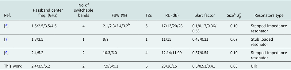
To accomplish the switching operation, V dc of 3.3 V with a forward current of 3 mA is applied to make the pin diode on. The first passband can be turned off by switching on the diode D 1. Due to forward bias, the guided wavelength of the resonator1 changes from λ g/4 to λ g/2. The asymmetric resonating length between resonators 1 and 2 stops the signal propagation at 2.4 GHz. As a result, the passband collapses with an insertion loss of 22 dB. The passband performance centered at 3.5 and 5.2 GHz is conserved. When the diode D 1 is OFF and D 2 is ON, the 5.2 GHz band is switched off with an insertion loss of 15 dB. So the filter provides dual-band response centered at 2.4 and 3.5 GHz. Finally, when both the diodes are switched ON, the proposed filter behaves like a single passband filter with a center frequency of resonance 3.5 GHz. The collapsed passbands are attenuated with an insertion loss of 15 dB. The measured insertion losses in every passband are <1.9 dB. The proposed filter also shows excellent upper stopband characteristics which are extended up to 8.0 GHz. A comparison with the proposed work and other published works is illustrated in Table 1. Compared to the other reported topology, the proposed reconfigurable filter has excellent selectivity due to the presence of transmission zeroes at either side of the pass bands. The skirt factor is introduced to measure the selectivity of the filter. It can be observed that the value of skirt factor is excellent in every passband. The return loss characteristics of each passband are satisfactory and the size of the filter is very compact compared to the other reported works.
Performance comparison with some switchable BPFs
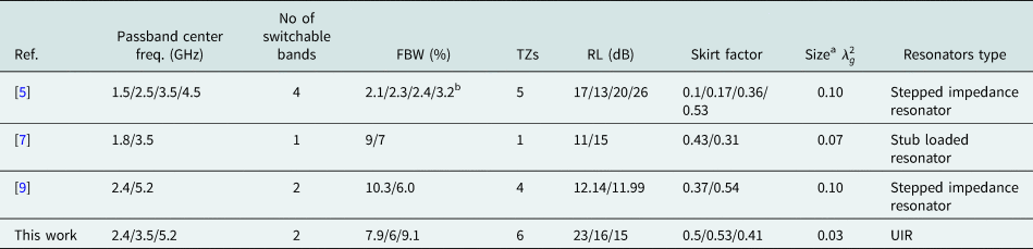
a λ g corresponds to the guide wavelength of the lowest frequency band.
b Theoretical values.
TZs, transmission zeros; RL, return loss; skirt factor: ratio between 3 dB and 20 dB bandwidths of the passband.
Conclusion
A novel compact reconfigurable BPF is reported in this paper. The switchable triple-band BPF is configured using two PIN diodes. Depending on the bias voltage, the triple passband characteristics can be tuned to two different configurations of dual bands as well as a single passband BPF. The resonators arrangement and the feeding structure reflect excellent passband selectivity. The upper stopband characteristic improves the performance of the filter. The size of the proposed filter is extremely small being about 0.20 λ g × 0.15 λ g at 2.4 GHz.
 Anjan Bandyopadhyay received the M.Tech. degree (Microwave Engineering) from The University of Burdwan in 2014. Presently, he is pursuing Ph.D. from the National Institute of Technology Durgapur. His research interest lies in the design of planar bandpass filters.
 Pankaj Sarkar received his M.Tech. degree from Burdwan University and Ph.D. from Jadavpur University in the years 2009 and 2016, respectively. He worked 1 year in the Space Applications Center – Ahmedabad as a trainee for the M.Tech. project entitled as “Design of MMIC Mixer at 50–60 GHz”. He initiated his teaching carrier from ITER (Siksha “O” Anusandhan University – Bhubaneswar), after that he served at the Sikkim Manipal Institute of Technology and the National Institute of Technology – Sikkim. Presently he is an Assistant Professor in Electronics and Communication Engineering Department of the North-Eastern Hill University – Shillong. He has more than 35 publications in various national/international journals and conferences. He is the reviewer of various journals such as IEEE Microwave and Wireless Components Letters, Electronics Letters, IET Microwaves, Antennas and Propagation, Progress in Electromagnetics Research (PIER), etc. His research interest lies in the area of microwave passive circuit design, metamaterials, MMIC, antenna.
 Tapas Mondal received the B.E. degree in Electronics and Telecommunication Engineering from Dr. B. A. M. University, Aurangabad (Maharashtra), M.E. degree in Microwave Engineering from Birla Institute of Technology, Mesra (BIT Mesra), Ranchi, and Ph.D. in Engineering from Indian Institute of Engineering Science and Technology, Shibpur (IIEST Shibpur), West Bengal, India in the years 2001, 2003, and 2018, respectively. He is currently an Associate Professor in Electronics and Communication Engineering Department at Dr. B. C. Roy Engineering College, Durgapur, India. His research interests include planar antenna, microwave devices, wireless communication and intelligent transport systems applications. He is a member of IEEE and life member of ISTE. He is a reviewer of IEEE, IET, Elsevier, John Wiley and PIER journals. He has organized the IEEE Workshop on Microwave Engineering and Applications in 2015.
 Rowdra Ghatak received his M.Tech. degree (Microwave Engineering) from The University of Burdwan and Ph.D. (Engineering) from Jadavpur University. He initiated his career in microwave engineering as a trainee at CEERI Pilani in fabrication and testing of S-band magnetrons. There after he served at the National Institute of Science and Technology Berhampur, Odisha and at the University of Burdwan. He is presently a Professor in Electronics and Communication Engineering Department of the National Institute of Technology Durgapur. He is a recipient of the URSI Young Scientist Award in 2005. He received support under DST Young Scientist scheme for the development of UWB antennas for imaging RADAR. He has more than 250 publications in various national/international journals and conferences. His research interest lies in the areas of fractal antenna, metamaterials, application of evolutionary algorithms to electromagnetic optimization problems, RFID, computational electromagnetic, and microwave passive circuit design. He is a reviewer of IEEE, IET, Elsevier, John Wiley and PIER journals. He has organized workshops in the capacity of workshop chair/convener on microwave circuits and antenna and has been a member of technical program committee membership of numerous IEEE conferences in the Asia Pacific region. He was a student paper contest co-Chair in the IEEE AEMC 2013 and Technical program co-chair at IEEE MicroCom 2016 and conducted numerous technical lectures.