
Introduction
Polydimethylsiloxane (PDMS) is currently one of the most useful materials for fabricating microfluidic channels and for manufacturing biomedical devices.[Reference Odom, Love, Wolfe, Paul and Whitesides1–Reference Dahiya, Gottardi and Laidani4] To extend the potential applications of PDMS, a wide range of semiconductor processes, including photolithography, electron beam lithography, and nanoimprint lithography, have been adopted. Polymerized siloxane (Si–O–Si), the backbone of silicone elastomer, offers mechanically flexible and visibly transparent structures that are well suited for imaging biomolecules, including DNA, proteins, and particles.[Reference Huh, Mills, Zhu, Burns, Thouless and Takayama5–Reference Pedron, Polishetty, Pritchard, Mahadik, Sarkaria and Harley8] Unlike polystyrene (PS), quartz, and glass materials, PDMS can be easily fabricated by simply mixing and curing the reagents of silicone elastomers using benchtop tools equipped in existing biomedical laboratories. In this respect, one of the essential elements to scale up the PDMS fabrication is to prepare recyclable silicon (Si)-wafer mold structure.
There are some problems in the recycling process of Si mold when repeating PDMS fabrications. One among them is the interaction between the siloxane compound of the cured PDMS and the Si mold, which leaves residues in the peeling-off process. The residue problems are often due to local chemical bonding or mechanical stretching of the siloxane compound to Si when PDMS is separated from the Si substrate. In particular, this behavior is most likely to occur at the finest features, which jeopardizes the repeated usage of the Si mold. This critically hinders the large-scale mass production of PDMS chambers. Thus, an optimal process is needed to overcome this problem.
Here, we offer a fabrication method of PDMS chambers which can be coupled with high-resolution fluorescence imaging system to real-time visualize single DNA molecules. There are two challenges addressed here. One is to extend the PDMS fabrication to 200 mm Si-wafer scale, ideally in pursuit of mass productions. To accomplish it, we introduce Si “mesa”-type structures with “nanoscallop” sidewalls to facilitate the PDMS residue-free peel-off process.[Reference Kang, Lee, Jung, Jung, Hwang and Ko9, Reference Chen, Ayon, Zhang and Spearing10] The idea of the sidewall-modifying process has been proved in the fabrication of nanoscale features of PDMS.[Reference Kim, Zarzar, He, Grinthal and Aizenberg11] We extend it to implement 200 mm wafer-scale productions of PDMS chambers. The second one is to optimize a high-resolution imaging system with the fabricated PDMS microfluidic chambers. Owing to the millimeter thick ceiling of PDMS chambers, it is often regarded as being difficult to couple the PDMS microfluidic devices with either a high-resolution oil-immersion optic system or a high-resolving power lens, since these lenses normally have short free-working-distance (FWD) as shallow as 100–200 µm (which is rarely suitable for ~150-μm-thick cover glass). To overcome this issue, we used a confocal microscopy with an objective lens having a proper FWD such as ~2.0 mm. To some extent, the purpose of this strategy is to keep a balance of obtaining a high image resolution against the ample working space, enabling us to introduce PDMS fluidic chamber for single molecule imaging. By assembling the fabricated PDMS chamber with the high-resolution optic system, we offer a protocol to real-time visualize the fluorescence images of single DNA molecules flowing inside the fabricated PDMS microfluidic chamber.
Experimental
The 200 mm diameter Si wafers were used to prepare mold structures for PDMS chamber fabrications. Positive-type photoresist (PR, AZ GXR601, ~1 µm thickness) was spin-coated upon the bare Si wafer, and exposed by ultraviolet (UV) via photomask aligner (Karl Suss MA8). The UV-exposed PR was developed in TMAH 2.38% solution for 1 min. The PR patterns were transferred to the Si substrate by deep reactive ion etching (DRIE, Alcatel AMS 200, Bosch process). A repeated etching step by C4F8 and SF6 gas plasma was performed to generate the nanoscallop geometry at the sidewall of “mesa”-type Si patterns. To create the scallop geometry, C4F8 plasma makes the surface of Si passivated by fluorocarbon-based polymer while SF6 plasma induces ion-bombardments preferentially on the bottom of the Si surface to lead vertical etching.[Reference Kang, Lee, Jung, Jung, Hwang and Ko9, Reference Chen, Ayon, Zhang and Spearing10] Under 2000 W RF power with 70 W back-bias condition, Si wafer was etched with the etch rate of 1 µm/min for 2 min. After the DRIE process, the remained PR was stripped by O2 plasma.
For PDMS chamber fabrication, the reagents of Sylgard 184 Silicone elastomer kit (Dow Corning) were mixed with a base-to-curing agent ratio of 10:1. The mixed PDMS reagent solution was poured on the 200 mm Si mold and degassed in a vacuum desiccator for ~2 h. The PDMS was cured at 90 °C on a hot plate for 1 h. After curing, the PDMS upon the Si-wafer mold was shaped by cutter and peeled off from the Si mold. The PDMS was punched with 1 mm holes for tube connections. After the surface of the PDMS was activated by tesla coil in an air condition at room temperature, the PDMS chamber was assembled with 1.2-mm-thick slide glass (76 mm × 52 mm area size). The assembled PDMS–slide glass was baked on the hot plate at 90 °C for ~2 h.
To test fluorescence imaging, PS particles with red dye (Spherotech, Fluorescent PS, 0.4–0.6 µm, Nile Red) was used. The size of the PS particle is 500 nm approximately.
To prepare DNA molecules, lambda (λ)-DNA (New England Biolabs, 500 µg/mL in 10 mM Tris–HCl, pH 8.0, 1 mM EDTA) was diluted in TE buffer solution with 50 pg/μL concentration. In the solution, 2-mercaptoethanol (Aldrich) and Tween 20 (Sigma) were added with 3% and 0.1%, respectively. The λ-DNA was stained with YOYO-1 iodide (Thermo Fisher, 1 mM in dimethyl sulfoxide) at the concentration of five base pairs per one dye molecule. The solution was incubated at room temperature for 5 h and stored at 4 °C refrigerator.[Reference Huh, Mills, Zhu, Burns, Thouless and Takayama5–Reference Jo, Dhingra, Odijk, de Pablo, Graham, Runnheim, Forrest and Schwartz7, Reference Wang, Nam, Cotte, Jahnes, Colgan, Bruce, Brink, Lofaro, Patel, Gignac, Joseph, Rao, Stolovitzky, Polonsky and Lin12–Reference Kundukad, Yan and Doyle14]
For fluorescence imaging, the assembled PDMS–slide glass sample were mounted on a confocal laser scanning microscope (Carl Zeiss LSM 700, inverted microscope). The illumination laser has 488 nm wavelength and 100 mW power. An objective lens has 20 × magnification with numerical aperture of 0.50 [Objective EC Plan-Neofluar 20 × /0.50 M27, free working distance (FWD) = 2.0 mm]. To record the movie, the laser scanning speed was 0.625–2.5 s per frame. Photomultiplier tubes (PMT) capture the microscopy images, both fluorescence image and differential interference contrast (DIC) image.
Results and discussion
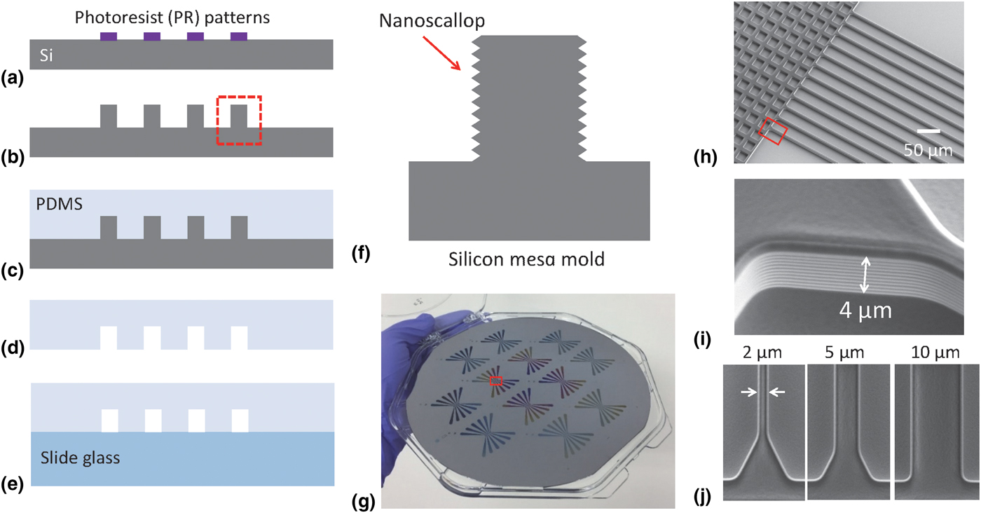
As an initial step to build PDMS microfluidic chambers, we prepared Si mold structure by conventional photolithography followed by DRIE. Figures 1(a)–1(e) show a schematic of the process-flow of 200 mm wafer-scale productions of the Si molds followed by the fabrication of PDMS chambers. As shown in Fig. 1(a), the patterns are generated on PR upon 200 mm bare Si wafer. The PR patterns are transferred to the Si substrate by DRIE, as shown in Fig. 1(b). The DRIE process consists of the alternating CF4 and SF6 plasma processes that correspond to passivating and etching cycles, respectively. This allows for a formation of nanoscallop geometry on the sidewall of the “mesa”-type Si patterns. A mixture of PDMS and its agent is poured upon the Si mold in Fig. 1(c). After the PDMS is cured, it is peeled off from the Si mold as shown in Fig. 1(d). The PDMS is punched with holes for afterward tube connections. After the bottom surface of the PDMS is activated by plasma, it is assembled with the slide glass, as shown in Fig. 1(e), which serves as a microfluidic device.
Fabrication of silicon (Si) mold and polydimethylsiloxane (PDMS) chamber. (a) Patterns are generated on photoresist (PR) by the photo-aligner process. (b) The PR patterns are transferred to the Si substrate. (c) PDMS mixture solution is poured upon the Si substrate. (d) After curing process, the PDMS is peeled off. (e) The PDMS is assembled with slide glass. (f) The sidewall of the Si mold has a nanoscallop geometry aiding a residue-free peel-off process of PDMS. (g) Camera image of 200 mm Si-wafer mold structure. (h) 30o-tilted view of SEM image of the red-rectangular area in (g). At the center of the device, Si mesa-type mold structures for microchannels are located. (i) 30o-tilted view of SEM image of the red-rectangular area in (h). At the sidewall of the mesa-type Si patterns, a finely tuned nanoscallop profile is identified. (j) Top-down view of SEM image of critical dimension (CD) features such as 2, 5, and 10 µm.
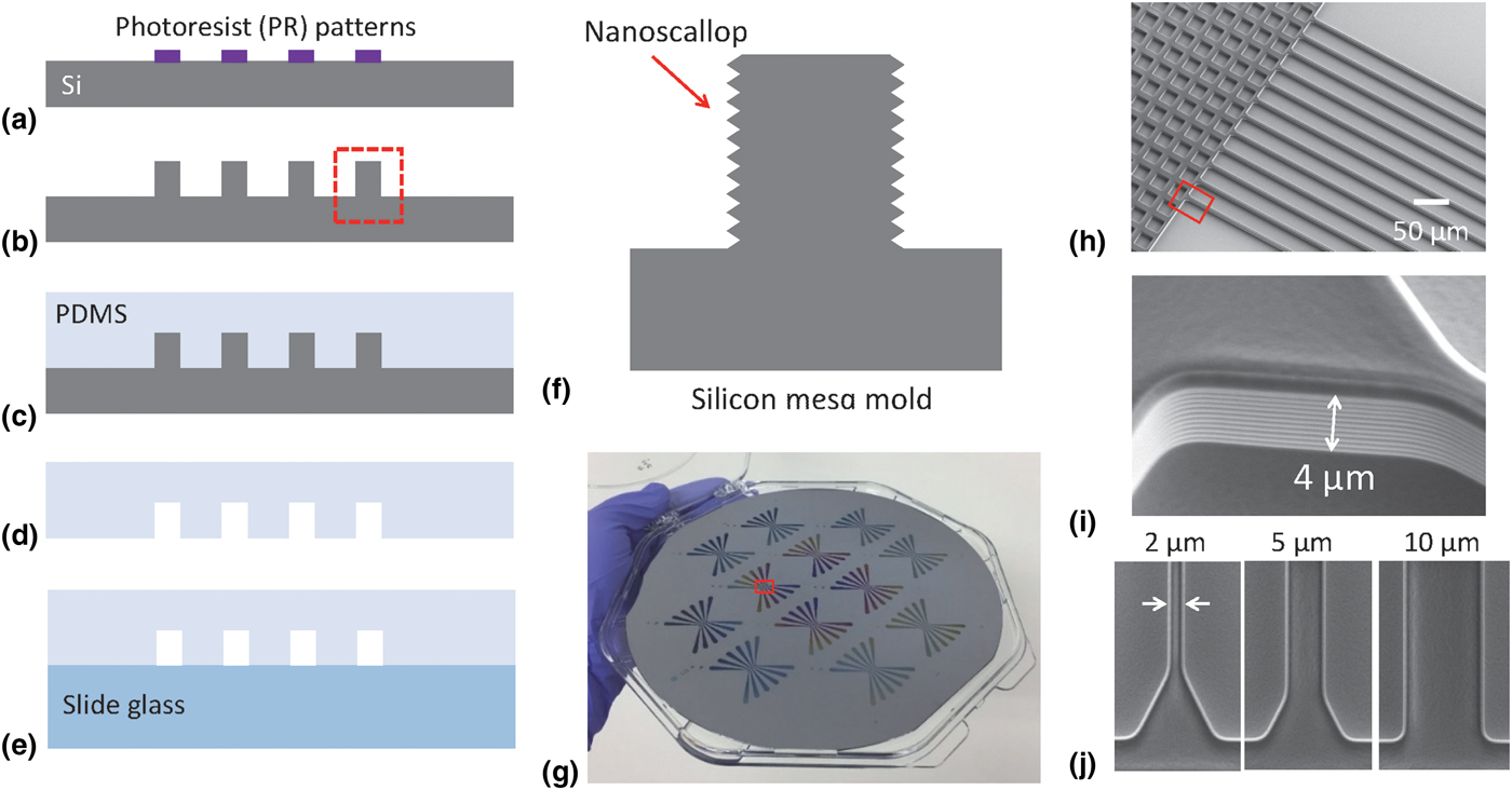
Figure 1(f) illustrates a magnified picture of the red rectangle area in Fig. 1(b), which shows a nanoscallop geometry created on the sidewall of the patterned Si “mesa”. The nanoscallop geometry is identified by cross-sectional scanning electron microscope (SEM) image as shown in Supplementary Figure S1, which displays a periodically modulated surface along the sidewall. Our strategy is to utilize the nanoscallop geometry as a key feature to facilitate a rapid and residue-free removal of the PDMS from the Si mold. Researchers have used SU-8 epoxy material as a mold for PDMS fabrications.[Reference Jo, Lerberghe, Motsegood and Beebe2, Reference Jo, Dhingra, Odijk, de Pablo, Graham, Runnheim, Forrest and Schwartz7] However, SU-8 epoxy has a limitation in demonstrating the pattern size < ~10 µm, and the pattern height which is only controlled by the spin-coating process. On the other hand, the Si patterns are ideally possible even for sub-20 nm features, and the pattern depth is well controlled by the RIE process, thus a fine-tuning of both lateral and vertical dimensions is viable with high scalability over the 200 mm large area.[Reference Wang, Nam, Cotte, Jahnes, Colgan, Bruce, Brink, Lofaro, Patel, Gignac, Joseph, Rao, Stolovitzky, Polonsky and Lin12]
Figure 1(g) shows a camera picture of 200 mm Si-wafer mold structure. The red rectangle area in Fig. 1(g) is magnified as shown in the SEM image of Fig. 1(h) which shows the “mesa”-type Si mold structure. Another red rectangle area in Fig. 1(h) is magnified as shown in Fig. 1(i). The 30o tilted-view SEM image of Fig. 1(i) shows the sidewall profile of the Si mesa by displaying a finely tuned nanoscallop geometry. The periodicity of the modulation in the nanoscallop is measured as ~400 nm which is confirmed by cross-sectional SEM image in Supplementary Fig. S1. The top-down SEM image in Fig. 1(j) shows the Si mold with different lateral dimensions, such as 2, 5, and 10 µm. We note that our fabrication method has a controllability over the channel size of the sub-10 µm dimension.
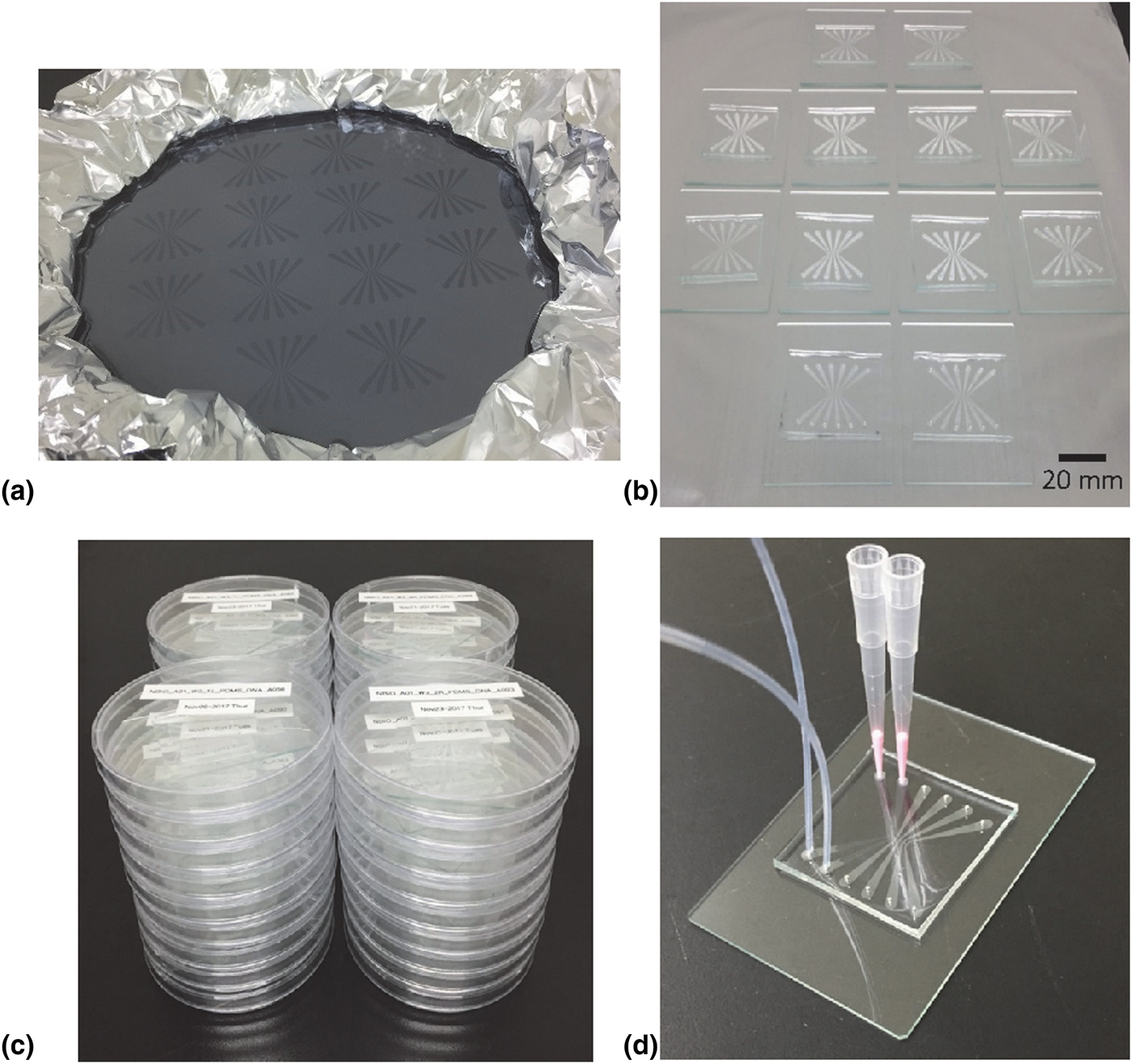
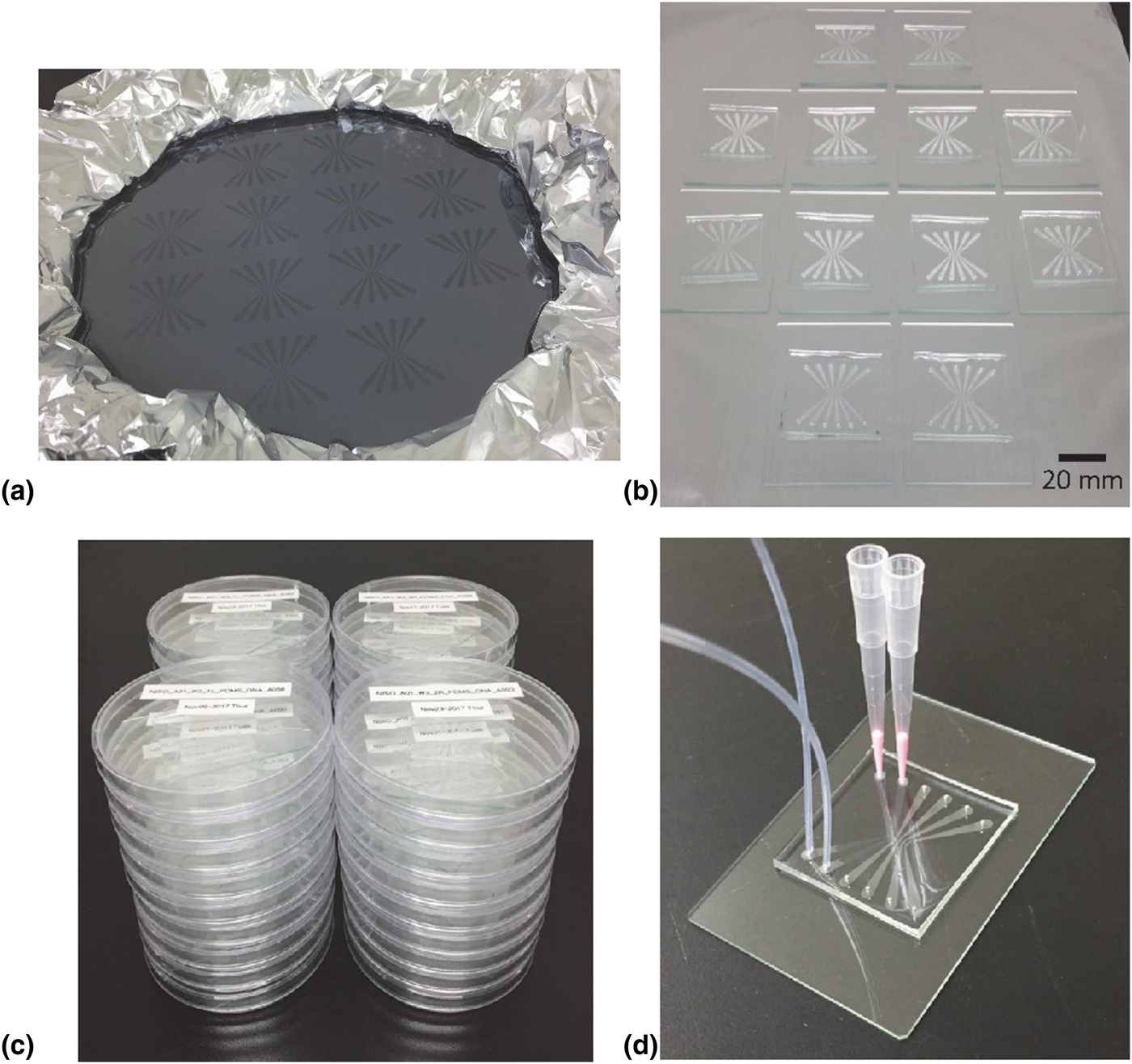
To explore the capability of mass production, we repeatedly performed the PDMS fabrications based on the given nanoscallop Si mold structure, as described in Fig. 2. Figure 2(a) shows the cured PDMS upon the 200 mm Si-wafer mold that is located inside an aluminum foil fence. From one piece of 200 mm Si-wafer mold, we were able to produce 12 pieces of PDMS chamber. Each PDMS chamber was shaped by a cutter and assembled with a slide glass as shown in Fig. 2(b). The assembled PDMS–slide glass devices were packaged in Petri dishes and labeled, as shown in Fig. 2(c). For the usage of the PDMS device, we connected the device with pipette tips at one side of the chamber and perfluoroalkoxy (PFA) tubes at the other side to form a fluidic circuit, as shown in Fig. 2(d).
A 200 mm wafer-scale fabrication of PDMS. (a) PDMS mixture solution is poured upon a 200 mm wafer located inside aluminum foil fence. (b) In one piece of the Si-wafer mold, 12 PDMS chambers are produced. After curing, peeling-off, cutting, hole-punching, and surface-activating procedures, each PDMS chamber is assembled with slide glass. (c) The assembled PDMS–slide glass devices are packaged and stored in Petri dishes. (d) Tubing and pipetting of each PDMS device enable microfluidic experiments.
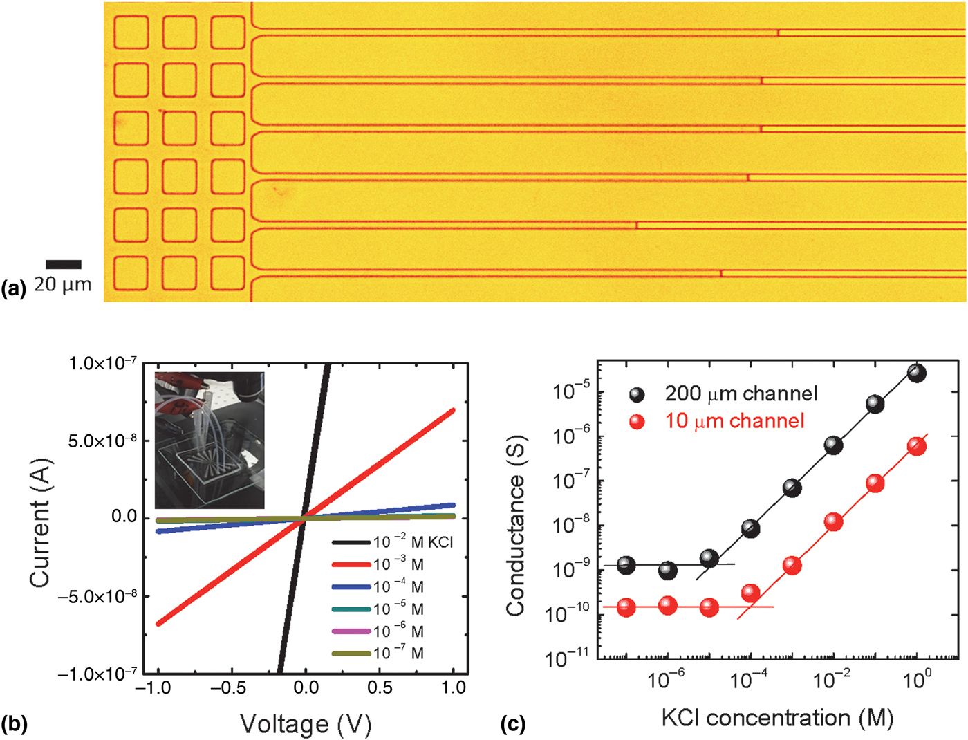
To validate the performance of the microfluidic devices, we examined physical properties of the channel such as electrical characteristics as shown in Fig. 3. Figure 3(a) is an optical microscopy image, which shows the center region of the fabricated PDMS chamber where 5 µm size channels are located. By inserting KCl electrolyte solution into the channels, we identified that the channels are slowly wetted from the left side of the chamber toward to the right side by displaying the meniscus of the liquid, as shown in Fig. 3(a). For better wetting of the KCl electrolyte solution, we sometimes mix the KCl electrolyte solution with ethanol or acetone. However, the aid of syringe pumping facilitates the wetting process of the microchannels, regardless of the charge status of the liquid whether it is a polar solvent or a nonpolar solvent. Figure 3(b) shows current (I)–voltage (V) characteristics of the PDMS microfluidic channels that are filled with the KCl electrolyte with the different concentrations from 10−7 to 10−2 M. The inset of Fig. 3(b) is a picture of a configuration of the electrical circuit of the microfluidic device connected with Ag/AgCl electrodes. Linear I–V character was identified, as shown in Fig. 3(b), which implies good Ohmic properties.
Wetting property and electrical characterization of the PDMS microfluidic channels. (a) Optical microscope image displays the channel-wetting behavior from the left side of the chamber toward the right side. The meniscus of the liquid is identified. Each channel has 5 µm size. (b) Current (I)–voltage (V) characteristics for different KCl concentrations from 10−7 to 10−2 M. (Inset) Experimental setup for electrical characterization of the PDMS chambers. (c) A plot of channel conductance as a function of KCl concentration for 10 µm channel (red dots) and 200 µm channel (black dots). Bulk conductance character is identified at high concentration, while the conductance is saturated at low concentration implying a surface-charge-governed ion-transport character. The crossing point c cross of the bulk conductance regime and the surface-charge-governed regime is identified as 10−4 M (for 10 µm channel) and 10−5 M (for 10 µm channel).
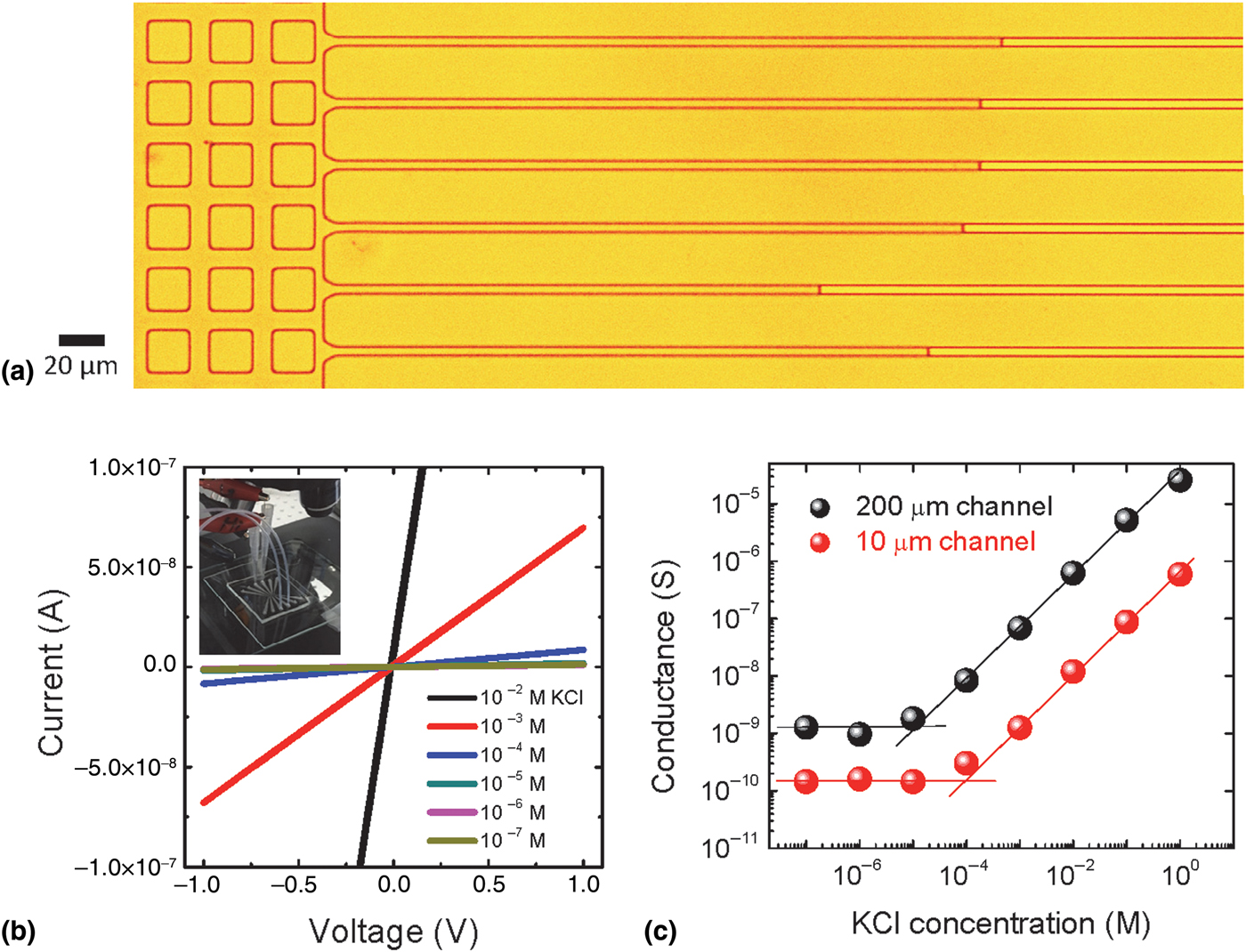
Figure 3(c) shows a plot of the channel conductance as a function of the KCl electrolyte concentration. At the higher concentration regime, the measured conductance increases linearly with the KCl concentration, implying a bulk conductance property. However, at the lower KCl concentration regime, the conductance is saturated at a certain KCl concentration, which is attributed to a surface-charge-governed ion transport. Since the electrical double layer (EDL) overlaps as the channel size decreases by the Debye length, the counter-ions blocking the surface charge fill most of the channels and control the ion transport by showing unipolar transport behavior.[Reference Stein, Kruithof and Dekker15–Reference Nam, Lee, Lee, Lee, Rossnagel and Kim18] According to the EDL-overlapping model, the crossing point of the bulk conductance and the surface-charge-governed conductance offers an information regarding the surface charge density, σ, which is expressed as
 $$\sigma = {\rm 1}0^{\rm 3}e{\rm} N_{\rm A}c_{{\rm cross}}d^{*}/{\rm 2}$$
where e is the elementary electric charge, N A is the Avogadro's number, c cross is the KCl concentration of the crossing point between bulk conductance and the surface-charge-governed conductance, and d* is the critical dimension of the fluidic channels.[Reference Nam, Rook, Kim and Rossnagel17] We compare the σ of the fabricated PDMS channels having ~10 µm critical dimension with that of ~200 µm big channels. The c cross of both 10 µm [red dots in Fig. 3(c)] and 200 µm channel [black dots in Fig. 3(c)] is 10−4 and 10−5 M, respectively. Based on these values, the σ values are calculated as 0.096 and 0.048 C/m2, respectively. This estimate allows us to verify that the σ of the PDMS chamber described in this report has a range of 10−1–10−2 C/m2, which is in good agreement with the values reported in the literature.[Reference Schrott, Slouka, Cervenka, Ston, Nebyla, Pribyl and Snita19, Reference Wong and Ho20]
Along with the reliable fabrication of microfluidic chambers, the ability to visualize single particles or single molecules is an important issue. Recently, fluorescence imaging technology of single DNA molecules has been used in genomic mapping technology in which chemical binding sites are specifically identified along the DNA strands by fluorescent labels.[Reference Cao, Tegenfeldt, Austin and Chou21–Reference Macosko, Basu, Satija, Nemesh, Shekhar, Goldman, Tirosh, Bialas, Kamitaki, Martersteck, Trombetta, Weitz, Sanes, Shalek, Regev and McCarroll26] In addition, Yelleswarapu et al. reported a microfluidic device equipped with a mobile phone camera in order to visualize and trace the single PS particles.[Reference Yelleswarapu, Jeong, Yadavali and Issadore27–Reference Wi, Park, Kang, Jung, Lee and Lee29] Also, physical control over the motions of single molecules or particles is of a fundamental importance.[Reference Keyser, Koeleman, Dorp, Krapf, Smeets, Lemay, Dekker and Dekker30, Reference Bai, Wang, Nam, Peng, Bruce, Gignac, Brink, Kratschmer, Rossnagel, Waggoner, Reuter, Wang, Astier, Balagurusamy, Luan, Kwark, Joseph, Guillorn, Polonsky, Royyuru, Rao and Stolovitzky31]
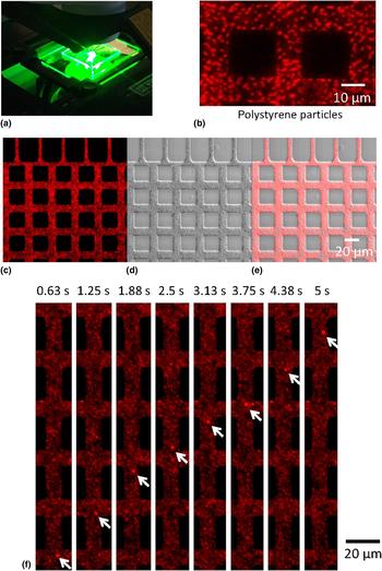
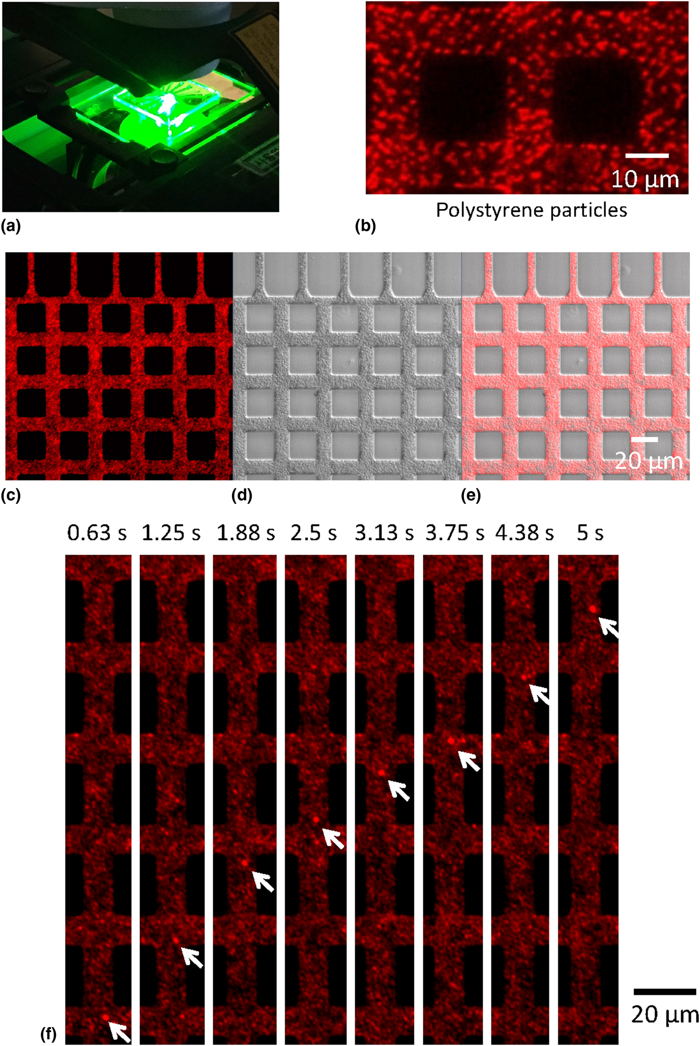
To visualize the motions of either single particles or single molecules, we introduce a confocal microscopy by coupling it with the fabricated PDMS chamber, as shown in Fig. 4(a). We tested imaging of an individual fluorescence PS particle having the diameter of ~500 nm. After inserting the PS particle solution into the PDMS chamber and drying the solvent, we were able to obtain a fluorescence image of the PS particles located inside the PDMS microfluidic channel, as shown in Fig. 4(b). Apparently, the red-color fluorescence image was identified from the individual PS particles. Next, we examined imaging of the flowing particles dissolved in the solvent. Image resolution is interrupted to some extent by the light scattering of the liquid solvent as well as the Brownian motion of the particles drifting along the liquid flow. Laser scanning light-source of the confocal microscopy enables us to obtain two different-mode images at the same time: One is a fluorescence image in Fig. 4(c) and the other is a DIC image in Fig. 4(d) (see also Supplementary Movie S1). A gray-scale DIC image of Fig. 4(d) enhances the contrast of the particle morphology.[Reference Schermelleh, Heintzmann and Leonhardt32–Reference Wang, Sun, Luo and Fang34] By overlapping both fluorescence and DIC images, as shown in Fig. 4(e), we were able to trace the motions of the particles more clearly. In Fig. 4(f), the snapshot of Supplementary Movie S1 shows a directional drifting motion of an individual particle.
Real-time imaging of single polystyrene (PS) particles by confocal microscopy. (a) Experimental setup of fluorescence confocal microscopy coupled by the PDMS chamber. (b) Fluorescence image of PS particles in the dry state. Individual particles are identified. (c–e) A captured image of Supplementary Movie S1, consisting of (c) fluorescence image, (d) differential interference contrast (DIC) image, and (e) the combined image of (c) and (d). (f) Movie illustrating a drifting motion of the single PS particle indicated by white arrows.
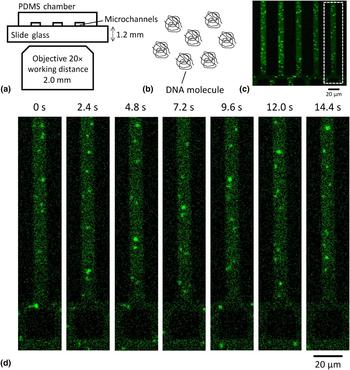
To visualize the motions of single DNA molecule inside the fabricated PDMS chambers, we prepared a solution in which λ-DNA molecules are stained by the YOYO-1 dye. Owing to the relatively thick ceiling height, PDMS (or slide glass) is regarded as being difficult to be coupled with oil-immersion objective or high-resolution power objective.[Reference Huh, Mills, Zhu, Burns, Thouless and Takayama5, Reference Yang, Moore, Schmidt, Klug, Lipson and Erickson6] To trade off this issue, researchers have used Pyrex borosilicate glass for wafer bonding or very thin Si-oxide layers for genome mapping and single DNA imaging.[Reference Wang, Nam, Cotte, Jahnes, Colgan, Bruce, Brink, Lofaro, Patel, Gignac, Joseph, Rao, Stolovitzky, Polonsky and Lin12, Reference Levy, Mannion, Cheng, Reccius and Craighead13, Reference Cao, Tegenfeldt, Austin and Chou21–Reference Bakajin, Duke, Chou, Chan, Austin and Cox24] In our case, however, we explore a capability of the fabricated PDMS chamber to image single DNA molecules. We optimized the optic system as illustrated in Fig. 5(a). The assembled PDMS–slide glass device is located upon the objective lens of the inverted microscope. The thickness of slide glass is 1.2 mm, thereby we used an objective lens that has a FWD of 2.0 mm. To obtain high magnification condition, a strategy is as follows: We used 20 × magnification objective lens with the PMT detector having 10 × magnification. In the image-processing software, we obtained 2 × magnification condition, thus obtaining 400 × nominal magnification which is suitable for single DNA molecule imaging. It is worth noting that the method described in this report suggests a protocol to achieve single molecular resolution in a conventional PDMS chamber.
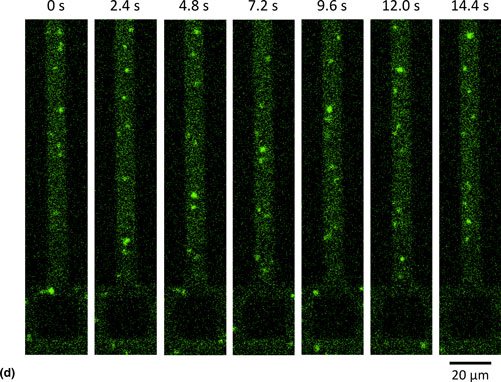
Real-time visualization of the motions of single DNA molecules flowing inside the fabricated PDMS chamber. (a) An experimental schematic of the assembled PDMS–glass device placed upon the inverted confocal microscopy with objective lens 20 × magnification. (b) An illustration of coil shape λ-DNA molecules. (c) A fluorescence image of single DNA molecule flowing along the 10 µm channels. (d) Time-elapse snapshots of Supplementary Movie S2 in the reduced area of the white rectangle in (c). From bottom to top, YOYO-tagged 48.5 kbp λ-DNA molecules are flowing with the velocity of 8.6 µm/s.
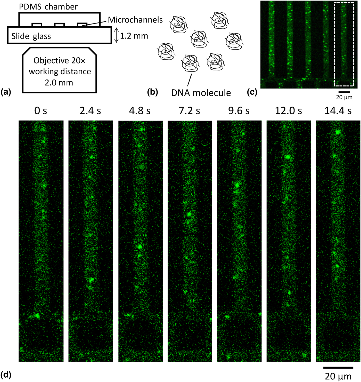
To wet the fabricated PDMS channels, we used a syringe pump to induce the flow of the λ-DNA solution into the channel region. The λ-DNA strand has 48.5 kilobase pair (kbp) long, thus having a coil shape, as shown in Fig. 5(b), to meet the condition of minimizing entropic energy.[Reference Bakajin, Duke, Chou, Chan, Austin and Cox24] Fig. 5(c) shows a snapshot of the YOYO-1-stained DNA single molecules flowing inside the fabricated PDMS chamber of 10 µm channel size. Supplementary Movie S2 shows a dynamic flow of the coil shape DNA single molecules. In the white rectangle region in Fig. 5(c), time-lapse images of the λ-DNA molecules flowing through the PDMS channel are shown in Fig. 5(d). Each frame was taken every 2.5 s, and the velocity of DNA flow in the PDMS device is measured as 8.6 µm/s.
In conclusion, we demonstrated real-time fluorescence imaging of single DNA molecules in a fabricated PDMS microfluidic channel. For reliable, reproducible, and recyclable fabricating systems, we build 200 mm Si-wafer mold in which “mesa”-type Si structure has the sidewall profile with nanoscallop geometry. The scallop geometry facilitates a residue-free peel-off process of PDMS, which offers a rapid and clean fabrication method of PDMS microfluidic channels. Based on the fabricated PDMS chambers, we optimized an optic system to visualize the motions of single DNA molecules. An advantage of this approach is the ability not only to fabricate PDMS chambers reliably but also to image single molecules in a real-time manner, which is in principle applicable for mass-production of biomedical devices to visualize single particles, proteins, and single-cell structures.
Supplementary material
The supplementary material for this article can be found at https://doi.org/10.1557/mrc.2018.58
Acknowledgment
This work was supported by KNU research fund 2016.