I. INTRODUCTION
A key feature in modern mobile communication is the variety of services simultaneously available to the end users, most requiring fast internet connection. This implies constantly increased data-rates to comply with the rising demand for new services. However, due to the limited bandwidth available for mobile applications, the adoption of spectral efficient modulations becomes mandatory. Unfortunately, these schemes are characterized by variable envelope and high peak-to-average power ratio (PAPR), making it crucial to adopt design architectures able to provide high efficiency in wider power ranges without compromising system linearity [Reference Bhushan1]. These requirements impact on the design and implementation of each system element, but in particular on the power amplifier (PA), one of the most non-linear and power-consuming modules of the transceiver [Reference Colantonio, Giannini and Limiti2, Reference Kenington3].
Among the proposed PA solutions, the Doherty power amplifier (DPA) is becoming very popular, thanks to its relatively simple architecture and good back-off efficiency [Reference Camarchia, Pirola, Quaglia, Jee, Cho and Kim4, Reference Kim, Moon and Kim5]. On the other hand, the relatively low linearity of the scheme, especially in terms of AM/PM conversion, makes it mandatory the adoption of linearization blocks based on e.g. predistortion or feedforward [Reference Ghannouchi and Hammi6]. While the combination of linearizer and DPA has been proved successful in mobile base station applications, in the mobile backhaul scenario the situation is different. Base stations, in fact, work at frequencies up to 4 GHz, with relatively narrow bandwidths and high power levels up to hundred of watts. In backhaul, instead, center frequencies and bandwidths are higher [Reference Little7], while the power levels are limited to 10–15 W in the lower bands, and further reduce at higher frequencies. The backhaul market is currently dominated by GaAs monolithic microwave integrated circuits (MMIC) combined class-AB PA (AB-PA), while it is still an open question if the adoption of more costly technologies, like GaN [Reference Camarchia8, Reference Reveyrand9], and/or more complex architectures, like the DPA, are justified by the expected efficiency increase [Reference Camarchia10, Reference Kistchinsky11]. As a matter of fact, the clear advantages theoretically given by these solutions are reduced by the need of more complex (and possibly more energy eager) linearization schemes.
Aim of this work is to provide a careful comparison of class-AB and DPA architectures for microwave backhaul. For this purpose, we designed and characterized two MMIC PAs, adopting the same GaN technology and device periphery, and targeting the same requirements: 7 GHz center frequency, 700 MHz bandwidth, 10 W saturated output power and a level of linearity (after applying the simplest possible predistortion scheme) sufficient to guarantee compliance with the emission mask of the reference standard for this application [12, 13].
The design details of both PAs are reported and discussed in Section II, while continuous wave (CW) characterization results are shown in Section III. Section IV reports the experimental results under modulated signal and, finally, Section V draws some conclusions. This paper is an expanded version of [Reference Giofré14] in which the preliminary results of the comparisons have been discussed.
II. POWER AMPLIFIERS DESIGN
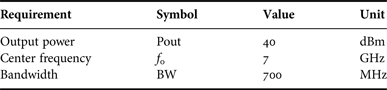
The main requirements of both PAs are listed in Table 1.
PAs specifications.
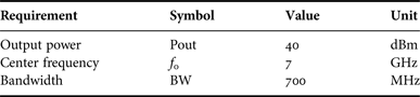
The center frequency is fixed at 7 GHz, targeting 10% of fractional bandwidth (700 MHz) and 10 W (40 dBm) of saturated output power.
The selected technology is the GH25-10 GaN process by United Monolithic Semiconductor. It is a 0.25 µm gate length HEMT (high-electron-mobility transistor) process, providing a power density of about 3 W/mm at 25 V of drain voltage. Theoretically, this yields to a minimum total periphery of 3.3 mm to reach the required output power, a figure that however must be slightly increased to account for the losses introduced by the output combiner, necessary in both architectures.
The gate periphery choice is limited to the active device sizes for which non-linear models are available. Consequently, the active devices selected for both PAs are 8 × 130 µm gate-periphery HEMTs. These devices show, at 7 GHz, ~3 W output power when biased in class-AB, i.e. V DD = 25 V, V GG = −3.2 V and I D = 33 mA. Four devices (4 × 8 × 130 µm total periphery) are used in both designed PAs to achieve the target output power.
A) Combined class-AB PA
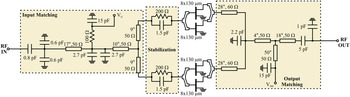
The electrical scheme of the AB-PA is reported in Fig. 1. The four active devices are combined in two pairs, forming two macro-cells each with a total periphery of 16 × 130 µm. The two macro-cells are stabilized with a parallel R-C filter in series to the gates, which values (200 Ω and 1.5 pF) have been optimized to guarantee broadband unconditional stability, and minimum in-band insertion loss. The macro-cell is matched to the external 50 Ω termination both at the output, targeting best compromise between output power and efficiency, and at the input, where conjugate matching condition is enforced.
Schematic of the combined class-AB PA.

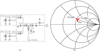
The output matching network of the AB-PA has been designed according to a semi-lumped strategy (see Fig. 2(a)), where each element has been carefully optimized through extensive non-linear simulations. Note that the real part of the 16 × 130 µm macro cell optimum load is close to R OPT = 50 Ω. As shown in Fig. 2(b), the load synthesized by the combining network is close to this value on a good bandwidth. The drain bias voltage of all devices is provided from a single supply point (V DD ) through a 50° (at center frequency) transmission line.
(a) Schematic of the output matching network of the combined AB-PA, including devices’ equivalent output circuits. (b) Synthesized load.

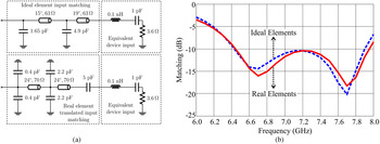
The semi-lumped approach has also been adopted for the input matching network reported in Fig. 3(a), where a low-pass ladder network implements the impedance transformation. In particular, Fig. 3(a) compares the ideal element network and its translation to real elements (metal insulator metal capacitors and microstrip transmission lines), together with the obtained matching. Differences from ideal to real elements are due to the effects of discontinuities and via holes in the MMIC implementation. The realized capacitors have a nominal capacitance lower than the theoretical one, and lines result longer for the insertion of the 5 pF DC-block capacitor. The gate bias voltage, fed from a single supply V G , has been applied through a 100 Ω resistor and low-pass filtered.
(a) Schematic of the input matching network of the AB-PA, with ideal elements (upper) and the translation to real components (lower), including devices’ equivalent input circuits. (b) Simulated matching.

A microscope picture of the realized AB-PA is reported in Fig. 4. The chip size is 3 × 3 mm2, but it is worth to note that the module footprint is only 2/3 of this area.
Microscope picture of the combined class-AB PA. Size is 3 × 3 mm2.

B) Doherty power amplifier
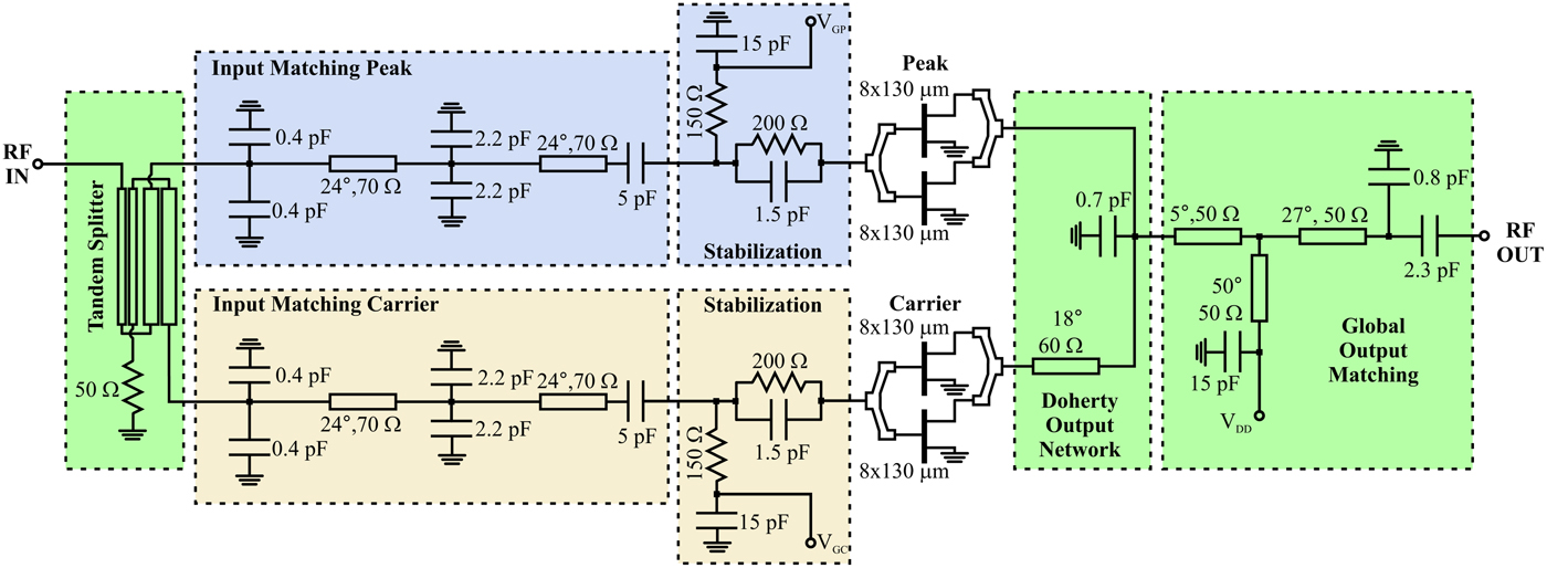
The electrical scheme of the DPA is reported in Fig. 5. The same elementary macro-cell (two 8 × 130 µm2 devices) has been used for carrier and peak amplifiers, in combination with the same parallel R-C stabilization network employed in the AB-PA.
Schematic of the Doherty PA.
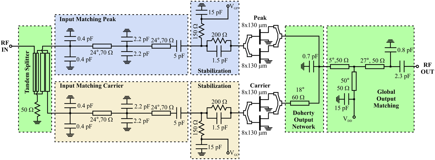
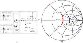
Figure 6(a) shows the output matching network of the DPA: the impedance inverter network inserted between the common node and the carrier device for load modulation [Reference Giofré, Piazzon, Colantonio and Giannini15] has been synthesized through a Π-network given by the devices’ output capacitance and a line with 18° electrical length at f 0. As for the AB-PA, the drain bias voltage is applied from a single supply point through a short circuit stub with 50 Ω impedance and 50° electrical length at center frequency. The external 50 Ω termination is transformed, at the common node between carrier and peak cells, in the optimum resistance R OPT /2 = 25 Ω through the output global matching network, which is implemented in semi-lumped form, exploiting a C-L-C Π-network. Finally, a DC-block of 2.3 pF has been inserted. The modulation of the synthesized load is shown in Fig. 6(b).
(a) Schematic of the output matching network of the DPA, including devices’ equivalent output circuits. (b) Synthesized load modulation.

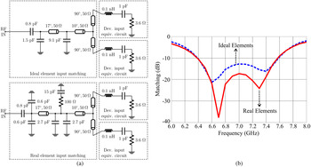
Figure 7, which shows the input matching network adopted for both carrier and peak devices, compares the first schematic obtained with ideal elements to that obtained after optimization with real components.
(a) Schematic of the input matching network of the DPA, with ideal elements (upper), and the translation to real components (lower), including devices’ equivalent input circuits. (b) Simulated matching.

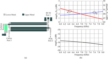
A tandem coupler is adopted as input power splitter, see Fig. 8(a) [Reference Shelton and Mosko16]. Given the technological constraints in terms of minimum line widths and distance between lines, the tandem coupler resulted more effective than a Lange coupler, ensuring better isolation between branches. The final layout is adjusted through electromagnetic simulations, and its simulated performance is shown in Fig. 8(b).
(a) Layout of the tandem coupler used as input splitter of the DPA. (b) Magnitude and phase of splitting ratio (upper) and input matching (lower).

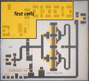
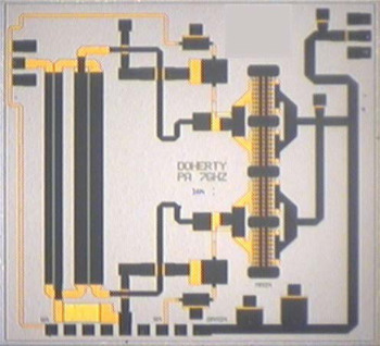
A microscope picture of the realized DPA is reported in Fig. 9. In this case, the DPA needs a larger area (about 30%) than the AB-PA, mainly due to the input splitter size. Indeed, the same 3 × 3 mm2 chip area is fully occupied by the circuit: this is an aspect that has to be considered for the final cost of the chip.
Microscope picture of the DPA.

III. SMALL SIGNAL AND CW CHARACTERIZATION
The drain bias voltage is fixed to 25 V for both PAs. A class-AB bias point, corresponding to V G = −3.2 V and I D = 120 mA, is selected for the AB-PA and for the carrier amplifier of the DPA, while the peaking amplifier is biased in class-C, setting V G, P = −5.2 V.
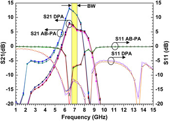
Small signal characterization has been carried out between 1 and 15 GHz. Figure 10 shows the measured scattering parameters of both MMICs at the nominal bias point. Some samples of each PA have been measured, denoting small impact of process variations on the design. The small signal gain of the AB-PA is around 11 dB, while that of the DPA is 7 dB. In terms of input return loss, the DPA shows better performance than the AB-PA, thanks to the presence of the tandem coupler at the input. However, in the targeted bandwidth, the S 11 of the AB-PA is always lower than −8 dB.
Measured scattering parameters of both MMICs.

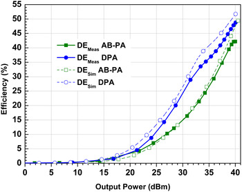
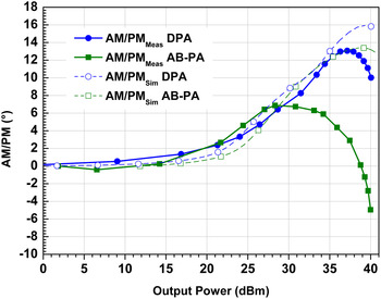
The MMICs have been then characterized in large signal condition at different frequencies. For both PAs, the comparison between measured and simulated drain efficiency, amplitude (AM/AM) and phase (AM/PM) distortion at center frequency (7 GHz) is reported in Figs 11–13.
Comparison between simulated and measured efficiency as a function of the output power at 7 GHz.

Comparison between simulated and measured AM/AM as a function of the output power at 7 GHz.

Comparison between simulated and measured AM/PM as a function of the output power at 7 GHz.

As expected, thanks to the early saturation of the carrier device, the DPA shows higher efficiency in back-off.
At saturation, the lower efficiency of the AB-PA is not intuitive. In theory, since the two PAs have the same active periphery, they work in similar conditions. However the peak macro-cell of the DPA module is biased in class-C with a lower average current than the AB-PA devices, and hence its temperature remains lower. This contributes to the better saturated performance of the DPA.
In terms of amplitude distortion, the DPA shows better behavior than the AB-PA. In fact, thanks to the boosting effect of the peak cell, the AM/AM of the DPA is not affected by the soft-compression phenomenon that is, instead, exhibited by the AB-PA, as clearly stated in Fig. 12. Concerning the AM/PM conversion, it is not clear which is the preferred solution along the overall output power range (see Fig. 13). In fact, both PAs show similar behaviors from small signal up to roughly 6 dB of output power back-off (OBO), where the peak cell in the DPA turns on. For higher output power levels, the AM/PM of the AB-PA starts decreasing, reaching a final value around −6°. On the contrary, in the so-called “Doherty region”, i.e. where both carrier and peak devices are active, the phase distortion of the DPA rises up to a maximum value of 13°. This different AM/PM trend in a DPA is due to the contribution of the load modulation, as demonstrated in [Reference Piazzon17].
The measured output power and drain efficiency at both 6 dB back-off and saturation, as a function of frequency between 6.7 and 7.3 GHz, are reported in Fig. 14. In the specified bandwidth, the saturated output power is around 40 dBm for both PAs, while the measured back-off efficiency of the DPA is 50% higher than that of the AB-PA (36% versus 24%).
In-band CW characterization: saturated output power, drain efficiency at saturation and at 6 dB OBO.

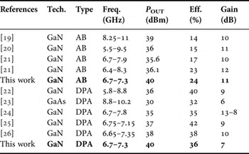
Table 2 compares the performance of these MMICs with recent literature examples of other class AB and Doherty PAs conceived for similar applications. Both PAs show higher output power with respect to other works, while assuring similar levels of efficiency.
Performance comparison of recently published PAs for radio links.

Bold font is used to highlight the results of the present work. DPA: Doherty power amplifier; AB, Class AB; Eff. refers to 6 dB output power back-off.
IV. SYSTEM LEVEL CHARACTERIZATION
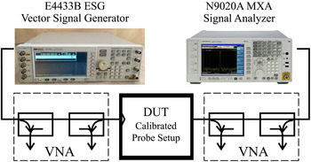
The linearity of the two MMICs has been tested adopting a 256 QAM (quadrature amplitude modulation) signal with a 28 MHz channel and 7.2 dB of PAPR at the center frequency of 7 GHz. The European Telecommunications Standards Institute (ETSI) spectrum emission mask 6LA has been adopted as a reference [12, 13]. Figure 15 shows the basic system level characterization and DPD test bench, with the most significant components. The adopted Signal Generator (SG) is the Agilent E4433B ESG and the Vector Signal Analyzer (VSA) is the Agilent N9020A MXA. For amplifier characterization, the baseband signal is passed to the SG and modulated, then fed to the device under test (DUT) and finally recollected, after amplification, by the VSA. A Matlab software installed in an external PC controls both the SG and the VSA. For accurate on-wafer measurements of the output power and efficiency, the bench has been pre-calibrated following the approach described in [Reference Quaglia, Tao and Vittorio18] to correctly relate the absolute power at the VSA with the power at PA level, in our case at the MMIC reference planes.
Measurement setup for system level characterization and predistortion.

Both amplifiers have been biased in the same conditions adopted for the CW characterization, (V DS = 25 V, V G = −3.2 V, I D = 120 mA for class-AB devices, V GP = −5.2 V for the class-C DPA peak device).
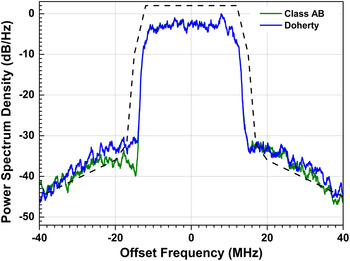
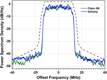
In Fig. 16 the measured output spectrum of the two amplifiers at 33 dBm output power (7 dB from saturation) is shown. As predicted by the static AM/AM and AM/PM characteristics, the linearity requirements are not satisfied by the amplifiers alone, with a lower spectral regrowth shown by the AB-PA.
Measured output spectrum of the AB-PA (green line) and DPA (blue line) MMICs without predistortion compared with ETSI emission mask 6LA (black line). Test signal is a 256 QAM, 28 MHz channel. The average output power is 33 dBm.

To achieve mask compliance, a digital predistortion (DPD) scheme based on a memory polynomial model has been adopted, using 6th order odd polynomial and two memory taps for both PAs. Figure 17 reports the results obtained after predistortion. The different AM/AM and AM/PM behavior between the two stages leads to larger margin from the emission mask in the AB-PA case, achieved using a back-off practically equal to the PAPR, i.e. average output power of 33.6 dBm. For the DPA, the back-off required to respect the emission mask is slightly higher, i.e. average output power of 32.3 dBm, and almost no margin is present. On the other hand, the average efficiency of the DPA is 33%, i.e. 10 percentage points higher than that of the AB-PA.
Measured output spectrum of the AB-PA (green line) and DPA (blue line) MMICs with predistortion (6th order odd polynomial, 2 memory taps) compared with ETSI emission mask 6LA (black line). Test signal is a 256 QAM, 28 MHz channel. Average output power is 33.6 dBm for the AB-PA and 32.6 dBm for the DPA. The resulting average efficiencies are 24 and 33%, respectively.

V. CONCLUSIONS
A comprehensive comparison between a combined AB-PA and a DPA for microwave backhaul applications has been presented. The two PAs, fabricated in a 0.25 µm GaN MMIC technology, have been designed to work at 7 GHz, considering 10% fractional bandwidth, and targeting 40 dBm output power. The efficiency-linearity trade-off of both architectures has been addressed through a relevant experimental characterization, and pros and cons of each solution have been discussed. The results show that both circuits fulfill the output power and bandwidth requirements. The DPA has demonstrated a higher efficiency both at saturation and at 6 dB output power back-off, than the class-AB, however at the expense of lower linearity and larger chip area. As a summary, we can conclude that DPA architectures can be potentially adopted in microwave backhaul nodes in place of AB-PAs, but higher production costs and possible linearity issues have to be accounted for.
 Rocco Giofré received the Electronic Engineering degree (M.S. Eng.), summa cum laude, from University of Roma “Tor Vergata” in 2004 and the Ph.D. degree in Space Systems and Technologies in 2009 from the same University. He is presently an Assistant Professor at the University of Roma “Tor Vergata”. His research interests include RF power amplifier theory, design and test, linearization and efficiency improving techniques. He was the recipient of the 2005 Young Graduated Research Fellowship presented by the GAAS Association and of the best paper award at the 2th EuMIC Conference in 2007. He has authored or co-authored over 120 scientific papers.
 Paolo Colantonio was born in Roma, Italy on March 22, 1969. He received the Electronic Engineering degree and Ph.D. degree in Microelectronics and Telecommunications from the University of Roma “Tor Vergata”, Italy, in 1994 and 2000, respectively. In 1999 he became a Research Assistant with the University of Roma “Tor Vergata”, where, since 2002, he has been a Professor of Microwave Electronics. He authored or co-authored more than 200 scientific papers. He authored the book High Efficiency RF and Microwave Solid State Power Amplifiers (Wiley, 2009). His main research activities are in the field of nonlinear microwave circuit design methodologies, nonlinear analysis techniques, and modelling of microwave active devices.
 Franco Giannini was born in Galatina (LE) Italy, on November 9, 1944. He received the Electronics Engineering degree (summa cum laude) from the University of Roma “La Sapienza,” Rome, Italy, in 1968. Since 1980, he has been a Full Professor of applied electronics with the University of Rome Tor Vergata, Rome, Italy. Since 2001, he has been an Honorary Professor with the Warsaw University of Technology (WUT), Warsaw, Poland. He has been involved with problems concerning modelling, characterization, and design methodologies of linear and nonlinear active microwave components, circuits, and subsystems, including monolithic microwave integrated circuits (MMICs). He is a consultant for various national and international industrial and governmental organizations, including the International Telecommunication Union and the European Union. He has authored or co-authored over 430 scientific papers. Prof. Giannini is a member of the Board of Directors of the Italian Space Agency (ASI). He is the president of the GAAS Association. He has also been a member of numerous committees of international scientific conferences. He was the recipient of the Doctor Honoris Causa degree from the WUT in 2008.
 Chiara Ramella was born in Biella, Italy in 1985. She received the M.S degree in Electronic Engineering and the Ph.D. degree in Electronic Devices from Politecnico di Torino in 2009 and 2013, respectively. She is currently working as research assistant at University of Rome Tor Vergata in collaboration with Politecnico di Torino. Her research activities spread from low-noise analog electronic design to RF/microwave design and measurements.
 Vittorio Camarchia received the Laurea degree in Electronic Engineering and Ph.D. degree in Electronic and Communications Engineering from the Politecnico di Torino, Turin, Italy, in 2000 and 2003, respectively. In 2001, 2002, and 2003, he was a Visiting Researcher with the Electrical and Computer Engineering Department, Boston University, Boston, MA. He is currently an Associate Professor of electronics with the Electronics and Telecommunication Department, Politecnico di Torino, Turin, Italy. His research is focused on the design and experimental characterization of hybrid and integrated circuits and systems for microwave RF applications both linear and non-linear (scattering, source/load-pull technique, system level characterization) and large signal circuit and system level modeling of microwave power devices. He is the author or co-author of around 120 technical publications in journal papers and conference proceedings plus two book-chapters and many technical reports.
 Mustazar Iqbal received the B.S. and M.S. degrees in Electronic Engineering from BUITEMS, Pakistan and Dongguk University Seoul, Korea, in 2011 and 2013, respectively. He is currently working towards the Ph.D. degree at the Politecnico di Torino, Italy. His current research interests concern the design and simulation of high-efficiency power amplifiers.
 Marco Pirola was born in Velezzo Lomellina, Italy, in 1963. He received the Laurea degree and Ph.D. in Electronic Engineering from Politecnico di Torino, Turin, Italy, in 1987 and 1992, respectively. In 1992 and 1994, he was a Visiting Researcher with the Hewlett Packard Microwave Technology Division, Santa Rosa, CA. Since 1992, he has been with the Department of Electronics and Communications, Politecnico di Torino, Turin, Italy, first as a Researcher and, since 2000, as an Associate Professor, where his research concerns the simulation, modeling, desing, and measurements of microwave devices and systems.
 Roberto Quaglia received the Laurea degree and the Ph.D. from Politecnico di Torino, Italy, in 2008 and 2012, respectively. He has been a visiting Ph.D. student at Chalmers University, Sweden, working on reconfigurable microwave circuits. From 2012 to 2014, he has been a Post-Doc fellow at the Department of Electronics and Telecommunications at Politecnico di Torino, where he carried out his research on microwave power amplifiers theory, design and characterization. In 2015 he worked for Huawei Technologies in Milano, Italy, as a MMIC designer for millimeter-wave radios. He is currently a researcher at the Centre for High Frequency Engineering at Cardiff University, working on the research project PADWIC on high efficiency broadband power amplifiers, supported by the European Union's Horizon 2020 research and innovation programme under a Marie Skłodowska-Curie grant agreement.