Introduction
In modern fifth-generation (5G) mobile communication applications, smartphone antenna design presents increasing challenges. This is primarily due to the growing number of operating frequencies, including new 5G bands, multi-input multi-output (MIMO), and carrier aggregation (CA), all of which necessitate multiple antennas operating simultaneously [1, Reference Li, Gao and Han2]. To achieve antennas with wider bandwidth operation and reduced power consumption, compact antenna tuner (AT) switches with low leakage current and high linearity are crucial.
Generally, antenna aperture tuning switches can encounter RF voltages exceeding 80 V when a cellular device operates at maximum transmitted power [Reference Özdamar, Hagelauer and Solomko3]. Therefore, these switches must exhibit a high breakdown voltage that surpasses the specific maximum voltage (V PEAK) of the AT, while also delivering acceptable harmonic performance. Insufficient V PEAK can lead to permanent, catastrophic damage to the AT. Furthermore, inadequate V PEAK can significantly degrade the AT’s isotropic sensitivity and radiated power, potentially generating undesired harmonic power. Consequently, Complementary Metal-Oxide-Semiconductor (CMOS)-based high-voltage RF switches, often composed of highly stacked RF MOSFET series, are widely employed in modern cellular phone antenna tuning switches [Reference Rigato, Fleury, Schwarz, Mergens, Bychikhin, Simbürger and Pogany4, Reference Solomko, Tayari, Essel and Weigel5].
The number of stacked RFCMOS devices is linearly proportional to the V PEAK and influences the total ON-state resistance (R ON) and OFF-state capacitance (C OFF). Stacking low-voltage RFCMOS transistors in series (e.g., over 20 transistors to achieve 80 V handling capabilities) introduces three primary issues:
1) The large silicon chip area required for highly stacked MOSFET switches leads to a corresponding increase in substrate capacitance (C sub).
2) Non-uniform RF voltage distribution along the MOSFET stack, due to V PEAK division among individual devices, amplifies odd-mode distortions.
3) A high total leakage current (I leak) shifts the MOSFET DC gate-source voltage, thereby degrading the switch’s RF breakdown voltage.
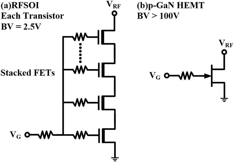
Addressing these considerations, an inverted-F antenna tuned by a 4-bit, high-voltage switchable capacitor implemented with an enhancement-mode (E-mode) p-GaN HEMT Monolithic Microwave Integrated Circuit was first demonstrated. A key advantage of E-mode p-GaN HEMT over traditional depletion-mode (D-mode) GaN HEMT is its direct compatibility with standard Mobile Industry Processor Interface power ICs used in smartphones. GaN-based switches are superior to other semiconductors like Si and GaAs due to their exceptional attributes, including high electron mobility, a large bandgap, high breakdown voltage, and excellent thermal conductivity [Reference Campbell and Dumka6–Reference Erturk and Ozbay8]. For a single-gate p-GaN HEMT switch with a gate length of 0.5 µm and a gate width of 0.2 mm, the OFF-state capacitance (C OFF) is 195 fF/mm, and the ON-state resistance (R ON) is 1.73 Ω · mm. The proposed GaN AT switch also achieves a hard breakdown voltage of 100 V and a 43 dBm power handling capability under 4 GHz operation. The p-GaN HEMT exhibits a higher breakdown voltage than traditional RFSOI, thereby precluding the necessity of stacked structures, as shown in Fig. 1.
The structure of antenna tuner: (a) RF SOI and (b) p-GaN HEMT.

Experimental procedures
The p-GaN HEMT epitaxial layers were grown on a 6-inch FZ high-resistivity (>8000 Ω-cm) Si substrate through metal organic chemical-vapor deposition. The cross-sectional image of the p-GaN HEMT switch is depicted in Fig. 2. To minimize source resistance and inductance, backside vias were implemented in this study. A 300 nm thick undoped GaN channel layer was grown on top of a 1.2 µm thick carbon-doped Al0.05GaN/GaN buffer/transition layer, followed by a 1 nm thick AlN spacer layer above the GaN channel. Afterward, a 12 nm thick Al0.22Ga0.78N layer and a 60 nm thick p-type GaN layer were grown with an Mg doping concentration of 1 × 1019 cm−3.
Cross-section of the p-GaN HEMT switch structure and SEM image of the fabricated p-GaN gate in the right-bottom corner.

Device fabrication commenced with the removal of the p-GaN stack outside the gate region using low-damage Cl2/BCl3/SF6-based inductively coupled plasma dry etch, followed by multi-condition N ion implantation for isolation. Ohmic contacts were prepared by electron beam evaporation, with Ti/Al/Ni/Au (25/125/55/125 nm) stacked sequentially on the device. The device was then annealed using an Rapid thermal annealing (RTA) system at 875 °C for 30 s in N2 ambient. Finally, a Ti/Au (50/350 nm) gate metal stack was deposited, and a 100 nm optimized atomic layer deposition grown film was deposited as a passivation layer. The fabricated device has gate length, gate-to-source, and gate-to-drain spacings of 0.8, 1.2, and 1.2 µm, respectively.
Results and discussion
The major limitation of the RF switch transistor is its drain-to-source breakdown voltage, which defines the voltage handling capabilities of a single transistor, nonlinear distortions, and gate-to-drain leakage, especially in deep sub-micron RFCMOS. As shown in Fig. 3(a), if the breakdown voltage is defined as the maximum applicable drain DC voltage before a sudden increase in drain current occurs, a hard breakdown voltage of 100 V with a gate-to-drain spacing of 1.2 µm is measured. For practical industrial AT switch usage, the DC breakdown is 20% higher than the RF maximum voltage swing, thus the proposed GaN device exhibits a sufficient breakdown voltage margin to handle an 80 V RF voltage swing [Reference Bordignon, Lucci, Fache, Pribat, Grégoire, Estellon, Monsieur, Guitard, Chalupa, Chevalier, Duriez and RF9, Reference Chan, Chen, Ko and Hu10].
(a) The off-state breakdown voltage (VBR). (b) I DS–V DS with V GS = 0, −1, −2 V, respectively.

During OFF-state operation of the AT switch, all 4-bit GaN HEMTs must operate in the cut-off region. Large RF voltage levels applied to the drain region of the p-GaN HEMT form a deep depletion region directly below the gate-drain access region, which may induce tunneling and surface hopping leakage currents. In Fig. 3(b), the OFF-state p-GaN HEMT I DS–V DS with V GS = 0, −1, −2 V are measured to verify the drain-voltage–induced leakage current. Unlike RFCMOS, bulk leakage current is not involved in this phenomenon due to the high-resistivity carbon-doped GaN buffer layer. With a drain voltage of 3 V, the I DS at V GS of 0 V is 0.1 A/mm in the p-GaN HEMT. This value is one order of magnitude lower than that of published RFCMOS AT switches, owing to its large bandgap (Eg = 3.4 eV) [Reference Rigato, Fleury, Schwarz, Mergens, Bychikhin, Simbürger and Pogany4, Reference Solomko, Tayari, Essel and Weigel5]. The leakage current can be further reduced to 1 nA/mm because the gate tunneling current is suppressed by the thicker gate depletion region under reverse gate bias at the p-GaN/AlGaN heterostructure. The low leakage current in the p-GaN HEMT switch is beneficial for low-power consumption mobile unit applications.
As shown in Fig. 4, a planar inverted-F antenna (PIFA) with RF voltage distribution along the antenna indicates that the internal impedance of the AT can be locally higher than 50 Ω. Thus, the V PEAK can reach 80 V when the antenna is fed with the maximum transmitted power. The 4-bit p-GaN HEMT AT was implemented by shunting four p-GaN HEMTs switched capacitors (0.25 pF), with individual HEMT gate widths of 0.2 mm. The p-GaN HEMT switch gate voltage pad is connected to the device gate electrode through a 2 kΩ 2-DEG resistor. The p-GaN HEMT AT achieves a compact chip compared to traditional stacked RFCMOS AT, making it suitable for the assembly form factor of smartphone radio frequency front-end (RFFE) modules.
The diagram of PIFA antenna with antenna aperture tuner and V PEAK effect of the tuning element location.

The measurement setup for the harmonic level and power handling capability is detailed in Fig. 5, for large signal measurements and to obtain Insertion Loss versus input Power data. The S-parameters of p-GaN HEMT ATs in OFF- and ON-states have been measured to ensure the proposed circuit PIFA module’s small-signal characteristics and power handling demands of the switch.
AT power handling and harmonic measurements block diagram.

The isolation and return loss with all switches in the OFF-state are shown in Fig. 6(a). Due to the compact switch size, the return loss exhibits less frequency dependency compared to the stacked RFCMOS architecture. In addition, the isolation is less than 15 dB up to 8 GHz. The insertion loss of 0.22 dB at 4 GHz in the RF SW1 ON-state is demonstrated in Fig. 6(b). By defining the output power exhibiting 0.1 dB degradation (P0.1dB) as the AT power handling capability, the P0.1dB is 44 dBm, which is 10 dB more robust than the 5G n77 band PA maximum output power. For large-signal measurements, an RF signal at 4 GHz was applied to the feed, and the continuous wave power was swept from 24 dBm up to 43 dBm. The amplitude of the RF voltage at the aperture tuning network reaches 60 V when the antenna is fed by a 34 dBm signal. The plots of H2 and H3 harmonics at 4 GHz are shown in Fig. 7(a), with values of −56 and −75 dBm, respectively. Benchmarking with a published high-voltage RFCMOS AT switch [Reference Gianesello, Monroy, Vialla, Canderle, Bertrand, Buczko, Coly, Nowakowski, Revil, Rolland and Gloria11], the performance achieved with a short gate width (Wg) device (Wg = 0.2 mm, 4 p-GaN HEMTs) is approximately 10 dB better for H3 in the ON-state (180 nm RFSOI, H3=-65dBm@Pin=34dBm). The switch’s odd-order nonlinearities are mainly generated by the nonlinear gate capacitances (C gs, C gd). Since these capacitances are proportional to the gate width of the HEMT, the improvement in odd-order nonlinearities in the p-GaN HEMT AT is due to its small gate capacitance. Additionally, the distorted RF voltage division of the stacked-FET architecture is another source of nonlinearity, which was negligible in single p-GaN HEMT. Figure 7(b) shows the return loss (S11) of the PIFA with p-GaN AT using a network analyzer. Four resonant frequencies are observed, with each reflecting a state of the switch. Each switching state connects a particular shunt capacitor to the tuning port of the antenna. Depending on the switched capacitor position, a significant improvement can be seen in the return loss at the desired frequency band. As shown in Fig. 7(b), the antenna tuning range covers the n77 (3.3–3.8 GHz) cellular frequency bands.
(a) The measured frequency-dependent isolation and return loss. (b) The insertion loss versus input power of p-GaN HEMT AT.

(a) The measured output power of H2 and H3. (b) The return loss (S11) of antenna with 4 states C-tuned AT switching.

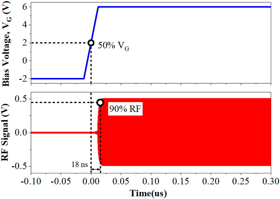
The comparison in Table 1 indicates that, at higher operating frequencies, this work achieves enhanced H3 performance and return loss, which can be attributed to the reduced stacking requirement and the p-GaN HEMT-based switch architecture. The switching time was measured at an RF frequency of 0.9 GHz. As shown in Fig. 8, a pulse voltage with an OFF-state of −2.5 V (0 V) and an ON-state of 6 V (0 V) was applied to the gate (body), featuring 50 ns rise and fall times. A 17 dBm RF input was applied, and the output RF signal was examined. The bias switching-on time was 18 ns. Based on the gate trap densities of RFSOI RF switches reported in references [12–Reference Özdamar, Weigel, Hagelauer and Solomko14], the trap density is on the order of ∼1011 cm−2 · eV−1, which can be attributed to the high-quality Si gate insulator/semiconductor interface. In contrast, the gate trap density of the p-GaN HEMT investigated in this study is approximately ∼1012 cm−2 · eV−1, with the dominant traps originating from the p-GaN/AlGaN junction interface within the ohmic–gate p-GaN HEMT structure. Despite the higher gate trap density, the off-state breakdown voltage of the p-GaN HEMT reaches 100 V, which is approximately one order of magnitude higher than that of RFSOI CMOS devices. As a result, RFSOI AT switches typically require a stacked transistor architecture to withstand high voltage reflections induced by rugged operating conditions. The gate switching time measurement results in Fig. 8, the proposed single-device p-GaN HEMT AT switch demonstrates switching performance comparable to that of commercial AT switch solutions.
Measurement results of the switching time at a 0.9 GHz of the RF frequency.

Comparison with other works

Conclusion
A high-voltage E-mode p-GaN compact-size AT switch with low leakage current is presented in this study. The form factor improvement is attributed to the high bandgap and high electric-field strength of the AlGaN/GaN heterostructure. Furthermore, the low insertion loss, high power handling, and low H3 are contributed by the low leakage current and low C OFF. The demonstration of the GaN-based AT switch provides insight into a next-generation, high-frequency antenna aperture tuner alternative solution.
Competing interests
The authors declare none.

Chia-Hao Yu received the M.S. degree in 2015 from the Department of Electronics Engineering, Chang Gung University, Taoyuan, Taiwan, where he is currently pursuing the Ph.D. degree. His research interests include RF circuit design for wireless communications, with a focus on microwave and millimeter-wave circuits and GaN-based RF power amplifiers.

Hsien-Chin Chiu (Senior Member, IEEE) received the Ph.D. degree in electrical engineering from National Central University, Zhongli, Taiwan, in 2003. He is currently a Professor with the Department of Electronic Engineering, Chang Gung University (CGU), Taoyuan, Taiwan, where he also served as the Director of High-Speed Intelligent Communication Research Center from 2012. He was invited to join the publicity and marketing team of the Adcom Committees Organization in the IEEE Microwave Theory and Techniques Society. He has authored or co-authored more than 230 SCI journal publications. His research interests include microwave, millimeter wave integrated circuits, GaAs and GaN FETs fabrication, and modeling. He is a member of Phi Tau Phi.

Chia-Han Lin received the M.S. degree in 2015 from the Department of Electronics Engineering, Chang Gung University, Taoyuan, Taiwan, where he is currently pursuing the Ph.D. degree. His main research area is RF circuit design, including applications in wireless and satellite communications.

Chong-Rong Huang received the M.S. degree in 2019 from the Department of Electronic Engineering, Chang Gung University, Taoyuan, Taiwan, where he is currently pursuing the Ph.D. degree. His research interests focus on III–V compound semiconductor devices, particularly GaN-based microwave and power devices.

Hsuan-Ling Kao received the B.S. degree in electrical engineering from Chang Gung University, Taoyuan, in 1998, and the M.S. and Ph.D. degrees in electronics engineering from National Chiao Tung University, Hsinchu, Taiwan, in 2000 and 2006, respectively. From 2000 to 2006, she was with Macronix Company, Hsinchu, Taiwan. Since October 2006, she has been with the Department of Electronics Engineering, Chang Gung University, Taoyuan, Taiwan, where she is currently a Professor. She is a Technical Reviewer for the IEEE Transactions on Industrial Electronics, IEEE Electron Device Letters, IEEE Transactions on Microwave Theory and Techniques, and International Journal of Electronics. Her current research interests include microwave and millimeter-wave devices and integrated circuits.

Shinn-Yn Lin received the M.D. degree from Chang Gung University, Taoyuan, Taiwan, in 1996. She completed her residency in radiation oncology at Chang Gung Memorial Hospital – Linkou Medical Center from 1996 to 2000. From 2000 to 2001, she was an Attending Physician at Chang Gung Memorial Hospital – Linkou Medical Center. She subsequently served as a Chief Attending Physician at Lo-Tung Pohai Hospital in 2001 and Wei-Gong Memorial Hospital in 2002. Since 2003, she has been an Attending Physician with the Department of Radiation Oncology, Chang Gung Memorial Hospital – Linkou Medical Center, where she is also an Assistant Professor.

Jia-Fu Lin received the Ph.D. degree in electrical and computer engineering from Princeton University, Princeton, NJ, USA. He is currently the Chief Technology Officer with Wavetek Microelectronics (WTK), Taiwan. His research interests include compound semiconductor technologies, microwave and millimeter-wave devices, and RF power amplifiers for wireless and high-frequency applications.