I. INTRODUCTION
Diamond-like carbon (DLC) is an excellent coating material for many components in automobiles, mechanical machinery, and optical lenses. In many applications, DLC provides enhanced durability.Reference Robertson1–Reference Zheng, Zheng, Yu, Tian, Meng, Wang, Zhu, Meng, He and Han4 For automobile applications, DLC coating films are subjected to antidelamination at high temperatures, thus requiring both the thermal stability and high performance such as low friction coefficients and strong adhesion. However, due to the high mechanical, thermal, and chemical stresses applied to the coated surface in practical use, the surface quality quickly degrades to an unacceptable level. Moreover, the thick coatings require high thickness to provide the necessary performance.
Tetrahedral amorphous carbon (ta-C) is one candidate to replace coatings such as a-C and a-C:H. ta-C is a hydrogen-free carbon coating with sp 3 phase, smooth surface, good thermal resistance, and high wear resistance. Moreover, ta-C can be synthesized through a convenient method with a much smoother surface than DLC, providing improved tribological performance over that of DLC. The filtered cathodic vacuum arc (FCVA) method is a particularly suitable technique for the mass-production of industrial ta-C coatings. Therefore, ta-C coatings have drawn considerable interest as potential commercially important components in applications such as automobile accessories, drills, and gears.
The thickness of the ta-C coating must be considered in these applications; ta-C films of at least 3 μm in thickness are necessary for mechanical parts such as piston rings in automobile engine to provide sufficient performance and durability.
Unfortunately, the high compressive stress in ta-C film limits the thickness of the material. Thick coatings are prone to easy delamination because of the high intrinsic stresses, which also decrease the adhesive strength between the film and substrate; consequently, the usefulness of ta-C films is limited for many applications. Many attempts to reduce the stress and control the coating temperature in the ta-C coating process have been reportedReference Teo, Chua, Lim, O'shea, Miao and Tay5–Reference Chhowalla10; however, the thickness of ta-C film is generally limited to 1–2 μm because of the high residual stresses and poor adhesion of the material. The film density and sp 3 fraction are known to relate strongly to the ta-C coating temperature; increasing the coating temperature above a critical point results in graphitization. For these reasons, the coating methods used today have been developed to achieve high quality films by stacking multiple-layers of ta-C.Reference Dalibon, Heim, Forsich, Rosenkranz, Guitar and Bruhl11–Reference Ueda, Yamauchi, Sone, Okamoto and Tsujikawa13 However, a coating method creating a single-layer thick ta-C has not been shown until now.
In this study, we introduce the formation of a single layer of thick ta-C of up to 9.5 μm in thickness using an FCVA method. The film thickness was determined by two coating concepts. In the first, the ta-C coating was deposited continuously until delamination. In the second, the ta-C coating was formed from separate coating cycles, at controlled substrate temperatures by the application of high and low bias voltages. These methods produced single thick layers of ta-C coatings. After fabrication, the surface and cross-sectional views from field emission scanning electron microscopy (FE-SEM), structures, residual stresses, and hardness values of the as-prepared thick ta-C coating were analyzed systematically.
II. EXPERIMENTAL METHOD
A. Thick ta-C coating by home-made FCVA
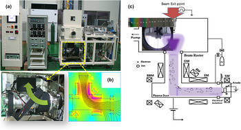
The ta-C coating was deposited on a Si (100) wafer by a single-cathode of FCVA system, as shown in Fig. 1(a). The vacuum arc source with a T-shaped filter is attached to the bottom side of the coating chamber. Before setting-up the FCVA system, a numerical analysis using finite element method magnetics (FEMM) calculated the arc plasma direction at the T-shaped filter and the magnetic field positions shown in Fig. 1(b). A magnetic solenoid is used in the FCVA system to separate charged carbon ions from neutral atoms and macro- or micro-particles.
(a) Single-cathode FCVA coating system, (b) arc plasma beam direction, calculated by numerical analysis (FEMM code), and (c) schematic of the ta-C coating flow during deposition.

Figure 1(c) shows the arc plasma beam moving through the filter from the cathodic arc source. A carbon target of 55 mm diameter and 99.99% purity is mounted on the bottom right side of the chamber. The magnetic coil current is fixed to 5 A. Before the deposition, the Si wafer was cleaned with alcohol and deionized water.
After pumping the chamber to a pressure below 5 × 10⁻³ Pa, the Si wafer was etched for 10 min in arc plasma at 2 × 10⁻¹ Pa. The substrate holder was placed horizontally on a sample carrier with no rotation for high-speed coating at a working pressure below 3–5 × 10⁻² Pa and variable processing parameters. A duct bias of 20 V and a substrate bias varying from 0 to 500 V were applied during the deposition. The Ar gas flowed at a rate of 2 sccm for stable arc plasma generation. The substrate temperature was measured by thermal labeling and a thermocouple during the ta-C coating deposition.
B. Coating analysis
The ta-C coating layer was observed by FE-SEM (Tescan Orsay Holding, Seoul, Korea) and optical microscopy. The residual stress was calculated by the Stoney equation.Reference Gerald Stoney14 The coating stress was obtained by measuring the radius of curvature of the substrate after coating with ta-C. A Raman spectroscope (Horiba Co. Ltd., Seoul, Korea) equipped with an Ar laser with an excitation wave length of 514 nm was used in backscattering geometry to examine the physical structure of the coatings. The incident power on the sample was 2 mW, and the scanning range was 800–1700 cm−1.
The hardness of the ta-C coating was measured using a nanoindenter (CSM Co., Ltd., Suwon, Korea) with a Berkovich tip. The final load and indentation depth were 0.5 mN, and ∼200 nm. The Poisson ratio of the ta-C coatings was assumed to be 0.3. All coating analyses were carried out at 23 °C and 40% humidity.
III. RESULTS AND DISCUSSION
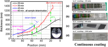
The variation in thickness as a function of the coating time is plotted on the substrate position as shown in Fig. 2. The coating thickness depends on the position of the Si wafer because of the Gaussian distribution of carbon on the Si substrate. An 800 nm thick ta-C coating is obtained from 20 and 30 min of deposition with no delamination. However, interestingly, coatings with thicknesses 1 μm are easily delaminated at a coating time of 30 min. This phenomenon may result from thermal effects; the compressive residual stress for the ta-C coating also contributes to delamination.
To confirm the delamination from thermal effects between the Si wafer and ta-C coating: continuous coating for each time (a) 30 min, (b) 45 min, (c) 60 min, and (d) 300 min.

To confirm the thermal effect, the ta-C coating times were increased to 45, 60, and 300 min. The thickness is saturated at a maximum value of 600 nm for a coating time of 45 min. For film thicknesses exceeding 600 nm at 45 min, the films are delaminated at all positions because of the substrate temperature. At 60 min, delamination occurs across the substrate regardless of thickness. For the 300 min coating process, graphitization occurs in all positions.
Figure 6 shows that, as the coating time is increased, the substrate temperature increases, promoting delamination of the coating. Therefore, to generate a thick ta-C coating, the substrate must be cooled to maintain a suitable temperature. Several reports in the literature discuss about thick ta-C coatings achieved by multilayer films to reduce intrinsic stress.Reference Shan, Wang, Li, Li, Lum and Chen15,Reference Chen, Xu, Du and Liu16 However, this study is focused on ta-C single layers coated on a substrate.
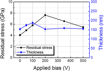
To confirm the direct current (DC) bias effect on the residual stress of the ta-C coating, bias voltages between 0 and 500 V are applied as shown in Fig. 3. During the coating process, the coating and cooling (Ar flowing) times were fixed to 12 and 60 min, respectively. The bias voltage clearly affects the residual stress. The plotted curve shows an increase from 4 to 7.8 GPa between 0 and 200 V and then a decreased from 7.8 to 5 GPa between 200 and 500 V. This can be explained by the thermal effect, in which the acceleration of the positive ion in the arc plasma toward the substrate increases with increasing applied bias. Simultaneously, the substrate temperature is increased. This phenomenon shows that the increase of stress with increased bias results from the decreased coating density.Reference Chhowalla10–Reference Shan, Wang, Li, Li, Lum and Chen15
Thickness and residual stress of the ta-C coating as a function of the substrate bias voltage. To verify the bias effect, the coating and cooling times were fixed to 12 and 60 min, respectively, for all samples.

For the ta-C coating, the residual stress decreases gradually as the high temperature and sp 3 fraction decreases. These changes indicate that the delamination of the ta-C coating is increased by increasing the coating time.
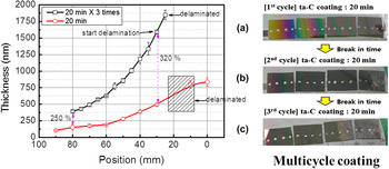
Figure 4 shows the variation in thickness with substrate position for a multicycle growth of a ta-C coating of up to 1 μm in thickness. The coatings are formed in three stages with a total coating time of 60 min. At first, the ta-C coating bias increased to 500 V for 10 min, and then decreased to 0 V for 10 min during the coating process. After each coating stage, a break-in or cooling time of 20 min occurs. The Si substrates were cooled by flowing Ar gas (100 sccm) in the chamber to maintain a constant coating temperature. The second and third stages followed the same procedure. As shown is Figs. 4(b) and 4(c), the ta-C coating thickness of 1.6 μm is successfully increased with increased coating cycles. Furthermore, no delamination occurs from the 50 mm position.
Multicycle coating with constant 20 min coating and break-in (cooling) times, repeated three times.

To confirm the changes in structure from the bias voltage applied during the multicycle coating, Raman spectra analysis was conducted. The Raman spectroscopy analysis results from the different biases 0 and 500 V during the formation of the ta-C coating on the Si wafers are shown in Fig. 5. Raman spectroscopy is a simple nondestructive technique used to characterize the structural changes in carbon-based materials. The thick ta-C coating formed by multicycle coating shows a spectrum in which the G-peak position has shifted from 1580 cm−1 because of the decreased sp 3 content in the thick coating. The D-peak, indicating the degree of disorder in the carbon material, can be seen to increase in intensity for the coating created under 500 V applied bias. These results indicate that the ta-C coating grown under 0 V applied bias has a much greater compressive stress than those grown with applied bias voltages.
Raman spectroscopy analysis of thick ta-C at different bias voltages: 0 V creates hard structure and 500 V creates soft structure. Blue dotted vertical lines are references for G and D peaks.

The ta-C coating formed under 500 V applied bias has a lower compressive stress because of the controlled substrate temperature. Meanwhile, the multicycle ta-C coating formed at a high bias of 500 V has a smaller sp 3 fraction, while the multicycle ta-C film formed at 0 V bias has a larger sp 3 fraction, which is verified by the above-mentioned Raman spectroscopy measurements. The Raman spectra indicate a significant improvement in the stress relaxation of the ta-C coating prepared by the FCVA method. The thick ta-C coating samples had stresses resulting from the combination of the stress values of the hard and soft sublayers within the single-coated layers. The stress properties would therefore likely result from both the total sp 3/sp 2 fraction and the degree of change in the sp 3/sp 2 fraction of the film.Reference Ferrari and Robertson17–Reference Better19
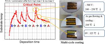
Based on our results, a schematic of the concept for creating thick ta-C coatings is shown in Fig. 6. The coating process is performed by adjusting the substrate bias voltage to high or low levels, then cooling the substrate by flowing Ar gas between periods A and B.
Schematic representation of thick ta-C coating concept: B (high bias) → A (low bias), repeated for multiple cycles to form μm thickness ta-C films. The thermal label was attached to the substrate during ta-C coating.

The substrate temperature and important factor in ta-C growth suppressing the temperature aids the stability of thick ta-C coatings. The substrate temperature is confirmed by the thermal label analyses, as reported in Fig. 6. This demonstrates the change in coating temperatures during the multicycle coating process. This phenomenon indicates that ta-C coatings of thicknesses exceeding 1 μm are successfully deposited on the Si wafer substrate by multicycle coating, in which one cycle consists of 20 min coating and cooling. The sp 3 fraction may relate directly to the residual stress and hardness of the coating.
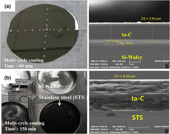
Figure 7 shows FE-SEM images of the cross sections of ta-C coatings on Si and stainless steel substrates with thicknesses of 3.54 and (b) 9.34 μm, respectively. Using multicycle coating process, thick and well-adhered ta-C coatings with reduced stress in ta-C were successfully formed on both substrates. The 9.34 μm thick ta-C coating was formed on the stainless steel substrate over 150 min. The Si wafer was broken without delamination at the interface by crystal fracture because of the high hardness of the coating. The ta-C coating hardness was measured by nanoindentation at the points indicated over 45 GPa.
Optical images and FE-SEM micrographs of thick ta-C coatings on different substrates: (a) 3.54 μm thick ta-C coating on Si wafer, (b) 9.54 μm thick ta-C coating on stainless steel. Si wafer was broken by crystal fracture.

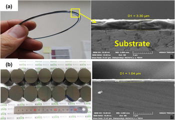
To define the coating performance, we applied thick ta-C coatings to various substrates using the multicycle coating method. Figure 8 shows the thick ta-C coatings on a piston ring, tappet for a gasoline direct-injection (GDI) engine, and cutting tools, formed using FCVA. The ta-C coating surfaces are uniform and smooth with good colors. These ta-C coatings might have high hardness values, ultrahigh load bearing capacities, and low friction coefficients. These properties protect the coating surface, and ensure that automobile components meet the industrial requirements for a wide area of applications. In this study, we only introduced the fabrication concept of thick ta-C coatings for applications. Further investigations on the life-time and failure modes must be conducted in the future.
ta-C coated surfaces with film thicknesses of (a) 3.3 μm on piston ring, (b) 1.2 μm on GDI tappets.

IV. CONCLUSIONS
In this study, we have applied single layers of thick ta-C coatings on various substrates. The ta-C coatings were prepared by FCVA, which enables the investigation of a method for the fabrication of thick ta-C coatings. The following points summarize the information that could be drawn from the present work.
(1) In the case of continuous deposition of a thick ta-C coating, the thickness was limited to 800 nm by the substrate temperature. The thermal effects interact with the residual compressive stresses in the ta-C coating, causing delamination with increase in coating time.
(2) The multicycle ta-C coating process consisted of three steps. The substrate temperature was increased in period B with a high bias of 500 V, then decreased in period A with 0 bias; these periods are followed by a break-in time of 20 min, in which Ar gas is flown at 100 sccm. This process controls the substrate temperature. Therefore, we successfully deposited a 1.6 μm thick ta-C coating on a Si wafer.
(3) Raman spectra analysis revealed that the multicycle ta-C coating formed at a high bias of 500 V had a smaller sp 3 fraction than the film formed at 0 V bias. The structural combinations reduced interfacial stresses and improved the thickness.
(4) A single-layer thick ta-C coating was applied directly on various substrates; a 9.5 μm thick coating was formed on a stainless steel substrate by the multicycle coating method using at FCVA.
ACKNOWLEDGMENTS
This study was supported financially by Fundamental Research Program of the Korea Institute of Materials Science (KIMS), granted financially supported by grant from the Fundamental R&D Program by the Ministry of Science, ICT and Future Planning in Korea. And this paper was originally accepted for and presented at Malaysian International Tribology Conference 2015 (MITC 2015).