Introduction
Over the last three decades, the world of quantum nanomaterials has progressed in leaps and bounds, enabled by great advances in synthesis protocols and measurement tools.Reference Hinterdorfer and Dufrene1 However, control and assembly of nanoscale objects still have a long way to go.Reference Imboden and Bishop2 Currently, applications that exploit nanoscale effects rely on relatively simple materials compositions, without a focus on assembly to higher-level structures. Key examples are binary semiconductor quantum dots for biolabelingReference Michalet, Pinaud, Bentolila, Tsay, Doose, Li, Sundaresan, Wu, Gambhir and Weiss3 and plasmonic metallic nanoparticles for biosensing.Reference Anker, Hall, Lyandres, Shah, Zhao and Van Duyne4 The problems of nanoscale materials being hard to anchor and contact to, and also, that they can have compromised thermal, chemical, and mechanical stability, are all critical issues that need to be addressed.
A paradigm shift in thinking is required to create systems that fully harness low-dimensional phenomena. Spontaneous self-assembly of nanoscale building blocks to higher-level mesoscale architectures is required. Hence, we need to move beyond the reductionist concepts of small sizes and short length scales, toward a constructionist integrated approach for mesoscale practical devices.
The positive features of the mesoscale domain are that quantum effects still come into play since the allowed electronic energy levels are not yet continuous at this scale, but at the same time, the inherent advantages of larger dimensions, notably stability and contactability, can be exploited. An additional opportunity for the mesoscale domain is that as we move up the mesoscale staircase (Figure 1), collective behavior comes into force, giving new degrees of freedom that compete with one another. This leads to coupled electronic interactions (e.g., among magnetic moments, charges, and lattice distortions), resulting in great sensitivity to external stimuli, and ultimately, to high-performance multifunctional systems.
Mesoscale staircase comparing self-assembly of the spiderweb with epitaxial oxide composite devices. (Top staircase, left to right) The spiderweb self-assembles from (1) amino acids to (2) agglomeration of crystalline nanosheets to (3) cross-linking of the sheets by flexible amorphous chains to (4) fibers that form the building blocks of the (5) spiderweb. (Lower staircase, left to right) The parallel mescoscale staircase of the epitaxially directed, self-assembled, oxide composite devices where (1) energetic species in a vapor plume (2) condense onto a single-crystal substrate. (3) Nucleation of crystallites occurs from elemental atoms under high supersaturation, followed by growth of crystallites into phase-separated regions. (4) Devices formed by patterning metallization contacts, (5) followed by integration of these devices and other devices into a chip. (Bottom-right section) Actual composite oxide film structures. (Bottom-left section) Comparison of the surfaces of natural structures (with permission from Reference 7) with an actual composite film surface.

Currently, much of mesoscale science is geared toward chemical and biological applications (e.g., using mesoporous silica),Reference Corma5 but is much less geared toward designing more complex mesoscale electronic devices. In our quest to fill the mesoscale gap, we need to assemble materials in a hierarchical way, from atoms to electronic devices, with materials architectonics (design of materials similar to the way an architect designs a building) guiding the way.Reference Ariga, Yamauchi and Aono6
The staircase of hierarchical assembly from the atomic to the macroscale is what nature does with ease, as in the case of the spiderweb (Figure 1),Reference Keten and Buehler7 so we should be inspired to follow her lead. If we can do this, we will be able to harness collective interactions between entities across the length scales. Of course, nature undergoes dynamic self-assembly and is very fragile and in constant flux. On the other hand, we need to create robust and static products with long-term stability. In the end, an architectonics approach should give much greater functional diversity, efficiency, and interactivity.
In this article, we discuss a relatively new class of mesoscale structure in the form of self-assembled epitaxial composite films. We focus on inorganic functional oxides since this is where most of the work has been done to date. In fact, epitaxial composite films are nonconventional. Most research on novel electronic effects in oxides is focused on planar epitaxial films and artificial superlattice structures made by physical vapor deposition (PVD).Reference Hwang, Iwasa, Kawasaki, Keimer, Nagaosa and Tokura8 However, conventional planar and superlattice structures are limited in terms of their ability to exploit low-dimensional effects. The growth procedures are complex; the substrates on which the films are grown and which dominate the strain states and properties of the films, are limited in composition and lattice type. Some of the substrates required to give very specific lattice constants in the films are also very expensive. Finally, artificially created interfaces formed from dissimilar materials are often imperfect. The main alternative synthesis approach for mesoscale oxides, namely solution chemical routes such as sol-gel or alkali precipitation,Reference Niederberger9 have a different set of limitations (i.e., lower crystallographic perfection, surface degradation, and poor adhesion).
We will illustrate how epitaxial composite oxides can overcome many of the challenges of the aforementioned conventional growth routes. They can deliver very high-quality, size-tunable, substrate-supported, widely strain-tuned, mesoscale structures. In fact, in recent years, novel coupled electronic devices have emerged from these structures, but using only a rather narrow range of known materials. The device aspect was reviewed in a recent issue of MRS Bulletin.Reference Zhang, Ramesh, MacManus-Driscoll and Wang10
To achieve highly sought-after functionalities for future electronic devices (e.g., a room-temperature magnetoelectric, a low-power refrigerant, an energy-efficient harvesting device, etc.), it is likely that composite systems in which two or more materials are coupled together will be required. On the other hand, there is currently little comprehension of which materials systems are compatible with one another in composite films. There is also little understanding about which types of structures (Figure 1) are optimal for a given functionality, about how to design composite structures, or about the new physical effects achievable in them. This article aims to cover what is known, so far, and in doing so, to give better guidance toward the engineering of new functional devices.
Growth of composite epitaxial films
Mesoscopic composite oxide epitaxial films have been grown to date using PVD. Mixed-source ceramic targets containing all of the individual elements to be incorporated in the films are used. Horizontal, vertical, or in-between-alignment phase-separated structures grow by epitaxially directed self-assembly.Reference MacManus-Driscoll11Figure 1 shows key examples of the structures that form. In brief, phase formation in the films depends on both thermodynamic and epitaxial stability. How the phases are distributed depends both on vertical and on horizontal epitaxial stabilization, kinetics, and the ratios of the two phases.Reference Zhao, Li, Lee, Choi, Liang, Zhang, Tang, Wang, Jia, MacManus-Driscoll and Yang12
For epitaxially directed self-assembly, it is desirable that one phase in the film is crystallographically well-matched to the substrate such that it nucleates and grows epitaxially. This phase forms the host matrix. The second phase epitaxially aligns with the matrix phase. We call this phase the epiphyte phase. Depending on surface energy considerations and the relative concentrations of the two components in the film, the epiphyte phase may or may not seed its growth on the substrate. On the other hand, with sufficient kinetics, the epiphyte phase always aligns epitaxially with the matrix. The host and epiphyte can both be chosen to be active phases whose functional properties are of interest. Here, the phases “talk” to one another via strain- or charge-coupling of properties at the interfaces.Reference Zheng, Wang, Lofland, Ma, Mohaddes-Ardabili, Zhao, Salamanca-Riba, Shinde, Ogale, Bai, Viehland, Jia, Schlom, Wuttig, Roytburd and Ramesh13–Reference Liu, Chen, He, Liang, Chen, Chien, Hsieh, Lin, Arenholz, Luo, Chueh, Chen and Chu15 Alternatively, just one of the phases may be functionally active, with the other phase being functionally passive, acting simply to mechanically stabilize or tune the strain state of the active phase.Reference Harrington, Zhai, Denev, Gopalan, Wang, Bi, Redfern, Baek, Bark, Eom, Jia, Vickers and MacManus-Driscoll16
Structures grow either by nucleation and growth (left-two film structures shown at bottom-right section of Figure 1) or by spinodal decomposition (lower-right three film structures shown at bottom-right section of Figure 1). For nucleation and growth, largely immiscible materials need to be chosen, whereas the opposite is true for spinodal ones. We note the similarity of some of the composite epitaxial structures to composite structures found in nature (bottom-left of Figure 1).
In the spinodal case, solid-solution mixing is required at high temperature, followed by one of the phases separating out of the solid solution upon cooling. For example, one can select a perovskite A(B,B′)O3 where B′ substitutes for B at high temperature, but then it separates out of the perovskite phase to leave ABO3 and B′O upon cooling. A and B here represent metal/rare-earth elements. Whether a laterally or vertically ordered spinodal structure or random one forms depends on the crystallographic relation between the decomposing phases, and between the phases and the substrate,Reference Ni, Rao and Khachaturyan17 as well as kinetics. Hence, if the phases are crystallographically similar and sufficient time is allowed for epitaxial growth arrangements, spatially ordered structures can form, although, to date, few ordered spinodal structures have been achieved in electronic materials.Reference Zhang, Yeo, Horibe, Choi, Guha, Croft, Cheong and Mori18,Reference Park, Horibe, Asada, Wielunski, Lee, Bonanno, O’Malley, Sirenko, Kazimirov, Tanimura, Gustafsson and Cheong19 Conversely, if phases are structurally dissimilar or if insufficient time is allowed for separation, large-area disordered structures form.Reference Mecke20
As far as is known, no computational methods have been devised for epitaxial composites to predict which phases will form and in what arrangements they will form, although some modeling has been done for spinodal structure formation.Reference Ni, Rao and Khachaturyan17,Reference Lu, Wang, Gao, Shi, Liu and Wang21 More work in this area would be very useful for predicting structure formation.
Building on the key advantages of composite epitaxial films for creating and exploiting mesoscopic materials, as listed in Figure 1, we now explore their unique properties in more detail.
Mesoscopic host matrix: High phase-purity, high structural quality, lattice uniformity
In composite epitaxial films, highly phase-pure, highly crystalline mesoscopic matrix phases with through-thickness structural uniformity are formed. To illustrate this, we use the example of La1–xSrxMnO3 (LSMO)-based composites with binary second phases of NiO or ZnO, grown on a variety of single-crystal substrates (SrTiO3, LaAlO3, and sapphire). LSMO-based composite structures have been widely explored for providing tunable magnetoresistive and exchange-bias effects.Reference Kang, Wang, MacManus-Driscoll, Li, Jia, Mihut and Betts22–Reference Wu, Cybart, Yi, Parker, Ramesh and Dynes26 In both NiO and ZnO cases, LSMO forms the host matrix since it has better epitaxial matching with the chosen substrates, and the binary oxide forms the epiphyte phase.
First, high phase-purity can be readily achieved in the individual phases in the composites. Figure 2a shows electron micrograph images of an (LSMO)0.5(NiO)0.5 film grown on SrTiO3. This system is being explored for exchange-bias effects.Reference Zhang, Li, Lu, Su, Fan, Khatkhatay, Chen, Jia, Zhang, MacManus-Driscoll and Wang27 The far left image shows a high-resolution planar electron micrograph image of an NiO pillar grown within the LSMO matrix. The film shows a classic nucleation and growth morphology (as shown by the schematic film structure image of Figure 1). Self-assembled NiO columns of ∼3–5 nm diameter were found to be evenly distributed in the LSMO matrix. Energy-dispersive x-ray spectroscopy maps (right images of Figure 2a) showed very distinct phase separation of the NiO and LSMO, indicating minimal intermixing between host and epiphyte phases.
High phase-purity, high structural quality, and lattice uniformity of mesoscopic host matrix in composite films: example of La0.7Sr0.3MnO3 (LSMO). (a) Planar transmission electron micrograph images of (LSMO)0.5(NiO)0.5 film grown on a (001) SrTiO3 single-crystal substrate. Far-left image shows a high-resolution planar electron micrograph image of a single NiO pillar of <5-nm diameter with high epitaxial quality and clean interfaces within the LSMO matrix. Right-hand images show energy-dispersive x-ray spectroscopy maps. Distinct phase separation of NiO and LSMO is observed, indicating minimal intermixing between pillars and matrix. Images adapted with permission from Reference 27. (b) Planar transmission electron microscope (TEM) image of an (LSMO)0.3(ZnO)0.7 film grown on (001) SrTiO3 showing a random (∼5-nm length-scale features) spinodal structure. Image adapted with permission from Reference 29. (c) Planar TEM image of an (LSMO)0.5(ZnO)0.5 film grown on (001) LaAlO3 showing ∼5-nm lateral-width ZnO plates embedded epitaxially within the LSMO matrix. Image adapted with permission from Reference 28. Schematic image below (c) shows crystal orientations of LSMO and ZnO with respect to the SrTiO3 (STO) substrate. Ti atoms in substrate are below the Sr atoms, and the Mn atoms are below the La/Sr atoms and are obscured. (d) Cross-sectional TEM image of an (LSMO)0.5(ZnO)0.5 film grown on (001) LaAlO3 showing clean, epitaxial interfaces between ZnO and LSMO. Adapted with permission from Reference 28. (e) Resistivity normalized by resistivity at 340K (ρ/ρ[340 K]) versus temperature (T) for (LSMO)0.8(ZnO)0.2 film grown on (001) STO compared to plain film of LSMO grown under the same conditions. Plot adapted with permission from Reference 29. The same peak temperature is observed, indicating negligible intermixing of the phases in the film. (f) Lattice parameter LSMO in (LSMO)0.5(ZnO)0.5 films grown on c-plane sapphire versus film thickness. Plot adapted with permission from Reference 28. The LSMO bulk lattice parameter is independent of film thickness owing to vertical strain control from epitaxy with the embedded ZnO plates.
To further demonstrate high phase-purity in composite films, as well as through-thickness structural uniformity, we consider the closely related (LSMO)1x(ZnO)x system.Reference Chen, Weigand, Bi, Zhang, Lu, Dowden, MacManus-Driscoll, Wang and Jia28,Reference Chen, Zhang, Khatkatay, Su, Tsai, Chen, Jia, MacManus-Driscoll and Wang29 Here, depending on growth conditions and the substrate used, either a very fine (∼5-nm length scales for both the LSMO and the ZnO phases) random spinodal structure, as seen in Figure 2b, or a similarly fine (∼20-nm length scale LSMO, with embedded ∼5-nm lateral-width ZnO plates) nucleation and growth structure with very clean epitaxial vertical interfaces (Figure 2c–d) is achieved. For (LSMO)0.8(ZnO)0.2 films, the composite film has bulk-like transport properties with a peak resistivity of ∼340 K, the same as for pure LSMO films grown under the same conditions (see Figure 2e), indicating negligible intermixing of LSMO and ZnO. Proof of the structural uniformity of the composites is that a constant lattice strain is observed through the film thickness, with the bulk LSMO lattice parameter being obtained (Figure 2f), indicating no structural relaxation of the LSMO with thickness. The ZnO epiphyte phase acts as a vertical epitaxial scaffold to fix the LSMO lattice parameters such that they are constant with film thickness, and independent of the substrate, at least above the initial nucleation region (up to ∼10 nm above the substrate). There is no lateral relaxation of strain because the dimensions between the strain-controlling epiphyte pillars are small, (i.e., 20 nm or less).Reference MacManus-Driscoll, Zerrer, Wang, Yang, Yoon, Fouchet, Yu, Blamire and Jia30 The strain state is very different from the case for plain epitaxial films, where strain relaxes gradually with film thickness.Reference Pradhan, Hunter, Williams, Lasley-Hunter, Bah, Mustafa, Rakhimov, Zhang, Sellmyer, Carpenter, Sahu and Huang31
Strong alignment, high structural quality, uniformity of mesoscopic columns
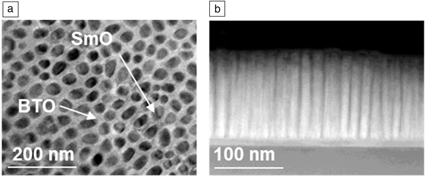
Having shown the high phase-purity, crystallinity, and structural uniformity of the mesoscopic matrix phase in the composite epitaxial films, we now demonstrate that the very fine epiphyte columns have similar properties. We use the example of (SrTiO3)0.5(Sm2O3)0.5 and (BaTiO3)0.5(Sm2O3)0.5 films grown on SrTiO3 (STO). Both of these film compositions show very similar nucleation and growth morphologies, the type shown in the left schematic film image at the bottom of Figure 1. Figure 3a shows a planar transmission electron microscope (TEM) image of a (BaTiO3)0.5(Sm2O3)0.5 film revealing highly aligned, ∼20-nm epiphyte columns of Sm2O3 (SmO) embedded in the BaTiO3 (BTO) host matrix.Reference Harrington, Zhai, Denev, Gopalan, Wang, Bi, Redfern, Baek, Bark, Eom, Jia, Vickers and MacManus-Driscoll16 There is negligible intermixing between phases in this system.Reference Maletic, Popovic and Dojcilovic32 Cross-sectional (scanning)TEM ([S]TEM) images, in Figure 3b shows very strong alignment and clean vertical interfaces in (STO)0.5(SmO)0.5 films. The cross-sectional ([S]TEM) image of Figure 3b shows very strong alignment and clean vertical interfaces in (SrTiO3)0.5(Sm2O3)0.5 film.Reference Lee, Sangle, Lu, Chen, Zhang, Lee, Wang, Jia and MacManus-Driscoll33 Very low tilt values of ∼1° of the pillars in the matrices are observed and the host matrix also does not degrade in alignment or crystallinity with the presence of the pillars. Also, uniform strain is achieved with film thickness.Reference Harrington, Zhai, Denev, Gopalan, Wang, Bi, Redfern, Baek, Bark, Eom, Jia, Vickers and MacManus-Driscoll16 This is very different from plain epitaxial films where, in general, there is a greater distribution of lattice parameters (and microstrain) with film thickness.Reference Harrington, Zhai, Denev, Gopalan, Wang, Bi, Redfern, Baek, Bark, Eom, Jia, Vickers and MacManus-Driscoll16 The reason for the improved film crystallinity with film thickness is that, at first, the substrate plays a lateral epitaxial role, which competes with the vertical epitaxy. However, as the film thickens, only the vertical epitaxy between the two phases in the composite is in operation.
Strong alignment, high structural quality, and high uniformity of mesoscale columns: example of growth of Sm2O3 columns embedded in perovskite titanate matrices. (a) Planar transmission electron microscope (TEM) image of a (BaTiO3)0.5(Sm2O3)0.5 ([BTO]0.5[SmO]0.5) film grown on (001) SrTiO3. ∼20-nm columns of SmO are observed embedded in the BTO matrix. Image adapted with permission from Reference 16. (b) Cross-sectional scanning TEM image of (SrTiO3)0.5(Sm2O3)0.5 ([STO]0.5[SmO]0.5) film grown on STO showing highly parallel columns of SmO (bright) embedded in the perovskite matrix (dark) from Reference 33.
Composite epitaxial stabilization of phases that are structurally mismatched with the substrate
An extension of the benefits of vertical epitaxial growth in the composites, which produces high structural uniformity, crystallinity, and orientation, is synergistic epitaxial stabilization of the epiphyte by the host and of the host by the epiphyte.
An example of the epiphyte stabilizing the host matrix is the LSMO/ZnO system. When plain LSMO is grown on structurally mismatched c-plane sapphire, a single, out-of-plane, (001) orientation of LSMO is obtained only under narrow growth conditions.Reference Chen, Zhang, Jian, Wang, Tsai, Su, Jia and MacManus-Driscoll24 On the other hand, in LSMO/ZnO composites with the ZnO epiphyte and a plate-like scaffold present, a single epitaxial (001) LSMO orientation results over a much wider range of growth conditions.Reference Chen, Zhang, Jian, Wang, Tsai, Su, Jia and MacManus-Driscoll24
An example of the host stabilizing the epiphyte phase is the (Sm-doped CeO2)0.5(SrTiO3)0.5 (SDC/STO) system: Under standard growth conditions of ∼800°C, 20 Pa O2, and for growth of ∼500-nm films on SrTiO3, plain films of the ionic conductor, SDC, grow with mixed orientation and are polycrystalline (Figure 4a). This is because SDC has a fluorite structure that is structurally incompatible with the STO substrate, and therefore, epitaxial growth is hindered. The composite film, on the other hand, produces a single, sharp (001) orientation of SDC (Figure 4b). Because of this, SDC is epitaxially stabilized vertically by the surrounding STO matrix, which grows with (001) aligned on the STO substrate. The highly crystalline, mesoscale ionic columns of SDC have an order of magnitude enhanced ionic conduction compared to plain SDC films.Reference Yang, Lee, Jian, Zhang, Jia, Wang, Noh, Kalinin and MacManus-Driscoll34 Later, we further discuss the advantages of vertically ionically conducting composite systems and mesoscopic ionic conduction effects.
Composite stabilization of epitaxial growth for phases that are structurally mismatched with the substrate. Growth of fluorite Sm-doped CeO2 (SDC) on perovskite SrTiO3 (STO). X-ray diffraction plots of intensity versus 2θ (where 2θ is the angle between x-ray source and detector) for (a) plain Sm-doped CeO2 films grown on (001) SrTiO3, compared to (b) (SDC)0.5(SrTiO3)0.5 (SDC/STO) composite films grown under the same conditions. Polycrystalline films are obtained for the SDC films, whereas a single, sharp, (001) SDC epitaxial orientation is obtained for the composite film. Plots adapted with permission from Reference 34.
Size tuning, property tuning, and spatial ordering
Size tuning of composite films is readily possible by modifying growth parameters (temperature and growth rate), ratio of phases, and composition of the epiphyte phase. We use the example of (BiFeO3)1–x(Fe3O4)x composite epitaxial films grown on (011) SrTiO3. Size tuning of the mesoscopic features was undertaken by varying the phase fractions of the two phases. For x = 0.5, large features in the form of columns of Fe3O4 (∼50 nm) formed in a vertical geometry in the BiFeO3 matrix (Figure 5a). This produced a strong exchange-bias enhancement at room temperature (Figure 5b).Reference Weal, Patnaik, Bi, Wang, Fix, Kursumovic and MacManus-Driscoll35,Reference Choi, Weal, Bi, Wang, Kursumovic, Fix, Blamire and MacManus-Driscoll36 In contrast, for x = 0.1, very fine, ∼5-nm wide, ∼10–20-nm long epitaxial Fe3O4 nanoparticles formed, with a well-defined epitaxial orientation within the BiFeO3 matrix (Figure 5c). This produced a room-temperature exchange bias effect of 40 Oe (3180 A/m) at room temperature (Figure 5d).Reference Weal, Patnaik, Bi, Wang, Fix, Kursumovic and MacManus-Driscoll35,Reference Choi, Weal, Bi, Wang, Kursumovic, Fix, Blamire and MacManus-Driscoll36 The above example demonstrates that the orientation and dimensions of mesoscopic epiphyte second phases are highly tunable by varying the phase fraction and that this leads to entirely different coupled properties.
Size tuning, property tuning, and spatial ordering: example of growth of BiFeO3 (BFO) with embedded spinel ferrites. (a–d) (BiFeO3)1–x(Fe3O4)x composite epitaxial films grown on (011) SrTiO3, showing cross-sectional transmission electron microscope images and magnetization (M) versus field plots for different values of x. (a–b) x = 0.5. Here, strong room-temperature exchange enhancement is observed. (c–d) x = 0.1. Room-temperature exchange-bias is observed (H EB is the exchange-bias field). Room-temperature exchange-bias is observed. Note: 1 Oe = 79.6 A/m. Images and plots adapted with permission from Reference 36. (e) Spatial ordering of ferrimagnetic CoFe2O4 (CFO) pillars in a BiFeO3 matrix grown using alternating deposition of CFO and BFO by pulsed laser deposition and prepatterning of the substrate by focused ion beam. The magnetic spin directions in the pillars can be electrically switched (as shown by up and down spins). Images used with permission from Reference 39.
The reason that it is possible to produce a room-temperature exchange-bias effect in the composite system when it has not been achieved in standard planar, all-oxide epitaxial films is related to the nature of the interfaces formed in the self-assembled composites. In all-oxide planar systems containing BFO and LSMO, exchange-bias was only observed at cryogenic temperatures.Reference Wu, Cybart, Yu, Rossell, Zhang, Ramesh and Dynes37 A low blocking temperature (the temperature at which the exchange-bias field becomes zero) of the exchange-bias (∼100–150 K) was observed, which was postulated to arise from a spin glass (a disordered magnet where magnetic spins are not aligned in a regular pattern) at the domain walls in the BFO at the interface with the LSMO.Reference Xu, Sheng, Xue, Yuan, Wen and Du38
Interfaces in planar epitaxial films often have intermixing at the interfaces, which inevitably degrades the interface properties. Interfaces in self-assembled composites are formed at equilibrium and are not “forced” together by high supersaturation that occurs during thin-film growth. Therefore, the very fact that composites are “natural” because they form by self-assembly necessarily means clean interfaces. Indeed, if any mixing were to take place, it would be over the whole bulk in the form of an entirely new phase and not just the interface.
The disadvantages of the composites is that the library of possible compositions is smaller than for planar lattices, since both thermodynamics and epitaxy limit the range of two phases that can be grown together, whereas in the planar film case, the only limitation is epitaxy. To minimize the disadvantages of a narrower range of possible materials sets in composites, a much broader range of systems should be considered. Fortunately, the combinations of elements in the periodic table at our disposal are almost limitless.
Looking to the future, electrically addressable mesoscale electronic devices are strongly desired, (e.g., multiferroic memory or logic devices) where electric fields can promote reversal of specific mesoscopic magnetic pillars. With this aim in mind, templated, bottom-up growth of ferrimagnetic CoFe2O4 pillars in a BFO matrix were grown using focused ion beam prepatterning of substrates, and this resulted in good spatial ordering of the magnetic pillars, as shown in Figure 5e, as well as the ability to switch the magnetic direction of the pillars using an electric field.Reference Aimon, Kim, Sun and Ross39
There is much potential of these mesoscopic magnetic structures for understanding magnetic frustration in ordered arrays. The composition of the pillars could be adjusted such that the magnetoelastic anisotropy can be controlled or reduced such that magnetostatic interactions become important at sub-100-nm periods. This could allow the design of magnetic quantum cellular automata devices using epitaxial composites.
Another approach for achieving spatial ordering is to use composite film compositions that give highly ordered spinodal structures during growth. However, as previously mentioned, there are limitations on the composition sets that can produce such order.Reference Park, Horibe, Asada, Wielunski, Lee, Bonanno, O’Malley, Sirenko, Kazimirov, Tanimura, Gustafsson and Cheong19 Hence, known spinodal structures could be used to seed order in otherwise spatially random structures that form in most composite systems. Future studies on creating large-area spatial order in inorganic composite films can learn lesssons from templating approaches used for organic diblock copolymer composite films. Here, chemical striping and graphoepitaxy approaches have been successful. Chemical striping involves the lithographic production of a “prepattern” of stripes of alternating chemical composition to guide copolymer formation, and graphoepitaxy creates an artificial surface relief structure on a substrate with a periodic thickness profile to direct and align the copolymer formation, thus giving a micropattern with different lamellar domain orientations mirroring the substrate topography.Reference Stoykovich and Nealey40
Strain tuning and surface stabilization of mesostructures
In strongly correlated functional systems, control of strain is critical to physical properties, since properties are intimately coupled to crystal structure.Reference Takamura, Chopdekar, Arenholz and Suzuki41 In plain epitaxial films, strain is controlled by epitaxy with single-crystal substrates. As already discussed, this is not ideal for two main reasons: first, there are only a limited number of single-crystal substrates available. Second, strain relaxes through the film thickness, and thus, a range of strain states (and therefore, properties) results in a single film.Reference Pradhan, Hunter, Williams, Lasley-Hunter, Bah, Mustafa, Rakhimov, Zhang, Sellmyer, Carpenter, Sahu and Huang31 Hence, in mesoscopic oxides, ways to “dial in” a single, desired level of strain is vital to carefully tuning physical properties and to realizing new properties.
Earlier, we discussed that a uniform strain state is a signature of composite epitaxial films. This is because of vertical epitaxy occurring between the phases in the composite and of the lateral distance between the strain-controlling epiphyte pillars being too small to allow for significant lateral relaxation. It is also important to realize that any lateral relaxation that could occur if the pillar/matrix dimensions are large (i.e., >20 nm) will not depend on film thickness (at least above a thickness where the substrate no longer plays a role), as shown in Figure 2f, and therefore, the composite film properties will not depend on film thickness.
The mechanical properties of the epiphyte pillars are essential for tuning the strain of the host matrix: stiff epiphyte pillars produce high strain states in the host matrix, but, in addition, a large thermal expansion of these stiff pillars induces unusual auxetic-like effects in the matrix. As we show below and demonstrate in Figure 6, newly accessible, thickness-independent physical properties result from these new strain effects in the composites.Reference MacManus-Driscoll, Suwardi, Kursumovic, Bi, Tsai, Wang, Jia and Lee42
Strain tuning and surface stabilization of mesostructures leading to strong property enhancements. (a) (BaTiO3)1–x(Sm2O3)x film grown on SrTiO3 showing unusual auxetic-like strain state, giving a large and positive transverse piezoelectric coefficient, d 31, which is constant with temperature at least up to 250°C. Plot adapted with permission from Reference 43. Left inset shows schematic of composite film structure, and right inset shows transmission electron microscope (TEM) cross section of an actual film. (b) (Ba0.6Sr0.4TiO3)0.25(Sm2O3)0.75 film grown on SrTiO3 showing a high saturation polarization value of ∼120 µC/cm2 in the Ba0.6Sr0.4TiO3 (BSTO) owing to the high out-of-plane tension induced in the BSTO from the stiff SmO matrix. Plot adapted with permission from Reference 42. Inset at top left shows schematic of composite film structure, and right bottom inset shows TEM cross section of an actual film. (c) (SrZrO3)0.5(RE2O3)0.5 (RE = rare-earth) films grown on SrTiO3. The ionic conductivity (σ) of the SrZrO3 (SZO) matrix is proportional to the out-of-plane strain in the SrZrO3, which is tuned using different stiff RE2O3, namely Er2O3, Dy2O3, Gd2O3, Eu2O3, and Sm2O3 pillars. Plot adapted with permission from Reference 47.
We first consider the example of (BaTiO3)1–x(Sm2O3)x ([BTO]1–x[SmO]x) films. Owing to vertical epitaxy of the relatively soft BTO host matrix with the stiffer SmO epiphyte pillars, a large and uniform out-of-plane tension in the BTO of >1% is achieved in relatively thick films (>1 μm). In (BTO)0.50(SmO)0.50 composites, the high out-of-plane strain leads to the ferroelectric transition temperature to increase from 130°C to ∼800°C in the BTO, thus producing a Pb-free, high-temperature ferroelectric material.Reference Harrington, Zhai, Denev, Gopalan, Wang, Bi, Redfern, Baek, Bark, Eom, Jia, Vickers and MacManus-Driscoll16,Reference Kursumovic, Defay, Lee, Tsai, Bi, Wang and MacManus-Driscoll43
Usually, for all values of x ≤ 0.5, BTO forms the matrix and SmO the pillars, and the strain state is auxetic-like. In addition to a large out-of-plane tension of >1%, there is also a large in-plane tension of >1%. The unusual auxetic effect led to a large and positive transverse piezoelectric coefficient, d 31 >200 pm V–1, exceeding the magnitude in lead zirconate titanate (PbZrxTi1–xO3), but being of opposite sign (Figure 6a), and leading to Pb-free microactuator structures that operate at a few hundred °C.Reference Kursumovic, Defay, Lee, Tsai, Bi, Wang and MacManus-Driscoll43 The auxetic-like effect was explained by modeling the strain state in the composite films upon cooling from the growth temperature. It was found that the matrix expands in-plane as a result of the thermal shrinkage of the stiff, epitaxially anchored SmO pillars embedded in the film. The anchoring effect also prevents the tetragonal-to-cubic phase transition from occurring upon heating, thus preserving the ferroelectric state.Reference MacManus-Driscoll, Suwardi, Kursumovic, Bi, Tsai, Wang, Jia and Lee42
In addition to the realization of large and sometimes unusual strain effects as discussed above, a strongly beneficial feature of the composites is stabilization of the surfaces of the mesoscale structures within the films. Consequently, in micrometer-thick epitaxial composites of Ba0.6Sr0.4TiO3 (BSTO) containing only low fractions of BSTO, (i.e., in (BSTO)0.25(SmO)0.75 films) where the SmO forms the matrix and the BSTO forms fine, less than 10 nm, mesopillars, a high level of out-of-plane tension (up to 1.3%) and in-plane compression (also up to 1.3%) is achieved.Reference MacManus-Driscoll, Suwardi, Kursumovic, Bi, Tsai, Wang, Jia and Lee42,Reference Lee, Harrington, Kursumovic, Defay, Wang, Bi, Tsai, Yan, Jia and MacManus-Driscoll44 This gives a very high saturation polarization value of ∼120 µC/cm2 in BSTO, a factor of 3 greater than that found in standard, plain BSTO or BTO films (Figure 6b).Reference MacManus-Driscoll, Suwardi, Kursumovic, Bi, Tsai, Wang, Jia and Lee42
The above mesostructured ferroelectrics formed in composite films show much improved properties compared to freestanding ferroelectric nano/mesopillars of similar or even larger sizes. There, severely degraded properties are obtained,Reference Alexe, Hesse, Schmidt, Senz, Fan, Zacharias and Goesele45 likely because of surface degradation effects (from strain, reconstruction, and chemical degradation).Reference Jing, Duan, Sun, Zhang, Xu, Li, Wang and Yu46 Therefore, the epitaxial composites represent an ideal platform for enabling exploration of the properties of mesoscale structures without being plagued by other deleterious effects associated with modulated, reconstructed, reacted, or degraded surfaces of comparative unsupported low-dimensional structures.
Another example demonstrating that precise strain tuning in epitaxial composites can lead to much improved, tunable physical properties is the (SrZrO3)0.5(RE2O3)0.5 (RE = rare-earth) system (Figure 6c). For films grown on SrTiO3 substrates, the ionic conductivity of the SrZrO3 matrix can be tuned by appropriate choice of the RE in the stiff epiphyte, pillar phase.Reference Lee, Zhang, Khatkatay, Jia, Wang and MacManus-Driscoll47 An increased lattice constant of RE2O3 produces an increase in tensile strain in the SrZrO3 and to a proportionate increase in ionic conductivity in the SrZrO3. An ionic conduction enhancement of over an order of magnitude is achieved (Figure 6c), and strain and crystallinityReference Yang, Lee, Jian, Zhang, Jia, Wang, Noh, Kalinin and MacManus-Driscoll34 both appear to be important factors for enhancing ionic conduction. The crystallinity effect has also been shown in yttria-stabilized zirconia (YSZ) composite films in which perfect YSZ mesopillars are formed.Reference Lee, Zhang, Khatkatay, Wang, Jia and MacManus-Driscoll48
In summary, the three effects of high (and in some cases auxetic-like) strain states, excellent crystallinity, and surface stabilization are key for enabling strongly enhanced physical properties in composite epitaxial films. These three effects cannot be achieved together in any other material form (epitaxial film, bulk, or free nanostructures), and the composites represent a unique platform for unprecedented property tuning of mesoscale materials.
Interface ionics
The importance of strong interplay between the structural, electronic, and magnetic degrees of freedom for realizing novel multifunctional properties are well recognized. A further degree of freedom that has been attracting much attention recently is the ionic degree of freedom. In recent years, the discovery of nanoionic memristive effects (a phenomenon in which the electrical resistance of a material varies according to how much electric current has previously flowed through it) in oxide thin films has sparked many research activities toward a universal device involving terabit memories, logic operators, neuristors (memristors used to create neuron-like behavior), and nanobatteries.
In the most commonly studied memristor devices, standard, single-phase films are used (e.g., TiO2). In these films, switchable, random conducting channels (or filaments) are formed, but a high forming voltage is required to initiate their formation. On the other hand, in composite films with perfectly aligned mesoscopic host matrix + epiphyte columns, straight conducting channels can be pre-engineered into the structures without having to apply a high electric field to create the conducting channels. Hence, in composite epitaxial STO/SmO films, forming-free memristor devices have been obtained (Figure 7a).Reference Lee, Sangle, Lu, Chen, Zhang, Lee, Wang, Jia and MacManus-Driscoll33
Vertical ionic channels in composites compared to ion channels in cell membranes. (a) (SrTiO3)0.5(Sm2O3)0.5 films grown on SrTiO3 (STO) showing forming-free memristor behavior associated with the presence of oxygen vacancies between Sm2O3 columns in a film SrTiO3 matrix (as shown in the electron energy-loss spectroscopy [EELS] plot at the bottom right). Short-range drift of the oxygen vacancies leads to their accumulation at the Pt electrode and to a narrow depletion width, W, a low Schottky barrier height, φB, and a low-resistance state (LRS). The opposite situation holds for the high-resistance state (HRS), as shown in top central plot.Reference Lee, Sangle, Lu, Chen, Zhang, Lee, Wang, Jia and MacManus-Driscoll33 EELS results adapted from Reference 33. (b) Schematic diagram of ion channels in cell membranes that open and close in response to large electric fields generated by large imbalances in the distribution of ions on either side of the cell wall. Note: R, resistance.
A high concentration of mobile oxygen vacancies (in Kröger–Vink notation, Vo¨) was measured at the STO surface along its structurally mismatched interfaces with SmO columns, as shown by the electron energy loss spectroscopy plot in Figure 7a. The movement of Vo¨ toward or away from the top Pt electrodes under the action of a different voltage polarity causes the films to be in either a high-resistance state (HRS) owing to a large Schottky barrier height, or to a low-resistance state (LRS) state, owing to a reduced Schottky barrier height. A resistance variation of two orders of magnitude is achieved and is tunable by varying the laser repetition rate during growth, which produces different-sized mesoscale pillars and densities of conducting channels in the films and also presumably different levels of oxygen nonstoichiometry. Very high uniformity and endurance is also achieved.
Widely varying conduction behavior in oxide films arising from ionic channels activated by applied bias has been observed not only in composite oxide films, but also in plain oxide (Mott insulator) films where open channels for the ready migration of oxygen exist.Reference Jeong, Aetukuri, Graf, Schladt, Samant and Parkin49 Voltage-switchable ionic channels in oxide films with fast-migration channels have similarities to the movement of ions in nerve cell (neuron) membranes in the brain (but with much less complexity). The channels in cell membranes open and close, or gate, in response to large electric fields generated by large imbalances in the distribution of ions on either side of the cell wall (Figure 7b). The rapid movement of electrically charged particles allows brain cells to produce large but brief electrical signals, so they can send messages on a millisecond time scale. There is now a drive to shift conventional computing over to a model that more closely mimics the brain’s own function, capturing the properties of neurons, (i.e., ability to generate a spike or impulse of activity when some threshold is exceeded). The hope is to create much more powerful and efficient computing over conventional silicon-based computing (the brain is more power-efficient than our best silicon-based supercomputers by several orders of magnitude), combining memory and logic operations.Reference Kim, Gaba, Wheeler, Cruz-Albrecht, Hussain, Srinivasa and Lu50 As a completely new concept for future computing, the engineering of ionic channels in mesostructured films, activated by very low biases, is worthy of much deeper exploration.
Summary and outlook
Epitaxial composite films represent a new material form for creating very high-quality self-assembled, coupled mesoscopic structures with unprecedented properties. This article has presented a new architectonics vision for such systems using the example of functional oxides. It has given clues about how to use epitaxially directed self-assembly to move up the hierarchical staircase from atoms to devices. Many novel features of epitaxial composites were discussed, with a strong focus on what these new materials offer, for example, high crystallinity, high structural uniformity with thickness, strong orientation, lack of dependence on the substrate for setting film properties, surface stabilization of mesoscale structures from a few nm to >50 nm, new coupling effects, the formation of phases that would not otherwise be stable, the possibility of spatial ordering, and new ionic interface effects. Also, many examples were given to show that unprecedented new properties can be “dialed-in” to composite films.
To date, composite epitaxial film device properties have focused on a very narrow range of compositions and functionalities. There are many unexplored systems in which magnetism, ionics, ferroelectric, thermal, and mechanical effects, among others, could be coupled and new multifunctional devices could be made. There is a pressing need for such devices to solve current challenges related to low-energy, high-performance computing, energy harvesting, better medical diagnostics, and so on. We also note that one aspect of composites not covered in this review but has interesting potential for the future is the creation of nano- to mesoporous films. Such porous films can be created simply by chemically etching one phase out of the composite and leaving a rigid honeycomb structure, offering potential applications in biosensing, nanofiltration, drug delivery, thermoelectrics, and photocatalysis.
Finally, we note that while epitaxial composite films to date have been grown by pulsed laser deposition, this method has been used for reasons of convenience and ease over necessity. Indeed, other larger-area, low-cost epitaxial growth processes would also be highly applicable to growth of composite films including metal–organic chemical vapor deposition, sputtering, and electron beam/thermal evaporation.
Acknowledgments
J.L.M.-D. gratefully acknowledges support of the European Research Council (ERC-2009-AdG 247276 NOVOX) and the Leverhulme Trust (grant RPG-2015-017). H.W. gratefully acknowledges the support from the US National Science Foundation (DMR-1007969, DMR-1401266, and DMR-0846504). A.S. acknowledges funding from the A* PhD program in Singapore. We acknowledge the assistance of Shin Buhm Lee, Abhijeet Sangle, Eun-Mi Choi, Aiping Chen, Wenrui Zhang, Ping Lu, and Ahmed Kursumovic, for provision of some of the data for, or modification to, the figures.