
I. MOTIVATION
Organic ultra-thin and stretchable devices are expected to have a wide range of applications, e.g., displays, renewable energy, biomedical applications, and in soft robotics. Prototypes have already been successfully demonstrated.Reference Tricoli, Nasiri and De1–Reference Lee, Reuveny, Reeder, Lee, Jin, Liu, Yokota, Sekitani, Isoyama, Abe, Suo and Someya6
However, long term stability and reliability of organic electronic devices are still ongoing challenges and subject to active research. Impressive progress has been reported on improving the material stability, i.e., stabilizing perovskites for photovoltaic (PV) application,Reference Wang, Wright, Elumalai and Uddin7–Reference Hashmi, Tiihonen, Martineau, Ozkan, Vivo, Kaunisto, Ulla, Zakeeruddin and Grätzel9 and improving the stability of organic thin-film transistors (TFTs).Reference Feng, Tang, Zhao, Yang, Hu, Li, Wang and Guo10,Reference Zhao, Yan, Murtaza, Liang, Meng and Huang11 Nevertheless, it is well understood that encapsulation will play a major role when commercializing novel organic electronic devices.Reference Wang, Wright, Elumalai and Uddin7,Reference Leijtens, Bush, Cheacharoen, Beal, Bowring, McGehee, Tress, Schenk, Teuscher, Moser, Rensmo, Hagfeldt, Alam, Gupta, Lou, Ajayan, Bedzyk, Kanatzidis and Mohite8,Reference Gevorgyan, Madsen, Roth, Corazza, Hösel, Søndergaard, Jørgensen and Krebs12,Reference Yu, Yang, Chen, Tao and Liu13
Successful thin film encapsulation (TFE) has been proven commercially viable for organic light emitting diode (OLED) displays on polyimide (PI), which has been commercialized by Samsung in the form of curved displays and soon-to-be-presented in foldable displays.14,Reference Lee15 For the new broader class of devices, high-quality ultra-thin encapsulation must be implemented to achieve appropriate lifetimes for specific applications, meet a variety of mechanical and optical performance requirements, and comply with commercial and cost limitations.
General reviews on barrier technologies and TFE on organic electronics have been published elsewhere.14–Reference Adachi, Hattori, Kaji and Tsujimura17 In this paper, we will discuss and define specific encapsulation requirements for a number of different applications with the objective of highlighting differences and gaps, stimulating research and development in this area.
II. APPLICATIONS FOR ULTRA-THIN AND STRETCHABLE ORGANIC ELECTRONIC DEVICES
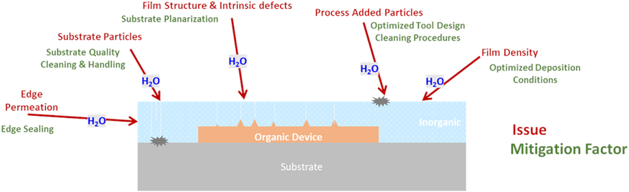
Encapsulation is essential for any type of electronic device to protect it from corrosion of metal lines and contacts, as well as for long-term reliability of functional layers. Organic electronic devices are very sensitive to oxygen and water vapor and suffer from rapid performance degradation when exposed to them. Effective encapsulation with extremely low values of permeation must be realized to deploy organic devices in commercial applications. Single inorganic layers are not effective because particles, film defects, and a limited window in process parameters make them intrinsically defective. Some of the major sources of defects and limitations are qualitatively described by the cartoon reported in Fig. 1. Multilayer (ML) stacks are generally used to circumvent these issues. The fabrication process and application of ML encapsulation stacks are described in the following with respect to specific device requirements.
The 2D schematic shows an organic device (orange) on a substrate (grey) encapsulated by a single inorganic barrier layer (light blue). The red arrows list various issues that can break the protective barrier film and harm the underlying device. In green, different mitigation factors are suggested to improve the encapsulation of the device.

A. OLED display
OLED displays have become a main stream technology in mobile consumer applications in the last few years. Active matrix top emitting OLED, also known as TE-AMOLED, is the technology deployed in mobile (mainly smart phones) applications. Rigid AMOLED displays fabricated on the glass substrate and encapsulated with glass were first launched in mass production by Samsung in 2010 (Samsung Electronics, Suwon, South Korea). The first commercial AMOLED display on plastic foil and TFE with a curved appearance was sold in limited numbers in 2013. Since then, thin AMOLED displays with curved edges have become popular as high-end consumer products and are commercialized by major brands.18
The large-scale mass production deployment of AMOLED displays was made possible by improvements in device lifetime, reliability, performance improvements of the organic materials used in the OLEDs, and further improved by evaporation and masking protocols when depositing the active OLED materials. In addition, the development of effective technologies for flexible substrate fabrication and TFE has played a key role. 10–20 µm thick plastic substrates are fabricated by coating PI on a carrier glass followed by depositing an inorganic layer, usually silicon nitride plasma-enhanced chemical vapor deposition (PECVD), as a barrier to moisture and oxygen permeation. This inorganic layer can be deposited at relatively high temperature because PI is stable up to temperatures in the range of 400 °C. Low-temperature polysilicon (LTPS) TFT arrays are fabricated, followed by an isolation layer, the patterning of the pixel definition layers, and other lithographic structures (e.g., banks), before the evaporation of the OLED stack. Encapsulation of devices is done by ML TFE consisting of a stack of inorganic/organic layers. In the most advanced mobile phone display technology (i.e., Galaxy S8, Samsung, Suwon, South Korea), the touch screen panel is directly fabricated on the display before detaching it from the carrier glass by laser irradiation.
The critical technical requirement in high-end mobile display applications are as follows:
(i) OLEDs are extremely sensitive to moisture and oxygen. OLED failure modes have been extensively discussed in scientific and technical literature. A comprehensive review is provided by Kondarov in Ref. Reference Kondakov, Gaspar and Polikarpov19. Barriers with water vapor transmission rates (WVTRs) lower than 10−6 g/(m2 day) are required to avoid short-term degradation of devices by black spot formation; oxygen transmission rates (OTRs) lower than 10−4 cm3/(m2 day) prevent middle/long-term degradation of light emission efficiency by oxygen.
(ii) In display applications, point defects cannot be tolerated.
(iii) A high number of particles are introduced by the evaporation process of the OLED active layers using shadow masks. To achieve the required resolution for mobile displays (540–580 PPI), fine metal masks are fabricated with special and proprietary technologies and used in strict proximity (∼10 µm) to the display glass. Advanced tools and strict procedures mitigate—but do not avoid—particle contamination on the display glass.
(iv) The inorganic layers have to be processed at low temperature to be compatible with the OLED low temperature constraints (80–100 °C). Low temperature deposition, however, results in poorly conformal, low density, and defect-prone inorganic layers. In addition, during plasma-aided inorganic deposition processes, the plasma energy has to be relatively low to avoid degradation by UV and particles irradiation.
(v) Flexibility requirements limit the thickness of ceramic inorganic layers (max ∼1 µm).
(vi) Encapsulation edges must be as small as possible to minimize the display bezel.
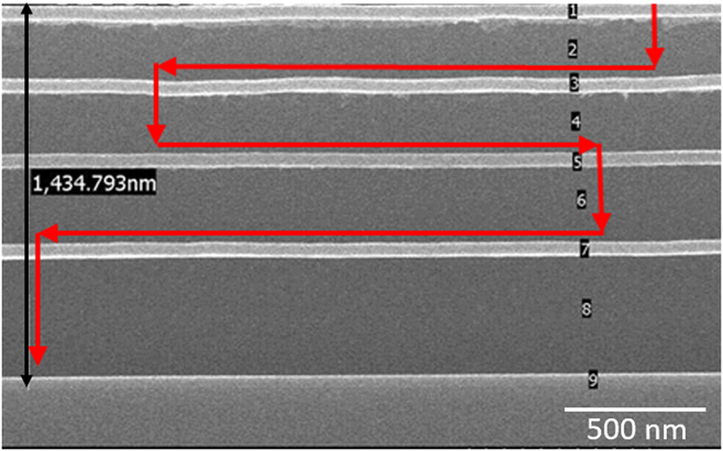
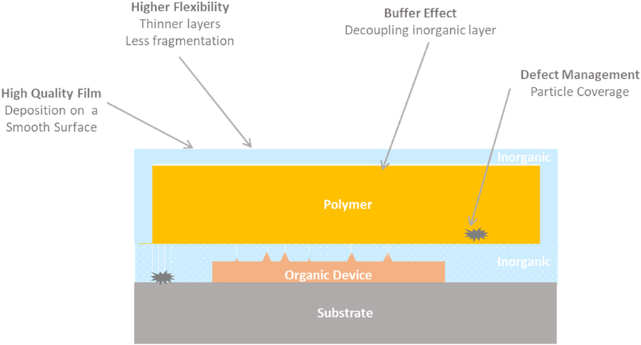
Encapsulation by an inorganic/organic ML stack (Fig. 2) is an effective way to address these challenges. The ML-TFE technology was proposed in the early 2000 by Vitex (San Jose, California)Reference Moro, Krajewski, Rutherford, Philips, Visser, Gross, Bennett, Graff, Kafafi and Lane20,Reference Burrows, Graff, Gross, Martin, Hall, Mast, Bonham, Bennett, Michalski, Weaver, Brown, Fogarty, Sapochak and Kafafi21 and implemented in mass production by Samsung in 2010. Since then, it has become the technology standard for the industry. Redundancy offered by the structure with multiple inorganic layers mitigates the problem of having films with sub-optimal quality and allows the use of thinner films that are more flexible. The organic layers are deposited in liquid form either by polymer vacuum evaporation or by ink-jet printing (IJP).Reference Moro, Krajewski, Rutherford, Philips, Visser, Gross, Bennett, Graff, Kafafi and Lane20,Reference Madigan, Van Slyke and Vronsky22 Blends of monomers cured by UV radiation are currently used. Polymeric films interlayered between inorganic films decouple defects in the inorganic layer preventing the propagation of microstructural faults (i.e., pinholes, grain boundaries, etc.) from one inorganic layer to the next (Fig. 3). Particles introduced by precedent process steps are covered, and a smooth and flat surface is made available for the nucleation of the next inorganic layer. Since fabrication defects are inevitable even on the top inorganic layer, moisture and oxygen may penetrate into the structure. Their diffusion through the ML will occur via a tortuous path created by defects (see red-line in Fig. 2), delaying its arrival to the OLED reactive layers. The mechanism has been described using theoretical modeling,Reference Graff, Williford and Burrows23 and experimentally tested in model structures by X-ray scattering and neutron reflection experiments.Reference Vogt, Lee, Prabhu, DeLongchamp, Lin, Wu and Satija24 Early in the technological development of the ML-TFE technology by Vitex, it had been demonstrated that the proper number of organic/inorganic layers is exclusively defined by the number and size of defects.Reference Chu, Moro and Visser25,Reference Moro, Chu and Hirayama26
The image shows a transmission electron microscopy (TEM) cross section of a ML-TFE stack. The thin light grey layers are the inorganic barrier films and the thicker dark grey layers refer to the polymer films in between. The red arrows indicate a possible path of moisture propagating via defects in the inorganic layer towards the organic device. The diffusion through the ML will occur via a tortuous path, delaying its arrival to the OLED reactive layers.

The 2D schematic provides a simplified picture of state-of-the-art TFE on top of an organic device. The polymeric film interlayered between inorganic films decouples defects in the inorganic layer preventing the propagation of microstructural faults (i.e., pinholes, and grain boundaries) from one inorganic layer to the next.

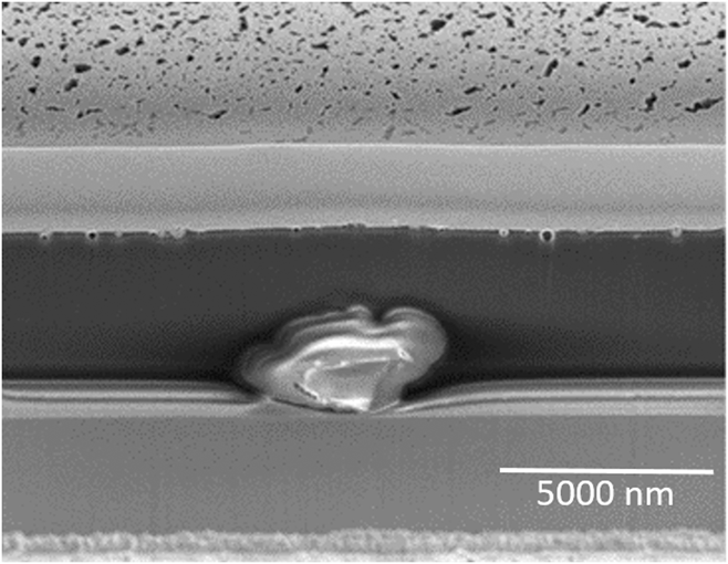
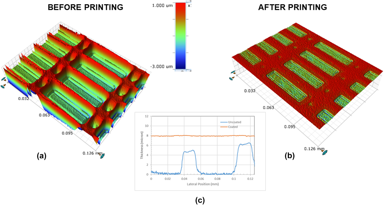
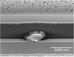
In current commercial devices, the inorganic layer is usually SiNx or SiOxNy deposited by low-temperature (LT) PECVD. The thickness of the layers for the current generation of bendable displays is about 1 µm. Among many materials and deposition techniques, PECVD SiNx has been chosen due to availability of commercially designed tools and the ease of in situ cleaning that allows frequent short cleaning cycles of the deposition chamber, minimizing particle contamination. The polymer layer of 1–4 µm thickness was initially deposited by vacuum evaporation, using shadow masks for patterning. For high volume manufacturing, IJP has been proposedReference Lin, Chu and Rosenblum27 and adopted.Reference Jin, Lee, Kim, An, Straykhilev, Pyo, Kim, Lee, Mo, Kim and Chung28,Reference Hebb29 IJP enables direct and mask-less patterning of the areas to be covered and hence reduces the precursor consumption. Currently, layer thicknesses of 6–10 µm are used. Figure 4 shows the coverage ability of an added particle by an IJP polymer layer.Reference Hebb29 Figure 5(a) shows the morphology of an uncoated display as measured with an optical profilometer. Lithographically defined wells of 1–2 µm in depth are necessary to define and isolate pixels. The integrity of the LT–PECVD SiNx is compromised by the uneven morphology of the display (i.e., microstructural faults at the edges and vertical walls of the wells). The IJP process of the liquid polymer followed by cure creates a perfectly flat surface [see Fig. 5(b)], on which SiNx can nucleate without defects. Today, improved fabrication techniques and procedures have enabled effective ML-TFE with a minimum stack of three layers.
This TEM cross section reveals a particle, introduced by precedent process steps, covered by the polymeric film and resulting in a smooth and flat surface.

(a) shows the morphology of an uncoated display as measured with an optical profilometer. Lithographically defined wells of 1–2 µm in depth are necessary to define and isolate pixels. (b) shows the morphology of a coated display as measured with an optical profilometer. (c) displays the two line profiles of the uncoated display (blue line) and the coated display (orange line). The IJP process of the liquid polymer followed by cure creates a perfectly flat surface.

For TE-AMOLED applications, the optical properties of the TFE stack are very stringent: transparency of the entire stack must be >90–95%, no haze, and neutral color are required. The stack structure and refractive indices of the layers are designed with the help of optical simulations to improve light out-coupling and wide angle view. These properties must be constant over the entire production glass area (>1 m2). Thickness nonuniformity and Mura must be avoided by very advanced engineering and IJP techniques.Reference Madigan, Van Slyke and Vronsky22,Reference Hebb29,Reference Madigan, Hauf, Barkley, Harjee, Vronsky and Van Slyke30 A differentiation point for smart phone displays is the bezel-less design, which is achieved by the implementation of advanced printing algorithms that minimize the edge transition of the TFE layers.
1. OLED displays for wearable applications
Segmented passive matrix OLED (PMOLED) displaysReference Tsujimura31 are more commonly used for wearable applications. PMOLED applications are limited by the size, resolution, and image quality. The main use of PMOLEDs is to display characters and small functional and informative icons for low-cost applications that can tolerate much shorter lifetime. Most PMOLED displays are fabricated on plastic sheets engineered with a barrier and encapsulated with a similar barrier foil laminated on top of the display by applying a low-permeation adhesive, also called “barrier adhesive”. Barrier sheets with a WVTR of 10−5 to 10−6 g/(m2 day) are produced by roll-to-roll deposition by material suppliers. The cost of barrier sheets has recently dropped significantly due to their utilization in mass production of quantum dot (QD) color-enhancing films for QD liquid crystal displays. Despite the lower performance compared to ML-TFE, the barrier foil encapsulation approach is preferred by display makers operating in the wearable market due to low-cost being the dominant parameter over high-performance. The challenge of barrier foils, however, is to obtain perfect edge sealing without side permeation when encapsulating small devices that require a very narrow bezel (<300 µm). Improved encapsulation results are achievable by using the so-called “hybrid encapsulation” scheme, in which the OLED is encapsulated by a combination of an inorganic layer directly deposited on the device followed by a laminated barrier sheet on top.
Cheaper and shorter lifetime PMOLED displays with extreme stretchability have been demonstrated for wearable electronics that can be laminated on the skin for health-monitoring and display information. For these devices, stretchability is obtained by reducing thickness of the display to less than 3 μm with an encapsulation structure done by thin inorganic (e.g., 200 nm SiON)/organic (e.g., 500 nm polymer) MLs.Reference Yokota, Zalar, Kaltenbrunner, Jinno, Matsuhisa, Kitanosako, Tachibana, Yukita, Koizumi and Someya2 In Ref. Reference Yokota, Zalar, Kaltenbrunner, Jinno, Matsuhisa, Kitanosako, Tachibana, Yukita, Koizumi and Someya2, an ultra-flexible reflective pulse oximeter was fabricated by using this technology. The device can be laminated on a finger. The oxygen concentration in the blood is measured and the data are instantly visualized on the body by using an on-skin seven-segment digital display. The lifetime of the device is short (29 h) but adequate for disposable medical applications.
New applications of OLED displays have been presented, each of them offering new challenges for encapsulation. Head-mounted displays have recently attracted attention. Among head-mounted displays, microdisplays (<1″ diagonal) are AMOLED displays fabricated using complementary metal–oxide–semiconductor circuits. Their pixel size is about 3 × 10 µm. The circuit is fabricated by standard IC technology followed by a white OLED deposition by evaporation. The encapsulation typically comprises LT ALD followed by glass encapsulation, using glasses with a photolithographically defined color filter.Reference Ghosh, Donoghue, Khayrullin, Ali, Wacyk, Tice, Vazan, Sziklas, Fellowes and Draper32 Semiconductor-type fabrication processes on Si-wafers, the use of open masks during the deposition of the OLED active layer, and the small size of the displays substantially reduce the number of added particles. Hence, reasonable yields can be achieved using only a single passivation layer. More recently, direct patterning of the RGB emitters has been reported,Reference Ghosh, Donoghue, Khayrullin, Ali, Wacyk, Tice, Vazan, Sziklas, Fellowes and Draper32 and ML-TFE has been used in current devices where the miniaturization of the display size forces elimination of the encapsulation glass and reduces the width available for edge sealing. OLED microdisplays have been proposed and used for military applications, first responders and firefighting application, and in other professional applications (e.g., medical devices, industrial maintenance and service). Consumer applications have been limited to night vision and rifle scopes, while a more general use in glasses has not met large success yet.Reference Levy33
Microdisplays have a high angular resolution (>1.5 arcminute/pixel), but cannot support wide field of view (>90°), required for the new applications of head-mounted displays in virtual and augmented reality (VR/AR). The fabrication technology proposed for these applications is the same as for high-end smartphones. Head-mounted VR/AR displays are larger (∼3.5″ diagonal) and require higher resolution than smartphones. Freeform conformal displays would also be a plus. It has been reported that Samsung demonstrated a high-resolution (1200 PPI) AMOLED panel for VR applications at the 2017 Mobile World Congress.34 This resolution is about two times higher than the resolution currently used in high-end smartphones.
2. OLED displays for automotive applications
Another emerging OLED display application is automotive displays. This application has been made possible by the increased stability of OLED materials to higher temperature (>80 °C) and longer lifetime at relatively high luminance (>600 cd/m2). OLED displays are proposed for use on dashboards where the limited availability of flat surfaces makes OLED displays on flexible substrates and of arbitrary shapes very attractive.Reference Hebb29,Reference Wittmann35 OLED displays fabricated on plastic substrates might also improve the safety in the vehicle since they do not break or shutter under impact. Reduced energy consumption of up to 15% is an additional advantage compared to LCD since only lit OLED pixels consume power. Finally, the intrinsic transparency of OLED materials makes it possible to create head-up displays in the front shield where transparency higher than 70% is often required by regulatory bodies. Encapsulation of automotive displays is mostly done by hybrid or barrier-foil approach.
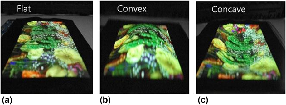
Full freeform involves the evolution from 2D to freeform 3D or conformal displays. While commercial displays have not been produced yet, a stretchable 9.1-inch full-color LTPS AMOLED display with the capability of arbitrary 3D shape transformation has been demonstrated by Samsung (see Fig. 6).Reference Hong, Shin, Kim, Joo, Park, Hwang, Kim, Park, Chu and Kim36 Stretching functionality has been obtained by using the Kirigami-based stretchable technology which makes a thin sheet stretchable by creating holes by cutting.Reference Yokota, Zalar, Kaltenbrunner, Jinno, Matsuhisa, Kitanosako, Tachibana, Yukita, Koizumi and Someya2 The vacuum thermoforming process was then used to give a double curved shape by laminating the stretchable AMOLED panel to a PET foil with an optically clear adhesive. Further encapsulation technology development is needed to translate this prototype display into a commercial product. The displayed prototype might include a lower grade encapsulation using thin ALD layers on the formed 3D display or engineered thin PET foil with ML barrier by thin ALD layer and stretchable polymer. For the commercialization of Kirigami-based stretchable displays, the best approach may be to deposit TFE only in selected areas excluding the sections in which holes are cut.
Photographs of the fabricated 9.1-inch AMOLED display prototype. (a) Flat AMOLED panel before applying the thermoforming process. (b) Convex and (c) Concave-shaped panel produced through the thermoforming process.Reference Hong, Shin, Kim, Joo, Park, Hwang, Kim, Park, Chu and Kim36

B. OLED lighting
OLED lighting has recently attracted interest in high-end automotive applicationsReference Mathas37 and high-end indoor lighting designs,Reference Nguyen38 enabling novel 3D shapes of ultra-thin and flexible light-emitting panels. BMW and Audi have demonstrated OLED rear lights provided by OSRAM OLED GmbH in selected new car models.39
The TFE requirements for OLED lighting are mostly similar to those for OLED displays with respect to oxygen and moisture permeation rates: WVTR lower than 10−6 g/(m2 day) and OTR lower than 10−4 cm3/(m2 day). However, OLEDs for lighting are less sensitive to point defects and have more forgiving specification for edge sealing. Many of the devices are bottom emitting OLEDs; therefore, the barrier foil used as the substrate must be optically transparent, but the encapsulation can be done with opaque foils. The resulting structure has to be ultra-thin and flexible.
The barrier properties are evaluated in accelerated aging tests for >1000 h at 85 °C/85% humidity targeting shelf and operation lifetimes for OLED lighting that are expected to be 5–15 years based on the average ownership of a car and an interior architectural design. In bottom emitting devices, light extraction features can be achieved by the proper choice of the material refractive index and/or inclusion of geometrical structures on the transparent substrates. More advanced and futuristic lighting applications use top emitting devices with encapsulation that has to be transparent in the visible wavelength range and similarly includes light extraction features.
For automotive applications, the OLED light + packaging has to be durable under extreme environmental and temperature conditions. These environmental durability tests are more challenging than those for phone applications. Tests are performed by exposing the devices to H2S and mixed gases making chemical compatibility and inertness of the encapsulation materials an additional requirement.Reference Wittmann35 Temperature durability under extreme usage conditions is evaluated by thermal shock tests—switching the temperature conditions from −40 °C to +85 °C every few seconds. Materials with matching coefficient of thermal expansion must be used to avoid delamination and cracking. Finally, mechanical durability and impact resistance are also tested introducing the extra specification of shock absorbance to the quality of the encapsulation layers.
C. Photovoltaics
In 2017, perovskite solar cells reached certified record efficiencies of 22.7%, exceeding the record efficiencies of various inorganic PV technologies: CIGS (22.6%), CdTe (22.1%), and multicrystalline silicon (22.3%).40 High efficiencies paired with the potential of low-cost device fabrication on flexible substrates have spurred interest in commercialization. To date, the biggest hurdles are device instability and rapid performance degradation.Reference Saliba, Buonassisi, Grätzel, Abate, Tress and Hagfeldt41,Reference Roesch, Faber, Von Hauff, Brown, Lira-Cantu and Hoppe42 Ongoing research is aimed at developing perovskite-inspired absorber materials with improved intrinsic stability.Reference Steinmann, Brandt and Buonassisi43,Reference Brandt, Stevanović, Ginley and Buonassisi44 Improved device lifetime has been demonstrated by inserting an ultra-thin alumina film into a conventional perovskite solar cell structure.Reference Koushik, Verhees, Kuang, Veenstra, Zhang, Verheijen, Creatore and Schropp45 The alumina film directly deposited on top of the perovskite active layer serves as a passivation layer against surface defects, reducing the hysteresis behavior of the device. In addition, the alumina provides some protection against moisture and oxygen entering the perovskite film. To achieve long-term stability of perovskite solar cells, encapsulation will still be needed. Key contributors to perovskite degradation are oxygen, moisture, UV light, and thermal effects. While oxygen only decomposes the perovskite under illumination, moisture causes rapid degradation even in the dark.Reference Wang, Wright, Elumalai and Uddin7
Organic solar cells (based on small molecule or polymer active layers) reveal a similar sensitivity to water and oxygen. Oxidation at the aluminum contacts can result in an oxide layer between the photoactive layer and the contact, hindering the effective charge collection.Reference Gevorgyan, Madsen, Roth, Corazza, Hösel, Søndergaard, Jørgensen and Krebs12 In addition, oxygen and water diffusion into the photoactive layer can trigger chemical and physical degradation mechanisms and hence deteriorate the effectiveness of charge carrier generation and separation in the photoactive layer. In a more specific example, water diffusion can cause aggregation of the fullerene, affecting the metastable morphology of electron donor and acceptor domains.Reference Cheng and Zhan46 Lifetime degradation processes in organic PVs have been studied for decades. A comprehensive overview can be found elsewhere.Reference Gevorgyan, Madsen, Roth, Corazza, Hösel, Søndergaard, Jørgensen and Krebs12,Reference Grossiord, Kroon, Andriessen and Blom47–Reference Neugebauer, Brabec, Hummelen and Sariciftci50
To encapsulate organic solar cells or perovskite-based PV panels, the lamination of barrier foils is likely to be the preferred method. To achieve operation lifetimes competitive with the inorganic counterparts, we estimate that a WVTR of <10−2 g/(m2 day) will be required.Reference Hauch, Schilinsky, Choulis, Rajoelson and Brabec51 The materials used as barriers and substrates must be UV stable to avoid degradation upon exposure to the UV portion of the solar spectrum. Photochemical and photophysical degradation has been observed upon long-term irradiation.Reference Cheng and Zhan46 Planarization layers are to be included in the encapsulation structure to avoid stress-induced cracking of the inorganic barrier layers during the lamination process. Additional characteristics to be considered are electrical isolation, breakdown field, exposure to extreme temperature, and physical impact.
Current PV products on the market offer typical warranties up to a few years for mobile applications and up to 20–25 years for grid installations.Reference Roesch, Faber, Von Hauff, Brown, Lira-Cantu and Hoppe42,Reference Jordan and Kurtz52 Hence, the encapsulation requirements are strongly governed by the application.
Extremely low costReference Powell, Fu, Horowitz, Basore, Woodhouse and Buonassisi53–Reference Powell, Winkler, Goodrich and Buonassisi55 is required for packaging of large-area PV modules in grid installations. To date, the packaging cost of organic PV devices is estimated to be 60% of the entire module cost.Reference Mulligan, Wilson, Bryant, Vaughan, Zhou, Belcher and Dastoor56 Reducing the packaging costs—including the encapsulation—will be a major driving force towards making organic and hybrid organic/inorganic perovskite solar cells competitive for grid installations.Reference Deibel and Dyakonov57
For some high-end PV roof-top installations, ultra-thin and flexible panels integrated in traditional building fabrication components could become very attractive. Barrier encapsulation must be combined with architectural functions to complement environmental durability with the aesthetics of high-end PV system designs.
For mobile PV applications, e.g., military or rescue applications, portable consumer electronics, outdoor and camping, or other off-grid energy requirements, lightweight ultra-thin encapsulation is generally preferred to minimize the weight and size of the product. Many mobile applications might be desired to be flexible, stretchable, or even of arbitrary shapes. In addition, the product needs to be durable and robust. In general, the shelf lifetime of a solar cell integrated in mobile applications needs to be several years. However, much shorter operation lifetimes of months to a few years can be tolerated. Hence, the moisture and oxygen permeation requirements might be less aggressive compared to PV grid installations. An example for a mobile PV application could be an ultra-thin and stretchable solar cell integrated in a tent cover, offering shelter and a source of electricity at the same time.Reference Beckman58 In this application, the encapsulated solar cell has to withstand rough handling (folding and tight packing of the tent cover in storage). When in use, it has to withstand a wide range of weather conditions. Here, lamination of multiple barrier foils engineered with single layer evaporated inorganic films of poor barrier performance is often used for encapsulation to comply with the above requirements and still be cost-effective. With this approach, an effective ML structure is created.
Most high-efficiency hybrid organic/inorganic perovskite solar cells absorb strongly in the visible wavelength range (∼400–800 nm). However, perovskite absorber materials are unstable under UV light.Reference Wang, Wright, Elumalai and Uddin7 State-of-the-art barriers are highly transparent to visible light, but absorb the UV portion of the light. Hence, these could serve well to protect the solar cell from UV light damage.
D. Sensors
Sensors are used across a wide range of applications, e.g., in digital health,Reference Belluck59 biomedical devices,Reference Tricoli, Nasiri and De1,Reference Someya, Bao and Malliaras60,Reference Kaltenbrunner, Sekitani, Reeder, Yokota, Kuribara, Tokuhara, Drack, Schwödiauer, Graz, Bauer-Gogonea, Bauer and Someya61 environmental monitoring,Reference Karim and Zeadally62–Reference Srbinovska, Gavrovski, Dimcev and Krkoleva64 and agriculture and food industry.Reference Ruiz-garcia, Lunadei, Barreiro and Robla65,Reference Khanal, Fulton and Shearer66 To date, however, most of the commercialized sensors are rigid and/or bulky.
Recent progress in the development of flexible organic field effect transistors (OFETs) and photodetectors provides a promising platform to enable ultra-thin and stretchable sensors. While the device performances are approaching those of their inorganic counterparts, OFETs and organic photodetectors are still lacking in device stability and reliability.Reference Zang, Huang, Di and Zhu67,Reference Vuuren, Armin, Pandey, Burn and Meredith68 Further material and device development might yield improved device stability. To commercialize devices with shelf and operational stability and reliability suitable for the application, proper encapsulation will be required. For most sensor applications, long shelf lifetimes are required, meaning that the user has to be able to rely on the functionality of the device even after storing it for several months to years. Operation lifetimes, however, can be much shorter: in biomedical applications, the product might only be used for a few days to weeks. Shelf-life requirement and operational requirement should therefore be decoupled by using proper packaging materials, e.g., metalized ML bags.
While there are no optical transparency requirements for the encapsulation on OFETs, the application of photodetectors requires the encapsulation to be transparent to visible and IR light. One of the key challenges for designing encapsulation for sensors is that the material compatibility requirements strongly depend on the specific application: e.g., for biomedical implants, the encapsulation materials need to be benign for the human body, but themselves resistant to the human body aggressive environment, i.e., sweat, acids, etc. By being chemically inert and available with high purity, silicones and vacuum deposited fluorinated parylene coatings are often used as external encapsulation layers for this type of devices.
In field installation for environmental monitoring, the device packaging has to be very durable in extreme weather and temperature conditions and mechanically reliable. For example, for strain sensors to be used as engineering and architectural monitoring of building and structures, the encapsulation is required to be highly stretchable and to be consistent and reliable. Polymeric coating must be used. For some types of sensors, permeation and diffusion of specific compounds through the encapsulation is required for functioning. Semiporous media must be included in the encapsulation to allow selective permeation. Many of the proposed applications of organic sensors, some in the form of fiber or yarn, involve integration with textile products used in sport or medicine. In this case, breathability (as special case of selective permeation), comfort, and—in some cases—resistance to repeated washing are necessary for successful commercialization. Most of the currently deployed solutions sandwich the sensor between engineered plastic sheets and then laminate it on the textile in a specific position. Better solutions including encapsulation by directly coating on the sensor-fiber/yarn are required.
III. TESTING FOR DEVICE DURABILITY AND LIFETIME
Considering the wide variety of applications for ultra-thin and stretchable organic electronic devices, it becomes apparent that each application implies different requirements for device durability and operation lifetime. We expect the shelf lifetime to be on par with the operation lifetime for most products. For low-cost mobile PV and sensor applications, however, the required storage time might be significantly longer than the operation time.
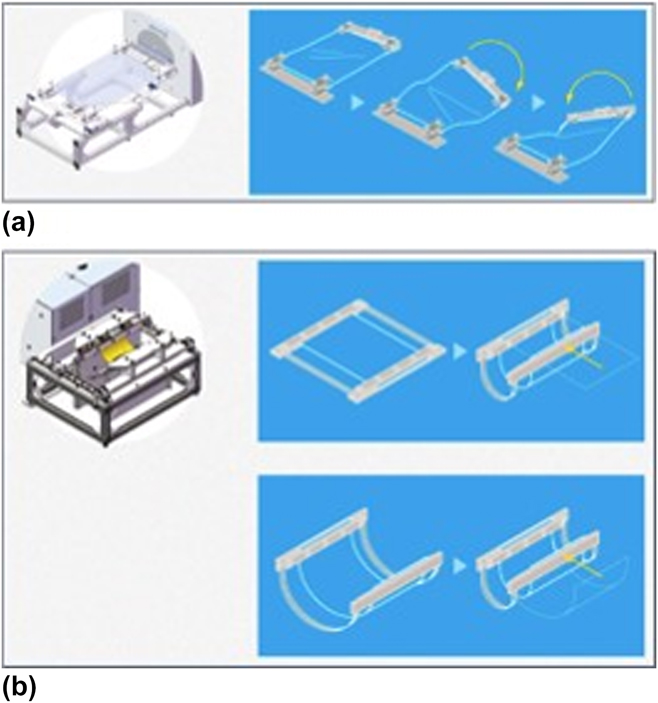
Endurance tests (i.e., stretching, bending, and twisting) are performed to evaluate the mechanical stability and device durability. Figure 7 shows two exemplary R&D systems designed for twisting and bending tests on, e.g., a film or a device. The twisting angle and the bending radius can be defined and varied. The user further defines the numbers of testing cycles. After the testing is completed, the surface of the sample is inspected—visually or under an optical microscope—for evidence of cracks or surface irregularities.
Desktop model endurance testing machine for (a) torsion test for planar object and (b) tension-free u-shape folding test.77

We performed bending tests on SiNx barrier films on 125 μm PEN substrates on a Yuasa flex tool (Yuasa System Co., Ltd., Tokyo, Japan) in tension and compression. In tension, cracks became visible after 50 k cycles at a 9 mm bending radius corresponding to the strain εmax < 0.23%. In compression, we tested SiNx films of three different thicknesses (100, 250, and 500 nm) and at four different bending radii (5.0, 4.2, 3.8, and 3.0 mm) corresponding to 0.05% < εmax < 0.11%. We observed that the thicker SiNx films were bendable at a smaller bending radius before cracks appeared, which is in agreement with thin film mechanics consideration.Reference Ruiz-garcia, Lunadei, Barreiro and Robla65
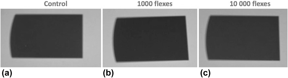
Cracking can be avoided and barrier performance can be maintained by correct design of the ML stack and placing the brittle layers at the neutral plane of the final structure. As an example, Fig. 8 shows the results of testing the flexibility of a single inorganic layer barrier structure on PEN by Ca-test.Reference Nisato, Kuilder, Bouten, Moro, Philips and Rutherford70 The barrier film was laminated after deposition on a thin Ca film to be used as the moisture permeation detection sensor (upon reaction with moisture, transparent Ca-oxide is formed). After 10 k cycles at a 10 mm bending radius and aging for 1000 h at 85 °C/85% RH, the metallic Ca-film is still perfectly reflective. The incorporation of thinner inorganic barrier films (e.g., using ALD) is being explored to increase the critical strain towards enabling more flexible TFE. Since even for thin ALD layers, εmax is <1.0–1.1%, stretchable TFE may be envisioned by the deposition of TFE structures on buckled surfaces of thin substrates or by deposition on selected areas as described above in Sec. II.A.2. However, the development of stretchable encapsulation structures guaranteeing long lifetime of stretchable devices remains one of the most exciting challenges in the TFE technology.
The samples comprise an inorganic barrier film laminated on a thin Ca film on a flexible PEN substrate. All three samples were aged at 85 °C/85% RH for 1000 h. The images show (a) the control sample without flexing, (b) the sample was flexed 1000 times before aging, and (c) the sample was flexed 10 k times before aging. The Ca film is used as a moisture permeation detection sensor after aging (upon reaction with moisture transparent Ca-oxide is formed). The Ca film remains unchanged and perfectly reflective on all three samples, indicating no cracking of the inorganic barrier film even after 10 k flexing cycles at a bending radius of 10 mm.

Accelerated aging tests at 60 °C/90% humidity and 85 °C/85% humidity are the industry standards—established by industrial bodies for certification of consumer electronics—for evaluating the encapsulation performance against water and oxygen.
In accelerated aging testing, it is assumed that an Arrhenius relationship with activation energy, E a, is valid for permeation at different temperatures. This dependence is used in extrapolating permeation at different working conditions. Activation energies can be found experimentally by measuring permeation at different temperatures. In this relationship, the dominant contribution to E a is the dependence of the water vapor saturation concentration at a given temperature. The order of magnitude of the acceleration factors is generally agreed upon despite differences in specific values measured by different methods. It is generally accepted that 1000 h at 60 °C/90% RH is equivalent to a lifetime of few years (<5 years) at 20 °C/50% RH, and 1000 h at 85 °C/85% RH is required for applications with lifetimes longer than 10 years. Caution must be paid in the choice of encapsulation because accelerated testing implies that materials and structures are exposed to higher temperatures than operational ones and must overcome failure modes that are not necessarily seen in the actual device life.
There are a variety of tests adapted in industry to test the device stability and reliability under extreme operational conditions. To study the impact of extreme temperatures, thermal shock testing is used. The devices are automatically moved between two chambers held at different temperatures. Typical testing conditions are 100–500 cycles between −40 °C and +85 °C with switch every 10–30 s. To evaluate the impact of sun exposure on electronic devices, UV irradiation by Xe lamps simulating solar illumination is used in combination with high temperature. Tests under exposure of corrosive gases or liquids (e.g., salted water) are utilized to evaluate durability in aggressive environments.
IV. CONCLUSION
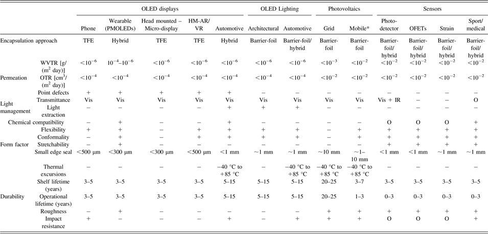
In this paper, we have discussed the stability and reliability requirements for a number of organic electronic devices and their applications. It is apparent that encapsulation is needed. The encapsulation approach, however, varies and depends strongly on the specific application. Table I summarizes the stability and reliability requirements as well as the encapsulation approaches for various applications addressed in Section II of this paper. For some mobile applications (i.e., outdoor PV, sensors, and wearable medical devices) that might have significantly longer shelf lifetime requirements than operational lifetimes, it is important to decouple device encapsulation from proper packaging during storage. Encapsulation for flexible electronic devices has already been demonstrated and commercialized. Examples include flexible OLED displays that can be found in smartphones and wearable devices, and flexible solar cells that are used for mobile off-grid energy generation.
Summary of stability and reliability requirements for various applications of ultra-thin and stretchable organic electronic devices, including OLED displays, OLED lighting, PVs, and sensors. The “+” and “−” symbols indicate the high and low significance of each requirement. The “O” symbol signifies that the requirement strongly depends on the specific application and cannot be generalized. In addition, we state the encapsulation approach for each application. Note that the PV mobile* category specifically refers to military, rescue, and outdoor sport applications.

Future applications of ultra-thin and stretchable organic electronic devices, however, will require additional materials research and an advanced TFE stack design to develop adequate encapsulation. Similarly, research is needed for semiporous barriers to encapsulate chemical sensors based on compound recognition. The barrier has to protect the underlying device against, e.g., moisture and oxygen, but at the same time allow diffusion of other gases or liquids that it needs to be detectable by the device.
Historically, academic research has primarily focused on the performance development of organic electronic devices, with little attention to device stability and reliability requirements.Reference de Goede, Bouten, Médico, Leterrier, Månson and Nisato69,Reference Kim, Singh, Wang, Fuentes-Hernandez, Kippelen and Graham71–Reference Cai, Miller, Tappan and Dauskardt76 By encouraging academic research on encapsulation for ultra-thin and stretchable organic electronic devices, we believe that the gap between device prototyping and product realization can be bridged.
ACKNOWLEDGMENT
The authors acknowledge their colleagues at Kateeva Inc. with special thanks to Brian E. Lassiter, Teresa Ramos, June Zhang, Chris Hauf, and Conor Madigan for their support and fruitful scientific discussions.