I. INTRODUCTION
Technological upgradation is possible by manufacturing nanodevices with the miniaturization mechanism for semiconducting materials. However, during the miniaturization process, the materials should exhibit functional properties and also mechanically robust to sustain higher resistance to damage. In recent decades, versatility and diverse properties as well as facile synthesis of zinc oxide (ZnO) nanostructures are gaining significant technological importance among all compound semiconductors. Its direct band gap of 3.37 eV at room temperature, high electromechanical coupling constant, high exciton binding energy of ∼60 meV, and excellent optoelectrical properties make it suitable candidate for nanodevice applications.Reference Özgür, Alivov, Liu, Teke, Reshchikov, Doğan, Avrutin, Cho and Morkoc1 Nanostructured ZnO can be synthesized using several physical and chemical techniques along with the microstructure manipulations.Reference Klingshirn, Waag, Hoffmann and Geurts2 Doping in ZnO also enhances various electrical and optical properties of interest.Reference Norton, Heo, Ivill, Ip, Pearton, Chisholm and Steiner3 Introducing an optimum percentage of impurity in ZnO alters the defect structure, thereby influencing its physical properties. There are numerous methods to dope rare earth elements in ZnO, which can enhance optical, magnetic, and piezoelectric properties.Reference Norton, Heo, Ivill, Ip, Pearton, Chisholm and Steiner3,Reference Daksh and Agrawal4 Recently, numerous physical and chemical techniques have been established to prepare ZnO films such as sputtering,Reference Bhardwaj, Chowdhury and Jayaganthan5 spray coating,Reference Marouf, Beniaiche, Kardarian, Mendes, Sanchez-Sobrado, Águas, Fortunato and Martins6 pulsed laser deposition,Reference Perrière, Jedrecy, Millon, Cachoncinlle, Talbi, Demange, Guilloux-Viry and Nistor7 chemical vapor deposition,Reference Lin, Chen, Lin, Wang, Chen, Chen, Wen, Chou and Chang8 atomic layer deposition,Reference Hsieh, Wadekar, Liu, Lee, Chang, Tu, You, Chen, Huang and Ho9 sol–gel spin coating,Reference Jacob, Balakrishnan, Meher, Shambavi and Alex10 etc. Among them, sputtering is preferable due to its relatively high deposition rate, low substrate temperature, high film thickness uniformity, and good controllability on morphology with high repeatability.Reference Kelly and Arnell11 Thickness, crystalline orientation, and microstructure of thin films can be manipulated by controlling the sputtering parameters such as distance between substrate and target, sputtering power, gas flow rate, sputtering deposition pressure, deposition time, and substrate temperature. Reactive gases such as nitrogen, oxygen, etc. inserted into the sputtering chamber to deposit compound thin films. The deposition rate is also influenced due to the difference in the masses of reactive gases and argon.Reference Kelly and Arnell11
Rare earth ions incorporated in ZnO have shown the enhancement of several properties including photocatalytic activity, luminescence properties, gas sensing, magnetic properties, optical properties, etc.Reference Daksh and Agrawal4,Reference Dakhel12–Reference Zheng, Song, Jiang and Lian14 Moreover, ZnO–Bi2O3 or addition of MnO2, Bi2O3, and Co3O4-based ceramics are used in electronic devices as varistors due to their nonlinear current–voltage characteristics, energy handling capabilities,Reference Xu, He, Yu, Tong, Qi, Sun, Yang, Xu, Yuan and Ma15 and pyroelectric sensors.Reference Hsiao and Yu16 Pr6O11-based ZnO varistors provide substitution for Bi2O3-based ZnO varistorsReference Senda and Bradt17 and thin films of Pr6O11-doped ZnO can also be used as varistor applications.Reference Wang, Peng, Wang, Wang and Fu18 Even a small amount of Pr content could improve optoelectrical performance,Reference Dakhel12,Reference Li, Meng, Liu, Zhang and Cheng19 photocatalytic activity,Reference Divya and Pradyumnan20 and photoelectric and luminescent properties of ZnO thin films.Reference Li, Meng, Liu, Zhang and Cheng19,Reference Balestrieri, Gallart, Ziegler, Bazylewski, Ferblantier, Schmerber, Chang, Gilliot, Muller and Slaoui21 In addition, Pr-doped ZnO thin films were studied for optical and electrical properties. The mechanical properties of bulk materials can be studied using conventional Vickers hardness testing. However, for nanostructured materials, depth-sensitive nanoindentation is a powerful technique to study the deformation mechanism at small-scale applications. The nanoindentation technique can provide local information of mechanical behavior of the coated system in a small region without detaching it from the substrate. During nanoindentation, load-indentation depth curve is generated from which hardness and Young’ modulus properties can be evaluated. Nanoscratch on the coated system in the load ramp-up mode provides the critical load for coating failure or delamination.Reference Bull22 In addition, progressively increasing load provides the film damage mechanics throughout the whole range of normal and lateral forces as well as viscoelastic properties, phase transformation, friction, and wear properties.Reference Shi, Zhao, Huang, Wan, Ma, Geng and Ren23 The nanoscratch test can also probe the cracking, chipping, and buckling events observed during the onset of failure in thin films.Reference Fu, Chang, Yang, Sheppard, Wang, Maandal and Ye24 The bulk ZnO with a hardness value of 5.0 ± 0.1 GPa, at penetration depth ∼300 nm has been reported,Reference Kucheyev, Bradby, Williams, Jagadish and Swain25 which is prone to damage. However, there is considerable difference in hardness depending upon the morphologies of the ZnO nanostructure.Reference Kang, Kim, Jeon, Kim, Jang, Han and Kim26,Reference Tiwary, Kushagra, Kandpal and Rao27 Mechanical properties of ZnO thin films are influenced by crystalline orientation,Reference Juday, Silva, Huang, Caldas, Prioli and Ponce28 deposition parameters,Reference Yuan, Wang, Tan, Wang, Chen and Ding29 grain size effect,Reference Yen, Jian, Chen, Lin, Lee, Ke, Liao, Yang, Wang and Lai30 different indentation loads,Reference Fang, Chang and Lin31 and creep behaviorReference Fang, Chang and Lin31 as well as doping element.Reference Wang, Lin, Jian, Juang, Jang and Tseng32–Reference Yun, Yue, Peng-Fei, Hong-Yu and Shou-Yu35 The evaluation of mechanical properties of thin films depends upon the type of indenter such as Berkovich, spherical or Knoop, and underlying substrates.Reference Huang and Chang36 The deformation mechanism by indentation loading is primarily depends on slip events through basal and pyramidal planes in ZnO.Reference Bradby, Kucheyev, Williams, Jagadish, Swain, Munroe and Phillips37 The literature on mechanical properties of rare earth-doped ZnO thin films is limited. Hence, the present work is focused to study the hardness, Young’s modulus, and scratch behavior of Pr-doped ZnO thin films using the nanoindentation technique.
II. EXPERIMENTAL DETAILS
A. Growth of Pr-doped ZnO thin films
Pr (praseodymium)-doped ZnO thin films (ZnO:Pr) were deposited using DC sputtering simultaneously on the corning glass substrate and fused quartz substrate at different sputtering pressures, e.g., 5 and 10 mtorr using ZnO:Pr6O11 (97:3 at.%) target. Corning glass and fused quartz substrates were ultrasonically cleaned in distilled water, acetone and dried before putting into the sputtering chamber. Afterward, the sputtering chamber is prepared to evacuate residual gases present in the chamber and a vacuum is established up to a base pressure of 4.3 × 10⁻⁶ torr. The deposition is carried out at Ar:O2 gas inserted to the chamber and flow regulated at 20:5 sccm. Sputtering deposition pressure during deposition of thin films was varied at 5 and 10 mtorr, while maintaining other sputtering parameters, e.g., substrate temperature at 200 °C, sputtering power 50 W, target–substrate distance 4.5 cm, and deposition time 20 min constant for both substrates. The thickness of the glass substrate and fused quartz was 1.33 mm and 1.51 mm, respectively. In addition, presputtering was performed to get clean target free from surface contamination.
B. Structural and roughness analysis
The crystalline structure of ZnO:Pr thin films were examined using characteristic Cu Kα with wave length λ on a X-ray diffractometer (XRD diffractometer Bruker AXS, D8 Advance, Bruker Corp., Karlsruhe, Germany). The angular spectrum ‘2θ’ varies as 25–70°, and the crystallite size ‘D’ was calculated by using Debye Scherrer’s equation as given in Eq. (1),Reference Sagalowicz and Fox38,Reference Cullity and Weymouth39 where β, ‘k’, and θ represent peak width (full width at half maximum), shape factor, and Braggs angle, respectively. Shape factor ‘k’ was taken 0.9, and wave length ‘λ’ of Cu Kα radiation is used 1.54 Å in Eq. (1).
 $$D = {{k\lambda } \over {\beta \cos \theta }}\quad .$$
However, the presence of lattice strain during the growth of ZnO:Pr thin films in XRD peak can be quantified using Stokes Wilson equation by the XRD peak profile in Eq. (2).Reference Stokes and Wilson40
 $$\varepsilon = {\beta \over {4\tan \theta }}\quad .$$
Atomic force microscopy (AFM; NTEGRA, NT-MDT Spectrum Instruments, Moscow, Russia) operated in the semicontact mode using a pyramidal tip coated with silicon nitride (Si3N4) used to measure surface roughness parameters. The RMS roughness varies with peak to valley height difference within a scanned area. AFM images were analyzed using software Nova 1.0.26, NT-MDT, Moscow, Russia. X-ray photoelectron spectroscopy (XPS) of the films was performed to get the stoichiometry and chemical state of Pr (praseodymium) and host matrix ZnO was analyzed by using an Omicron ESCA (Scienta Omicron GmbH, Taunusstein, Germany) instrument. The instrument FE-SEM/EDS (Ultra Plus, Carl Zeiss, Oberkochen, Germany) is used for morphology, cross-sectional thickness, and elemental scanning.
C. Nanomechanical analysis
Mechanical properties of thin films depend on growth, crystal structure and affected by doping, strain, grain size, substrate effect, etc.Reference Kolodziejczyk, Szymanski, Batory and Jedrzejczak41 A nanoindentor with a Berkovich tip of radius 100 nm (Hysitron TI-950, Minneapolis, Minnesota) was used in the present work. The Berkovich tip considered as sharp tip having a three-sided geometry, which terminates at the end. However, a transition depth for the Berkovich tip beyond that tip act as sharp indenter is 0.09R, where R is the tip radius, i.e., 100 nm. Hence, beyond 9 nm, the indenter could be treated as sharp to get elastic–plastic properties.Reference Gouldstone, Koh, Zeng, Giannakopoulos and Suresh42 Area function calibration of the tip on aluminum has certain limitations and cannot provide reliable area function calibration less than 500 nm. For small depth, area function calibrations were performed on fused quartz same as in the present work, which can be applied over the range of 20–7000 nm to ensure reliable results.Reference Tsui, Oliver and Pharr43 The load (µN)–displacement (nm) provides depth sensing mechanical responses of spatial location on thin films during loading/unloading segments.Reference Oliver and Pharr44 However, the consumed total energy pertained to the whole process is correlated with the bound area by curve load (P max)–displacement (h max), while elastic deformation energy is indicated by the area under unloading curve.Reference Zhang45 Nanoindentation is performed in continuous operating normal load up to maximum load (500 µN) in a load-controlled mode at loading rate 62.5 µN/s. The maximum load is chosen by optimizing the average penetration of indenter. Several other factors influence accurate measurement in nanoindentation such as machine compliance, thermal drift, and indentation size effect.Reference Fischer-Cripps46 The relative mechanical performance is presented here as a function of different sputtering pressures.
The scratch testing of the ZnO:Pr thin films is performed using the Berkovich tip to get frictional forces and coefficient of friction. The critical load of film failure, i.e., normal load at which a discontinuity in lateral force is observed indicating film material peel-off, could be observed by the scratch ramp-up mode.Reference Tian and Liu47 However, failure events could be related to several mechanisms related to film cohesive strength, film-substrate adhesive strength, and also influenced by material brittle-ductile nature, which overall affect the critical load. The scratch is performed using ramp-up normal load of 0–3000 µN with the normal loading rate applied 100 µN/s for 30 s. The scratch length was 10 µm (time; 8–38 s) in each test. Several scratch tests were performed to access critical load and film failure of the films.
III. RESULTS AND DISCUSSION
A. X-ray diffraction analysis of ZnO:Pr thin films
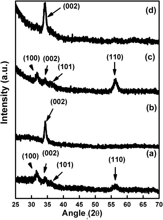
Pr-doped ZnO thin films having thicknesses of 220, 240, 270, and 310 nm were deposited on a fused quartz/corning glass substrate and their XRD scan (θ–2θ) is given in Fig. 1. It is observed at 10 mtorr pressure, the optimized deposition rate is invoked to grow ZnO:Pr thin films preferentially in c-axis crystalline orientation with better crystallinity. Films grown at 5 mtorr pressure appeared with several crystal planes, e.g., (100), (002), (101), and (110), observed as polycrystalline accompanied amorphous in nature. However, the crystal structure of thin films deposited on both substrates is found to be standard wurtzite hexagonal crystal structure ZnO (Ref-JCPDS Card-891397).Reference He48 No separate XRD peak corresponding to Pr element or any impurities/residues is appeared within the detection limit of XRD, as shown in Fig. 1. This could be related to low at.% of Pr in ZnO thin films as mentioned in Table I, as well as Pr ions are dispersed in the ZnO lattice. Since rare earth elements having a quite dissimilar ionic radii compared to the cation (Zn ion), so incorporation of Pr ions (Pr+3/Pr+4) of radius 1.09 Å/0.92 Å into Zn2+ of radius 0.74 Å within the host may cause the replacement of Zn cations or Pr making a separate phase with oxygen change the bonding characteristics within the lattice.Reference Wang, Peng, Wang, Wang and Fu18,Reference He48 The crystallinity and microstructure heavily depend on the Pr content in the film, even a small amount of Pr ions in ZnO affects crystallite size and formation of polycrystalline aggregates as well as the dislocation mechanism along with the defect state, which can generate as tailing effect in overall band gap reported.Reference Divya and Pradyumnan20 The different sputtering pressure influencing mean free path could lead to variation in collision frequency, deposition rate, and the striking energy of ad-atoms, which affects the nucleation and growth conditions.Reference Dave, Dubey, Gupta and Chandra49 The similar response observed and marked a difference in crystallinity and crystal orientation in XRD spectra as shown in Fig. 1. Self-heating feature in sputtering offers the crystalline films even at low temperature and the crystal orientations could follow surface energy minimization.Reference Bao, Gu and Kuang50,Reference Kim, Yim, Cho, Leem, Lee, Kim, Kim and Son51 The growth of films observed with single XRD diffraction peak on the amorphous substrate, which is without long range crystalline order has special significance as can be seen from Fig. 1 for the films deposited at 10 mtorr pressure.
XRD pattern of ZnO:Pr thin films deposited at (a) 5 mtorr @ glass substrate, (b) 10 mtorr @ glass substrate, (c) 5 mtorr @ fused-quartz substrate, and (d) 10 mtorr @ fused-quartz substrate.

Properties of ZnO:Pr thin films.

The peak position, full width half maximum is taken from the (002) XRD peak to calculate the crystallite size using Scherrer’s formula in Eq. (1), and crystallite sizes varied from 11.1 to 15.0 nm. The peak position in 2θ, crystallite size, lattice strain, and crystal d-spacing are provided in Table I. There are slight variations in the crystallite size depending upon the sputtering deposition pressure variation and substrate effect.
B. XPS and morphological analysis of ZnO:Pr thin films
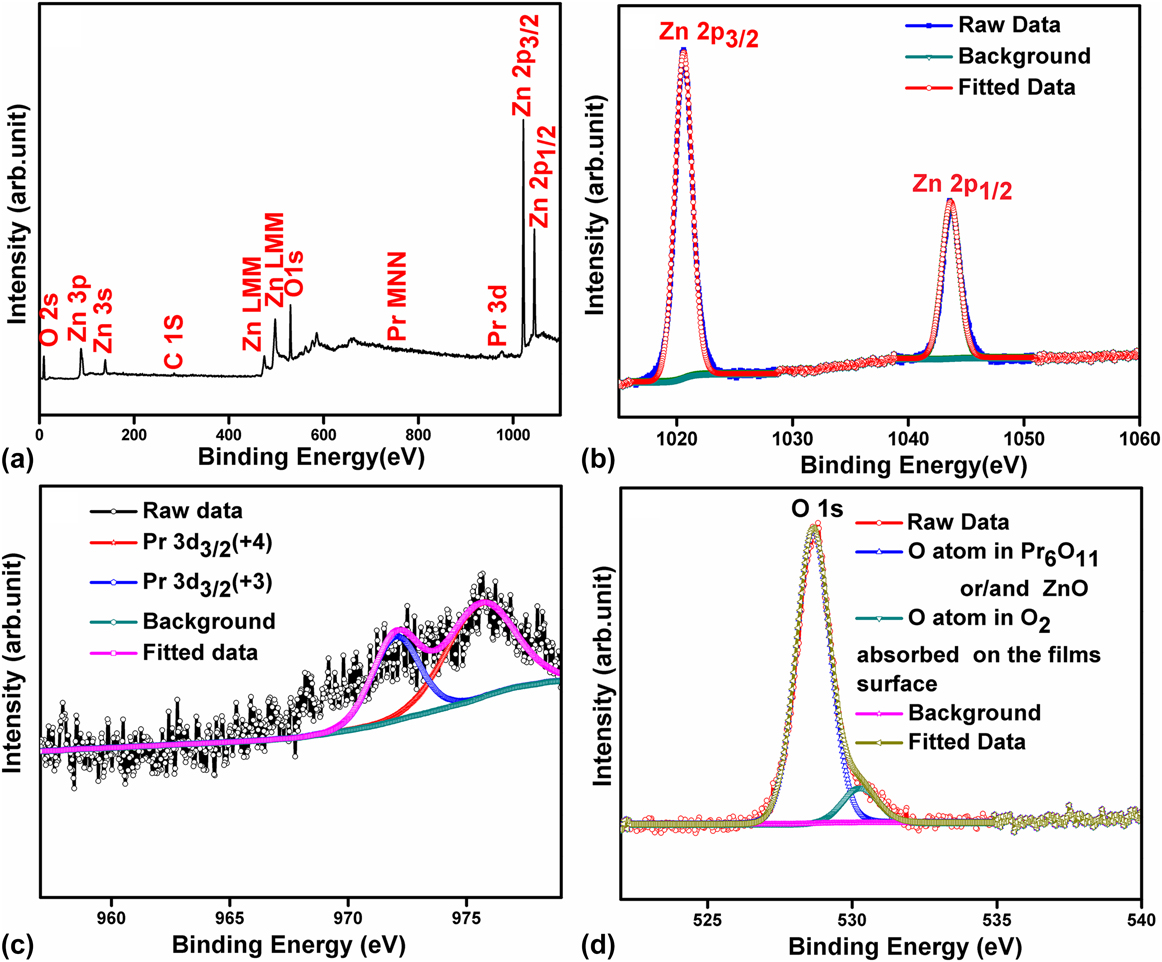
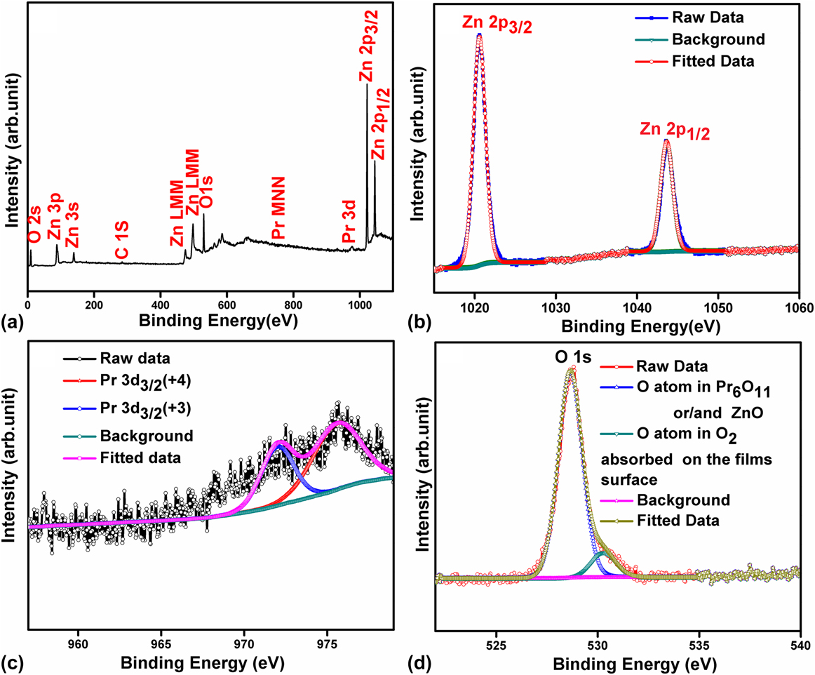
XPS spectroscopy technique is widely accepted for surface characterization and ensuring chemical composition or impurity. However, XPS only provides information about the elements in the top layer of the material, below 10 nm in the samples surface. XPS analysis indicated Zn 2p, Pr 3d, and O 1s peaks in ZnO:Pr thin films as shown in Fig. 2 and labeled as Zn, Pr, and O. Figures 2(b)–2(d) show the spectra of Zn (2p), Pr (3d), and O (1s). The full spectrum as shown in Fig. 2(a) indicates that Pr is a composite with zinc oxide films. The energy scale is calibrated using C 1s peak as the reference signal of the carbon contamination (BE = 284 eV). As shown in Fig. 2(b), two peaks of Zn 2p are detected. The peak located at 1020.6 and 1043.57 eV can be attributed to the binding energy of Zn–O bond associated with Zn 2p 3/2, and Zn 2p 1/2, respectively. These peaks are referred as the regular lattice of Zn in ZnO.Reference Armelao, Bottaro, Pascolini, Sessolo, Tondello, Bettinelli and Speghini52 The spin orbit splitting energy between two lines is 22.97 eV, lying in the nearby range of the standard reference value of ZnO.Reference Wang, Tan, Chen, Yuan, Hu, Yuan and Xiang53 The ‘O’ deconvoluted first peak has a binding energy of 528.6 eV, which can be attributed to the oxygen atoms in ZnO or Pr6O11.Reference Wang, Peng, Wang, Wang and Fu18 The peak with a higher binding energy of 530.3 eV indicates the traces of loosely bound oxygen such as adsorbed O2 on the surface ZnO:Pr.Reference Basu, Kumar, Nandy, Satpati, Saini, Kanjilal and Som54 The asymmetric Pr 3d 3/2 narrow spectrum can be deconvoluted into two peaks. The strong peak located at 975.8 eV corresponds to the Pr4+ oxidation state, while the weak peak at 972.04 eV can be assigned to the Pr3+ oxidation state.Reference Wang, Peng, Wang, Wang and Fu18 Pr3+ and Pr4+ can coexist in the Pr6O11 crystal structure; however, the difference of spin orbit splitting of energy could lead to Pr ions also incorporated into ZnO lattice.
XPS spectra of ZnO:Pr thin films. (a) Full survey, (b) Zn (2p) spectra, (c) Pr (3d) spectra, and (d) O (1s) spectra.
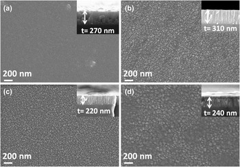
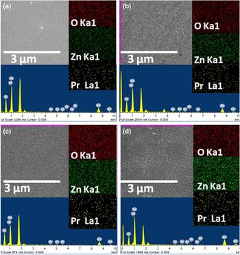
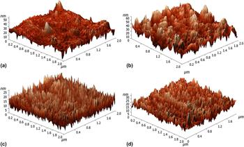
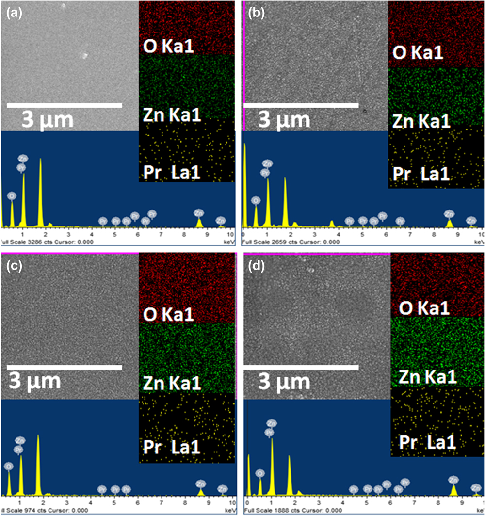
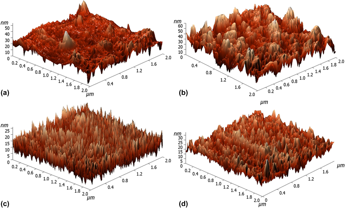
Thickness of ZnO:Pr thin films at different deposition pressures, measured by cross sectional FESEM analysis of films is shown in the inset of Fig. 3. ZnO:Pr thin films uniformly spread throughout the substrate, composed of small elongated grains and films are densely packed faceted kind of grain boundaries as can be seen in Fig. 3. However, the difference in thickness on glass and quartz substrates on similar synthesis conditions was due to different sticking coefficients and also different substrate densities of its constituents, affecting overall quality of growth, nucleation sites, defects, and surface diffusivity.Reference Phillips55,Reference Banerjee, Ghosh, Chattopadhyay, Minoura, Sarkar, Akiba, Kamiya and Endo56 However, the film morphology has shown granular shapes with clear boundaries except for Fig. 3(a). The morphology of sputter deposited ZnO:Pr films vary with sputtering deposition pressure and underlying substrate in terms of grain growth as well as the shape of grains. Large grain size is observed due to the fact that the kinetic energy is changed at high sputtering pressure and deposition rate could lead to more agglomeration of particles. The coarsening of grains and intergrain connections are more significant in Fig. 3(d). The composition of films was measured by EDS. EDS mapping along with EDS spectra is shown to ensure film purity and distribution of elements throughout the scanning area (Fig. 4). EDS mapping shows a uniform distribution of elements Pr, Zn, and O in the scanned area of films. The at.% of Pr, Zn, and O of ZnO films is given in Table I and thin films are found to be oxygen-rich. The SEM and XRD results of thin films are in accordance with each other and found to be crystalline and columnar growth at high sputtering pressure. The root mean square roughness of the ZnO:Pr thin films was measured by atomic force microscopy operated in the semicontact mode of region 2 × 2 µm as shown in Fig. 5. The distributions of grains are distinct, elongated particles and length of grains increased at 10 mtorr on the glass substrate and fused quartz substrate. The grains are elongated and thicker in size at 10 mtorr sputtering deposition pressure and showed higher RMS roughness as can be seen from Table II. The same kind of observation is established by FESEM micrographs where grain size increases at 10 mtorr sputtering depositions. Sputtering deposition conditions strongly influence in terms of kinetic energy of ad-atoms and the deposition rate, showing higher roughness of films at high sputtering pressure.
FESEM images of ZnO:Pr thin films deposited at (a) 5 mtorr @ glass substrate, (b) 10 mtorr @ glass substrate, (c) 5 mtorr @ fused-quartz substrate, and (d) 10 mtorr @ fused-quartz substrate.

EDS Mapping of ZnO:Pr thin films deposited at (a) 5 mtorr @ glass substrate, (b) 10 mtorr @ glass substrate, (c) 5 mtorr @ fused-quartz substrate, and (d) 10 mtorr @ fused-quartz substrate.
AFM images of ZnO:Pr thin films deposited at (a) 5 mtorr @ glass substrate, (b) 10 mtorr @ glass substrate, (c) 5 mtorr @ fused-quartz substrate, and (d) 10 mtorr @ fused-quartz substrate.
Mechanical properties and roughness of ZnO:Pr thin films.

C. Nanomechanical and scratch crack propagation resistance of ZnO:Pr thin films
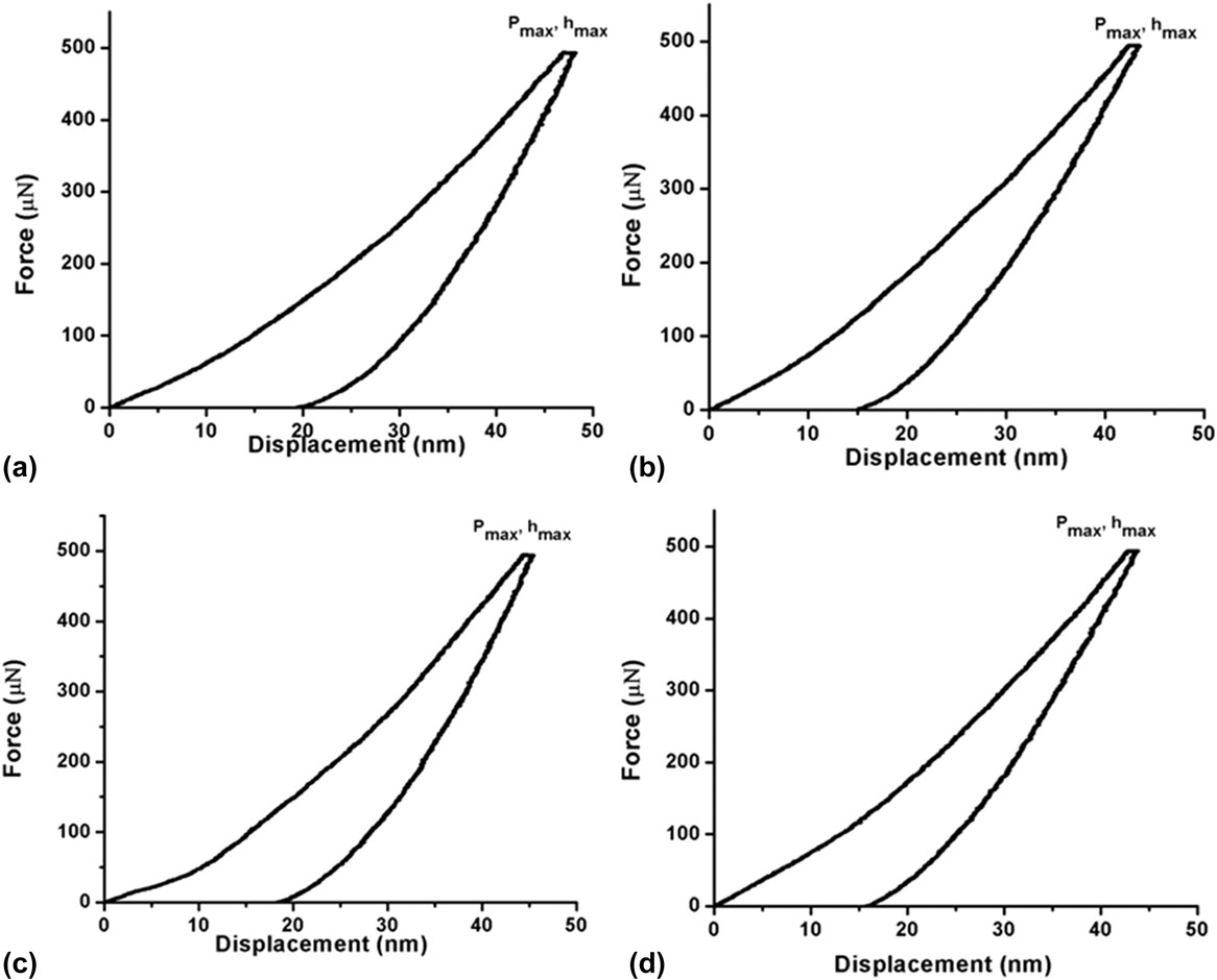
ZnO thin films show variations in mechanical properties depending upon the size scale as well as crystalline growth and orientations of films.Reference Sung, Huang and Chen57 Defect free ZnO thin films usually follow higher hardness than bulk depending upon the microstructure.Reference Bhardwaj, Chowdhury and Jayaganthan5,Reference Sung, Huang and Chen57–Reference Navamathavan, Kim, Hwang, Park, Hahn, Lee and Kim59 In addition, the ionic and covalent bonding in the lattice affects the mechanical properties as well as failure in the films is altered by introducing a foreign element/impurity in the lattice, which leads to the formation of a new defect state.Reference Kucheyev, Bradby, Williams, Jagadish and Swain25 The Pr ion introduced in the ZnO lattice could result in similar change and influence its mechanical properties. The experimental observation during loading–displacement–unloading segments of ZnO:Pr thin films at different deposition pressures are shown in Fig. 6. Indenter loading is increased from 0 to 500 µN and it penetrates in the material surface up to penetration depth depending upon elastic–plastic nature of materials. The penetration depth of the indenter should not exceed in the sample beyond ≤t/10 (t is the film thickness) to avoid substrate influence. However, it is valid to the samples where thickness of the coatings is ≥1 µm.Reference Lin, Jeong, Kim and Myoung60 Also, the coating and substrate is a composite system and the substrate has a huge effect on the film mechanical properties; however, with the increase of penetration depth, the substrate effect becomes more pronounced due to its closer proximity with the indenter.Reference Kataria, Goyal, Dash, Sandhya, Mathew and Tyagi61 It is observed that hard film on the soft substrate is more prone to be affected by the substrate at lower penetration depth.Reference Kataria, Goyal, Dash and Tyagi62 However, mechanical properties of zinc oxide thin films deposited on glass substrates were least affected when penetration depth less than 20% of thickness and inhomogeneous flow or serration, pop-ins during loading–displacement observed indicating plastic deformation.Reference Zhao, Zhou, Liu, Zhao, Wang, Xiang, Liu, Han, Zhang and Chen33,Reference Huang and Chang36 The thicknesses of the films were 220, 240, 270, and 310 nm given in Fig. 3. The indentation displacement is kept less than 20% (t/5) to total thickness ‘t’ to minimize the substrate effect and avoid shallow indentation and indentation size effect, which is more pronounced at shallow indentation depths.Reference Roy63 Uncoated substrates were probed and their mechanical properties provided in the Supplementary Material, Fig. S1.
Loading–unloading curves of ZnO:Pr thin films deposited at (a) 5 mtorr @ glass substrate, (b) 10 mtorr @ glass substrate, (c) 5 mtorr @ fused-quartz substrate, and (d) 10 mtorr @ fused-quartz substrate.

The indentation was performed on thin films at several locations with same load and loading rate. It is clear from Fig. 6 that ZnO:Pr thin films having a loading/unloading curve without discontinuities/pop-in (≥2 nm) during the penetration of the indenter indicate better adherence to the substrate and rules out fracturing or delamination during indentation.Reference Bull22,Reference Patriarche, Glas, Le Roux, Largeau, Mereuta, Ougazzaden and Benchimol64 Major discontinuities or sudden jump during penetration of the indenter could arise due to incorporated defect sites but minor discontinuity as collective event of slip and propagation can be inhibited by grain boundaries or at the substrate.Reference Navamathavan, Kim, Hwang, Park, Hahn, Lee and Kim59,Reference Li, Van Vliet, Zhu, Yip and Suresh65 The plastic deformation and fracture events are influenced by the dislocation dynamics through active slip system depending upon the stored energy and localized stress induced by the indenter tip in the material.Reference Li, Van Vliet, Zhu, Yip and Suresh65 Multiple events of pop-in were reported in ZnO as a consequence of initiation of slip and dislocation burstReference Kucheyev, Bradby, Williams, Jagadish and Swain25 depending upon the loading rate.Reference Fang, Chang and Lin31 Average mechanical properties of ZnO:Pr films are given in Table II after multicurve analysis. There is a slight variation in the hardness, but enhanced hardness at 10 mtorr sputtering deposition pressure is due to better crystallinity and grain size of thin films.Reference Musil66 Also, the hardness of the ZnO thin films is slightly higher at 10 mtorr sputtering deposition pressure (9.89 ± 0.14 GPa) on the glass substrate. The highest crystallinity in the polar plane accounts for higher hardness observed in ZnO as compared to a-plane or m-plane depending upon the ease of slip events.Reference Juday, Silva, Huang, Caldas, Prioli and Ponce28 ZnO:Pr thin films have shown high Young’s modulus (112.12 ± 3.45) GPa deposited at 5 mtorr deposition pressure due to the presence of a-plane and m-plane crystalline orientations.
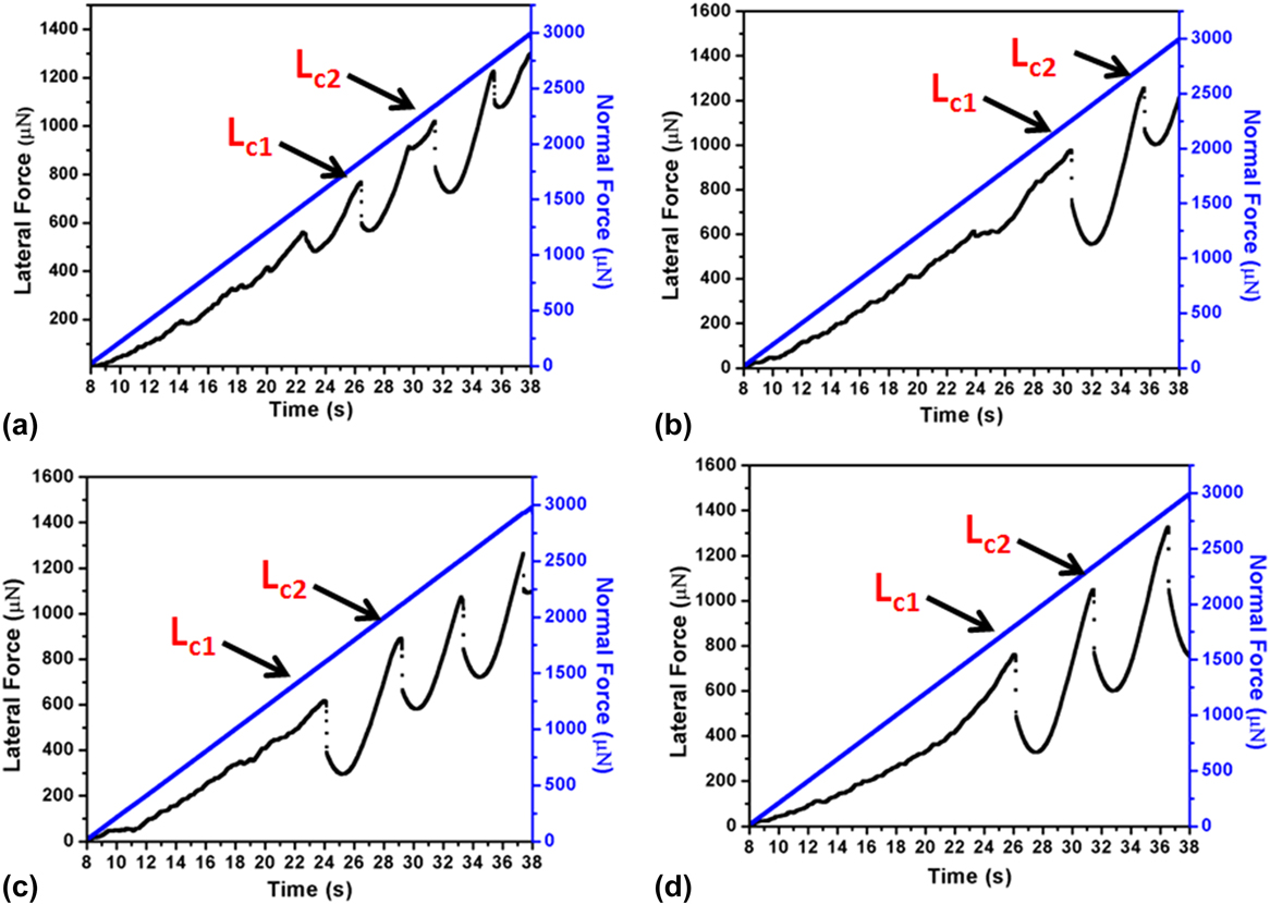
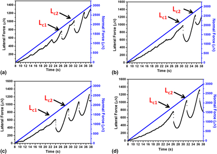
Scratch scan is recorded as frictional forces indicating elastic–plastic interaction of the loading and sliding indenter as well as the event of failure. The elastic interaction is observed in the beginning of the scratch test at lower normal load; however, the increased applied forces deform materials plastically. The failure events are correlated with adhesive/cohesive interaction which primarily depends on the shear force per unit area and interfacial shear stress between the film and substrate.Reference Benjamin and Weaver67 However, scratch behavior has changed as a consequence of incorporation of Pr ions on Zn lattice sites as compared to pure ZnO.Reference Bhardwaj, Chowdhury and Jayaganthan5,Reference Bhardwaj, Chowdhury and Jayaganthan68 Progressively increasing normal force applied from 0 to 3000 µN load exhibiting failure event is responsible for sudden discontinuity in the lateral force curve at lower L c1 and upper critical force at L c2 as given in Table II and Fig. 7. The Pr-doped ZnO thin films has fractured after bearing significant plastic deformation and the scratch curve is smooth before discontinuity occurred as shown in Fig. 7. The smooth and oscillation-free curves observed in lateral force indicate good scratch resistance before fracture and failure. The initial or lower critical load is a complex phenomenon, which is not considered as complete failure of films as it depends on the upper critical load. Difference in upper and lower critical load significantly affects the fracture toughness of the films.Reference Zhang, Sun, Fu and Du69 Lower cohesive strength of films causes lower scratch resistance and therefore deteriorates overall strength of thin films. The scratch crack propagation resistance indicates durability and toughness of ZnO:Pr films. The initial critical load L c1 is believed to be initiation for the crack event and propagation and upper critical load L c2 as complete failure. The parameter as (L c2–L c1) represents the scratch toughness of the ZnO:Pr thin films. The scratch crack propagation resistance parameter (CPRS) in Eq. (3) represents resistance to crack initiation and propagation and qualitative response of coatingsReference Kabir, Munroe, Zhou and Xie70 is expressed as
 $${\rm{CPRs}} = {L_{{\rm{c}}1}}\left( {{L_{{\rm{c}}2}} - {L_{{\rm{c}}1}}} \right)\quad .$$
Frictional forces of ZnO:Pr thin films deposited at (a) 5 mtorr @ glass substrate, (b) 10 mtorr @ glass substrate, (c) 5 mtorr @ fused-quartz substrate, and (d) 10 mtorr @ fused-quartz substrate.
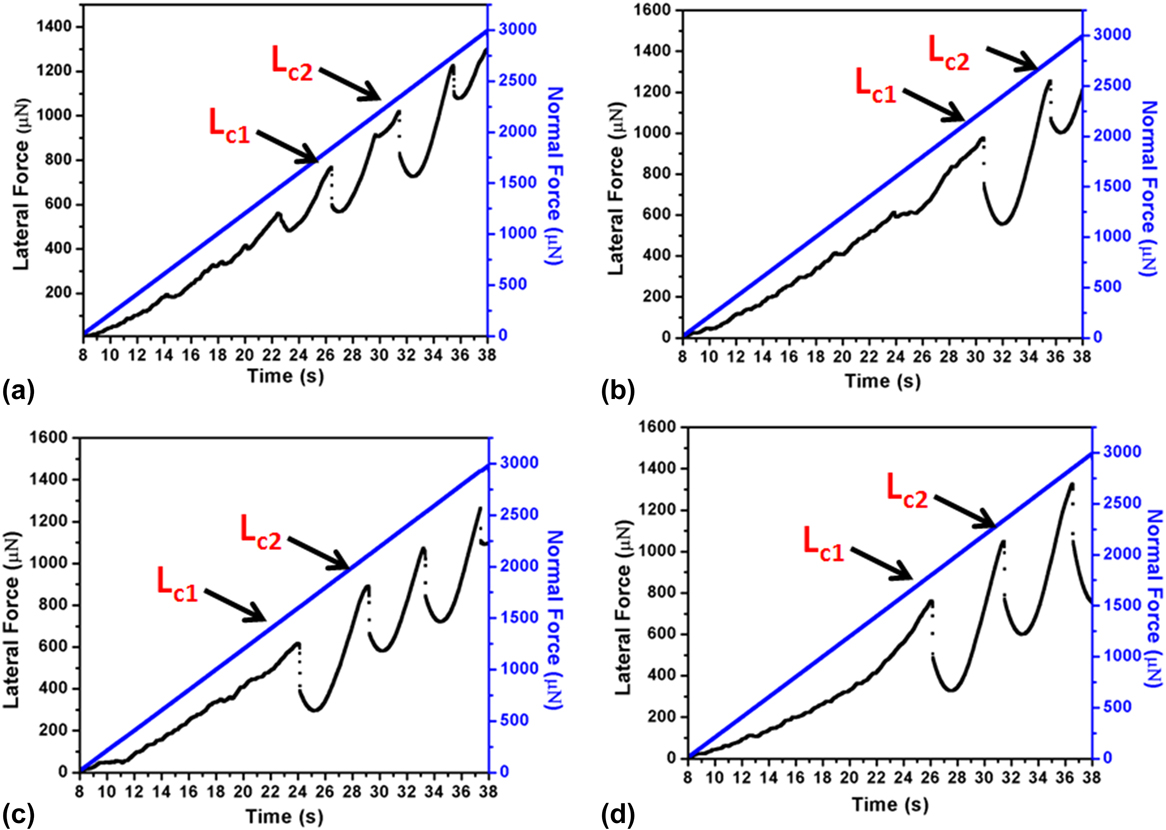
The CPRs ratio of ZnO:Pr films are given in Table II and observed higher CPRs for the films with higher crystallinity at 10 mtorr pressure. The films’ strength can be predicted by using H/E ratio (hardness/Young’s modulus) termed as plasticity index given in Table II.Reference Benjamin and Weaver67 Higher H/E materials are expected to have better wear resistant properties due to small accumulated strain energy.Reference Ni, Cheng, Lukitsch, Weiner, Lev and Grummon71 The higher H/E ratio observed in the present work indicates better wear resistance properties at 10 mtorr pressure depositions in accordance with CPRs.
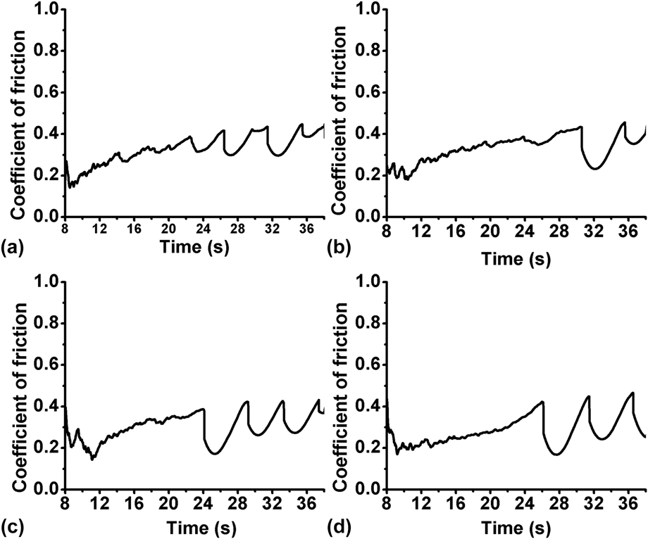
The ratio of lateral forces to normal forces gives friction coefficient during scratch which provides insight into performance of coatings in tribological applications.Reference Sung, Huang and Chen57 It can be observed from Fig. 8 that the friction coefficient has varied from 0.2 to 0.4 and as the friction coefficient increased beyond 0.4, a sudden fall or breakdown is observed. The friction curve provides nature of contact between sliding indenter on thin films and stress distribution. Initially, the scratch section experiences lower contribution of plowing force and more elastic interaction will occur but as the normal load increases, grain boundary resistance to scratch, roughness, and several other factors come into play before fracturing the films. Minor discontinuities or oscillations initially were considered as the effect of different scratch resistances at grain boundaries which is correlated with different crystalline orientations to grain growth.Reference Bhushan and Li72 The coefficient of friction lies between 0.2 and 0.4, in accordance with the reported values in the literature.Reference Jian, Teng, Yang, Lai, Lu, Chang and Ju73
Coefficient of friction of ZnO:Pr thin films deposited at (a) 5 mtorr @ glass substrate, (b) 10 mtorr @ glass substrate, (c) 5 mtorr @ fused-quartz substrate, and (d) 10 mtorr @ fused-quartz substrate.

IV. CONCLUSION
Highly crystalline Pr-doped ZnO thin films were successfully deposited using DC sputtering in the present work. The mechanical properties and tribological behavior of films were investigated and the following conclusions are drawn.
(1) There is no evidence of XRD peaks related to Pr or Pr6O11 in thin films and therefore, it is expected that Pr acquires substitutional positions in the ZnO lattice.
(2) The FESEM and AFM confirm the formation of the nanostructured morphology of grains in ZnO:Pr films, which depend on synthesis condition as well as the substrate material. The RMS roughness and intergrain connections are more pronounced for the films deposited at 10 mtorr sputtering pressure.
(3) The nanoindentation study of ZnO:Pr films has shown the high hardness (9.89 ± 0.14) GPa, Young’s modulus (112.12 ± 3.45) GPa, highest initial critical load 2250.5 µN, and CPRs ratio 11.34 × 10⁵, for the films deposited, indicating good adherence of films. However, there is a slight difference between hardness and Young’s modulus of the films on both the substrates but the critical load for coating fracture suggested a good scratch resistance on the glass substrate attributed to better crystallinity.
(4) The XPS result provided the surface analysis and confirms the presence of Pr ions and it is in accordance with EDS mapping with uniform presence of Pr ions throughout the scanning area. Also, Pr 3d in thin films with the XPS peak were deconvoluted, located at 975.8 eV corresponding to the Pr4+ oxidation state, while the weak peak at 972.04 eV can be assigned to the Pr3+ oxidation state, which is also relevant to Pr ions being composite with the zinc oxide films.
Supplementary Material
To view supplementary material for this article, please visit https://doi.org/10.1557/jmr.2018.154.
ACKNOWLEDGMENT
The authors would like to thank Prof. Ramesh Chandra for providing sputtering facility at Institute Instrumentation center, IIT Roorkee, India, and Material Research Center, MNIT Jaipur, India, for XPS analysis.