Introduction
The rapid evolution of future wireless networks necessitates higher available bandwidth and data rates to enable applications and large-scale data transmission. A 3 GHz licensed spectrum is expected to be allocated to the 40 GHz band, as reported by recent projections from the Federal Communications Commission to support data rates exceeding 1 GS/s. This trend has driven intensive research on millimeter-wave (mm-wave) integrated devices and circuits featured by wide bandwidth, low phase noise, and minimal spurious tones. The source generator, which is typically a phase-locked loop (PLL), is one of the most essential components in recent development of mm-wave transceivers, as it is responsible for generating high-frequency stable and tunable carriers required for wireless connectivity. However, the performance of mm-wave PLLs is fundamentally constrained by their phase noise and spurious emissions, which directly limit the attainable data rates [Reference Ek, Påhlsson, Elgaard, Carlsson, Axholt, Stenman, Sundström and Sjöland1]. To encourage higher order modulation schemes such as 512/1024-QAM in six-generation (6G) networks, mm-wave PLLs must achieve excellent jitter characteristics, strong suppression of spurious tones, and minimized adjacent- and self-channel interference to suppress out-of-band emission and aliased energy [Reference Yang, Chen, Yang, Mak and Martins2–Reference Shahramian, Hart, Tomkins, AC, Garcia, Chevalier and Voinigescu8].
In integrated mm-wave PLLs, the existing low-quality-factor passive components results in considerable degradation of jitter performance due to the high phase noise of the voltage-controlled oscillator (VCO). Considering the fact that the phase noise of the VCO is high-pass filtered by the loop, the resulting root-mean-square (RMS) phase error can be expressed as a function of the single-sideband phase noise, the frequency offset ∆f, and the PLL loop bandwidth fBW [Reference Shahramian, Hart, Tomkins, AC, Garcia, Chevalier and Voinigescu8]:
 \begin{equation}\sigma _\phi ^{{\text{PLL}}} = \Delta f\sqrt {\frac{{\pi \cdot S_{{{SSB}}}^{{{VCO}}}}}{{{f_{{{BW}}}}}}} .\end{equation}
This relationship highlights the need for a sufficiently wide loop bandwidth to effectively suppress VCO noise. While increasing the loop bandwidth mitigates more of the VCO phase noise, it simultaneously extends the PLL roll-off frequency, which diminishes the rejection of reference spurs. Consequently, a fundamental trade-off arises between achieving low VCO-induced jitter and maintaining adequate spurious suppression.
To address the above challenges, this paper introduces a phase detector (PD), referred to quadrature-phase spurious-tone-canceling PD (QSC-PD). The introduced QSC-PD provides an extra design degree of freedom particularly for type-I PLLs, relaxing the aforementioned trade-off. The key idea is to employ a complementary current-reuse phase detection path, where the spurious component introduced by the auxiliary path cancels that of the primary path without reducing fBW. Any residual mismatch between the two paths results in a disturbance current at four times of the reference frequency (i.e., 4f REF), which is further attenuated by the PLL low-pass filter (LPF). Consequently, both wide fBW and low spurious levels can be attained simultaneously. Additionally, the QSC-PD architecture inherently supports fast VCO lock acquisition.
PDS with spurious attenuation techniques
A conventional type-I single-loop PLL exhibits unconditional stability and is regarded as a strong candidate for realizing the wide loop bandwidth (fBW) necessary in high-frequency mm-wave applications [Reference Sharkia, Mirabbasi and Shekhar9]. One common method for suppressing reference spurs is to suppress the large output voltage disturbance appeared at the XOR-gate PD by narrowing fBW. However, this approach reduces the capture range, potentially preventing the PLL from achieving phase-lock. Conversely, when a wide loop bandwidth exceeding 10 MHz is applied – allowing broader capture capability and stronger suppression of VCO noise – the spurious level may become comparable to the VCO output power itself [Reference Kong and Razavi10].
Recent PDs
Classic type-I PLLs that rely on XOR-gate PDs generally suffer from high spurious tone levels even when operating with multi-gigahertz reference frequencies (f REF). For example, in paper [Reference Liu, Trasser and Schumacher11], despite using a f REF/fBW ratio greater than 30, the reference spur was only reduced to −33 dBc. To mitigate this, a continuous-time twin-T RC filter with notch response has been employed after the XOR-gate output [Reference Lin, Hu and Gupta12]. The twin-T topology merges a high-pass filter and LPF, creating a notch at the reference frequency. While this approach reduces the spurious level at f REF without greatly incurring noise to the loop, it degrades the loop stability and requires a longer settling times. In fact, spur suppression beyond 7 dB compromises the phase margin. With this technique, a spurious tone level of −62 dBc was achieved, but only with a narrow loop bandwidth of less than 100 kHz.
A filter can be designed to isolate the VCO tank from the PD-induced transitions. One example is the master-slave sampling filter (MSSF) [Reference Kong and Razavi10]. It generates notches at f REF and its harmonics, attenuating the reference spurious level without greatly reducing the loop bandwidth. Nevertheless, the second sampling switch has to carry large transient currents, which can induce considerable flicker noise. To counteract this, the device must be oversized, though this increases charge injection, clock feedthrough, and leakage, resulting in substantial ripple. Additionally, the loop bandwidth depends on the capacitor ratio C 2/C 1. Even with large capacitors, spurious levels remain at −46 dBc. A subsequent harmonic trap circuit using LC equivalences can further reduce spurs to −65 dBc, but this also raises phase noise peaking by 1 dB and requires off-chip calibration.
Another approach eliminates the need for a reference buffer has been reported in paper [Reference Yang, Chen, Mak and Martins13]. The sampling PD directly samples the external reference clock. In the PD, devices arranged in a complementary manner can mutually cancel charge injection and clock feedthrough, thereby suppressing the voltage disturbance. Such a design achieved a spurious tone of −63.9 dBc with a wide loop bandwidth of ∼20 MHz. However, the PD gain depends on the sinusoidal reference amplitude, and additional first-order RC filters are required in both sampling paths to suppress ripple and linearize K PD, which narrows the capture range. Furthermore, effective cancellation of charge injection and feedthrough depends on precise device matching, making the design sensitive to process variation and temperature shifts. Meanwhile, phase noise peaking near the loop bandwidth also degrades the overall integrated jitter.
Spur reduction techniques have also been applied to type-II PLLs. For instance, a charge-pump PLL (CP-PLL) was proposed with feedback in the CP to mitigate current mismatches between NMOS pull-down and PMOS pull-up devices, attaining a −61 dBc spurious level but only with a very narrow loop bandwidth of ∼500 kHz [Reference Abdulaziz, Forsberg, Tormanen and Sjoland14]. Another work [Reference Elsayed, Abdul-Latif and Sanchez-Sinencio15] introduced a block capable of spur-frequency boosting between the PFD and CP, shifting the disturbance rate to a higher frequency where loop gain is weaker, thereby improving spur suppression. However, this block consumes significant power at high reference frequencies, which are often used for attenuating in-band noise amplification of a PLL [Reference Liu, Trasser and Schumacher11, Reference Ikeda, Ito, Kasamatsu, Ishikawa and Obara16, Reference Kang, Chien and Niknejad17]. The resulting loop bandwidth in paper [Reference Elsayed, Abdul-Latif and Sanchez-Sinencio15] was limited to ∼335 kHz for spur suppression below −60 dBc, which is not sufficiently wide to attenuate the VCO phase noise.
In paper [Reference Wu, Yao, Godbole, Ni, Chiang, Han, Zuo, Verma, Lu, Son and Cho18], a sampling PLL employing an SPD was proposed as an alternative to designs relying on high-resolution multi-bit time-to-digital converters (TDCs). While this avoids TDC-induced quantization errors, the limited linear range of the SPD still demands an RC filter to suppress spurs. As a result, a frequency-tracking loop (FTL) is needed to accelerate the frequency acquisition. Furthermore, thick-oxide transistors are used in the sample-and-hold switches to stabilize ON-resistance, requiring non-overlap pulse generators level-shifted to a higher supply voltage, which increases reference path power consumption. Sub-sampling PLLs [Reference Kim, Yoon, Lim, Lee, Cho, Seong and Choi19, Reference Kar, Mohapatra, Hoque and Heo20] and injection-locked PLLs [Reference Tsai, Sheen, Hsu, Chang and Staszewski21, Reference Zhang, Narayanan, Herdian, Liu, Wang, Shirane and Okada22] have demonstrated low-jitter (e.g., σ rms < 100 fs) performance yet typically exhibit poor spur performance, around −50 dBc.
In summary, existing PD architectures can suppress spurious tones while maintaining favorable jitter performance, but they inevitably introduce drawbacks: (1) extra poles in the loop that reduce phase margin, (2) increased phase noise peaking, or (3) restricted acquisition ranges that necessitate auxiliary FTLs for locking.
PD with spurious tone canceling
The MSSF and the CRS-PD simultaneously provide wide fBW and spurious suppression. However, both primarily depend on filtering mechanisms to mitigate spurious tones. As the sampling switches inherently generate spurs at f REF and its harmonics, it is beneficial to analyze switch output component including the polarity and amplitude of each harmonic term. When two periodic square waves with frequencies f 1 and f 2 are applied to a switch, the resulting output voltage contains the following harmonics:
 \begin{equation}{V_1}(t) = A\left[ {\frac{1}{2}\sin \left( {2\pi \left( {{f_1} - {f_2}} \right)t} \right) + \frac{1}{2}\sin \left( {2\pi \left( {{f_1} + {f_2}} \right)t} \right){\text{ + }} \bullet \bullet } \right]{\text{ }}\end{equation}
where A is a constant proportional to the square of the input signal swing. If the design objective is to cancel harmonics of the reference frequency while preserving the first term, which is also a near-DC term, a straightforward solution is to subtract the quadrature version of (2) like the image injection in a harmonic rejection mixer [Reference Razavi23], yielding
 \begin{equation}\begin{array}{*{20}{l}}
{{y_2}(t) = A[\sin \left( {2\pi \left( {{f_1} - {f_2}} \right)t} \right) + \frac{1}{3}\sin \left( {2\pi \left( {{f_1} + 3{f_2}} \right)t} \right)} \\
{ - \frac{1}{3}\sin \left( {2\pi \left( {{f_2} + 3{f_1}} \right)t} \right) + \bullet \bullet ]}
\end{array}.\end{equation}
In this way, the second harmonic is canceled perfectly, and the remaining higher order terms (e.g., the fourth harmonic) are either neutralized by the same way or substantially attenuated by the PLL LPF. Importantly, introducing the quadrature phase does not hinder the settling of the PLL, as the term sin [2π(f 1 − f 2)t] continues to drive the feedback loop, correcting the frequency error Δf = |f 1 − f 2|.
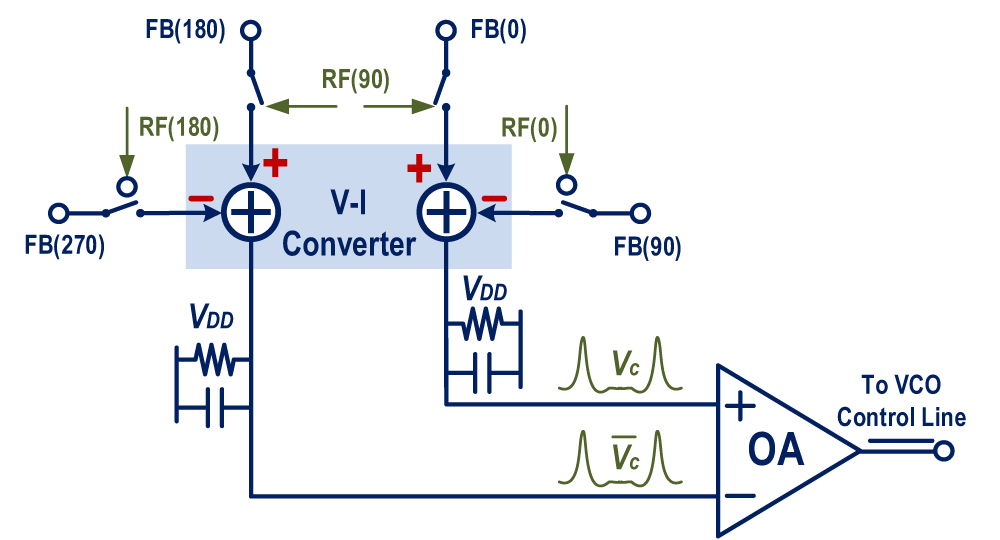
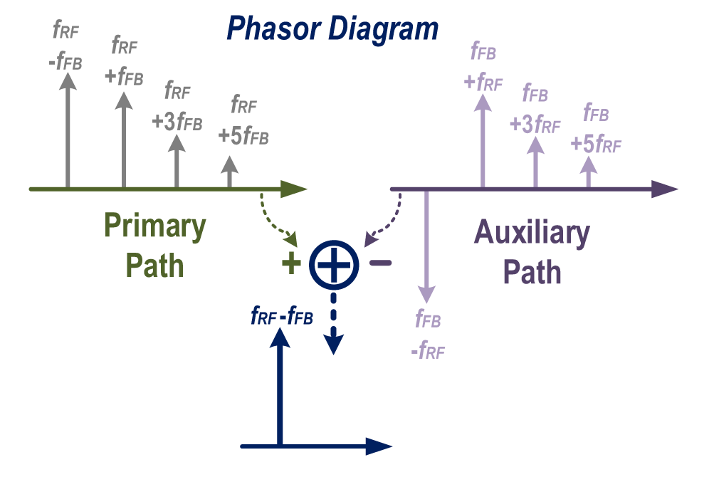
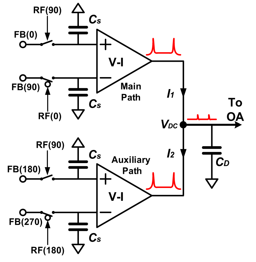
The above observation motivates the design of a spurious-tone-canceling PD, illustrated in Fig. 1. The detector comprises two pairs of switches: the quadrature reference signals are denoted as RF(0), RF(90), etc., while FB(0), FB(90), etc., represent the quadrature feedback outputs from the frequency divider. A narrowband (bandwidth ≈10 kHz) yet high gain (39–48 dB, tunable) operational amplifier (OA) senses the PD near-DC output voltage and converts it to current to drive the VCO. The spurious-tone-canceling PD functions such that spurs generated by one switch pair are neutralized by those from the other pair at the OA input. For instance, when RF(0) and FB(180) are in phase, their in-phase spurs cancel, resulting in an OA output current free of ripple, assuming full circuit symmetry. Figure 2 shows the phasor diagram illustrating the spurious tone canceling, where only the near-DC component is preserved. In the case of f REF = f DIV, all spurious tones can be effectively suppressed due to mutual canceling.
Concept of dual-path spurious tone canceling.

Phasor diagram of Figure 1.

From another perspective, the quadrature replica introduces glitches at 90° relative phase to the main path, causing the OA to generate four evenly spaced glitches to the VCO control voltage per reference cycle. Thus, the spurious frequency is effectively boosted from 2f REF (differential operation) to 4f REF (quadrature operation), where it experiences stronger LPF attenuation, similar to the frequency-boosting method described in paper [Reference Elsayed, Abdul-Latif and Sanchez-Sinencio15]. Compared with that technique, however, this approach is simpler and more power-efficient. Notably, the auxiliary spurious-tone-canceling path does not introduce additional poles, thereby preserving loop stability.
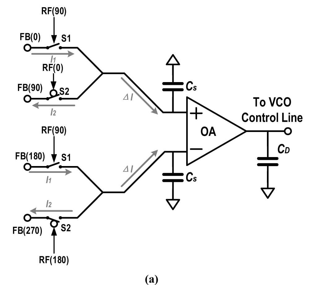
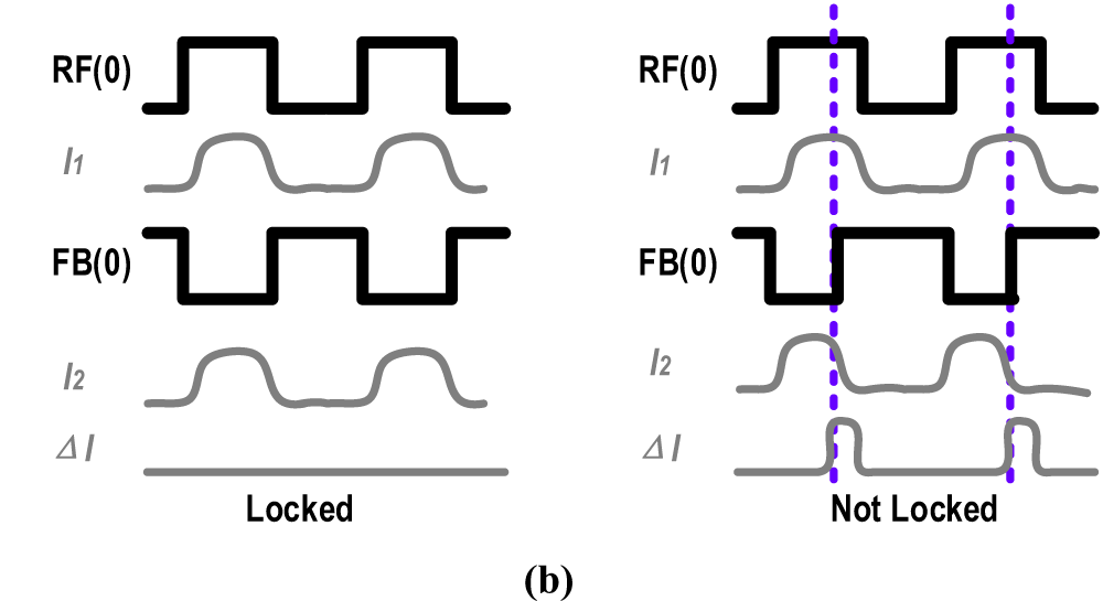
Nonetheless, implementing the above spurious-tone-canceling PD requires two parallel switch pairs, which doubles the PD static current, and the loading resistor introduces additional noise to the PD output. To overcome these limitations, the architecture is refined into the topology shown in Fig. 3. In this design, the auxiliary phase-detection path bypasses the ripple current introduced by the primary path when I 1 = I 2. During phase alignment, I 1 ≠ I 2, so the capacitor Cs is charged by the net current ΔI = |I 1 − I 2|, enabling the OA to deliver a proportional current into the PLL LPF. Figure 4 illustrates the spurious-tone-canceling process. Here, the spurious current from switch S2 neutralizes that of the switch S1, thereby canceling the spurious tone. When circuit mismatch occurs (i.e., Fig. 4), where I 1 ≠ I 2 at lock, the PD produces a phase offset between the divider feedback and reference clock, but still neutralizing the capacitor charge at most extend. Unlike earlier sampling PDs [Reference Yang, Chen, Yang, Mak and Martins2, Reference Kong and Razavi10, Reference Yang, Chen, Mak and Martins13], a non-overlap generator is unnecessary, as cancellation is achieved by mutual current compensation rather than master-slave sampling.
Concept of spurious tone canceling without doubling the PD static current.

Timing diagram of spurious tone canceling of Figure 3.

In practice, spurious cancellation is conducted in the current domain. As shown in Fig. 5, differential switch S1 and S2 drives a V-to-I converter, while switch S3 and S4 drives another one. Each V–I converter transforms the sampled voltage across Cs into current. Likewise, the glitch currents from the primary path I 1 is neutralized by its counterparts I 2 from the auxiliary phase-detection path, as both introduce disturbances in phase.
Illustration of spurious-tone-canceling technique performed in complementary fashion.

The PLL spurious tone level can be quantified in terms of the disturbance on the VCO control voltage ΔV ctrl as given in paper [Reference Lin, Hu and Gupta12]:
 \begin{equation}{\text{Spu}}{{\text{r}}_{{\text{PLL}}}} = 20\log \left( {\frac{{K{}_{{\text{VCO}}}^{} \times \Delta {V_{{\text{ctrl}}}}}}{{2\pi \times {f_{{\text{REF}}}}}}} \right).\end{equation}
If current mismatches exist between the two phase-detection paths, the imbalance current ΔI exacerbates spurious suppression, as analytically evaluated from Fig. 6. Though reducing fBW naturally helps suppress mismatch-induced spurs, utilizing a bigger capacitor CD at the PD output also lowers the spurious level with minimal effect on the fBW.
Analytical spurious tone level against fBW, ΔI, and CD.

Proposed QSC-PD
PD topology
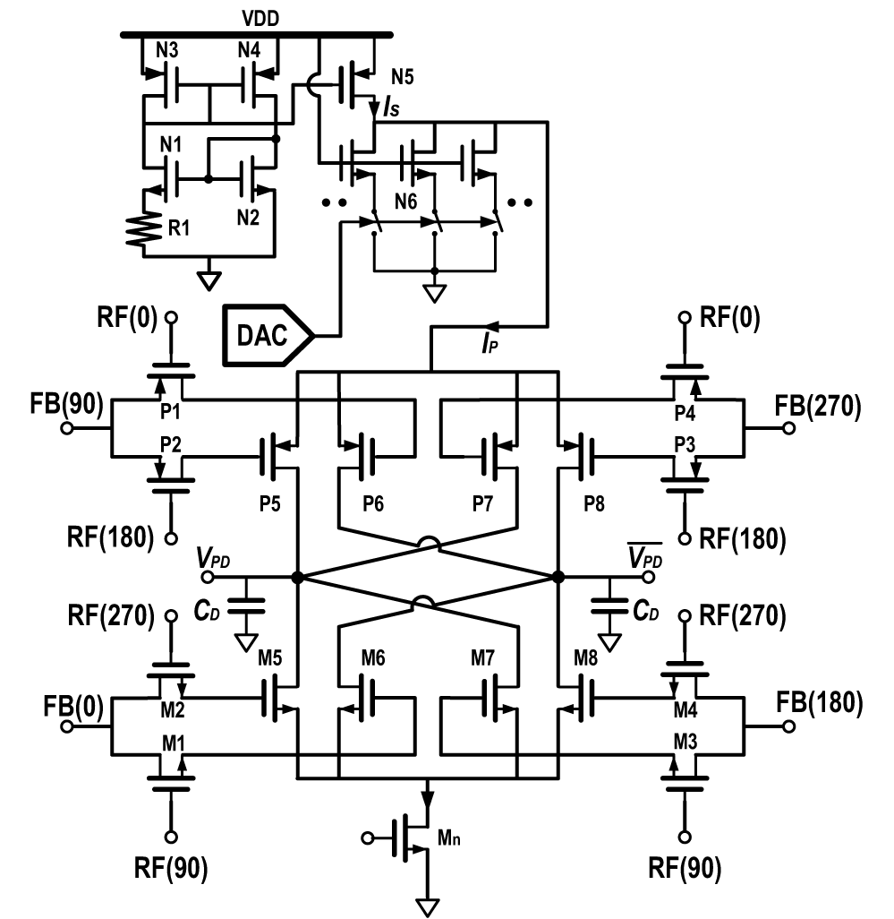
Figure 7 illustrates the QSC-PD for spurious cancellation. The detector utilizes quadrature switches (P1–P4) such that, when driven by the reference clock, the divider output voltage is sampled and directed to the V–I converter realized by P5–P8, which subsequently charges the load capacitor CD. Once the switch is deactivated, the existing divider output voltage is preserved on the switch drain capacitor. To maintain the same static power, transistors M1–M4 serving as the sampling switches, as well as transistors M5–M8 performing the V–I conversion, operate in quadrature with the PMOS devices P1–P4 and P5–P8, respectively. The currents generated by both paths combine at the capacitor CD. Since complementary transistors in each pair conduct simultaneously for a quarter cycle, the spurious contributions are mutually canceled while preventing short-circuit paths. This current-reuse strategy allows the NMOS branch to share power with the PMOS branch, thereby burning only half the power of dual-path sampling PDs (e.g., Fig. 1).
Circuit implementation of the QSC-PD.

Transistor N1–N5 establishes a supply-insensitive circuit, providing stable current to the PD in the presence of supply perturbation. The current digital-to-analog converter (DAC) governs the current Ip injecting into the PMOS branch, whereas the current source Mn defines the current In injecting to the NMOS branch. The balance of both paths can be ensured by configuring the current DAC digitally in this work.
Spurious tone canceling
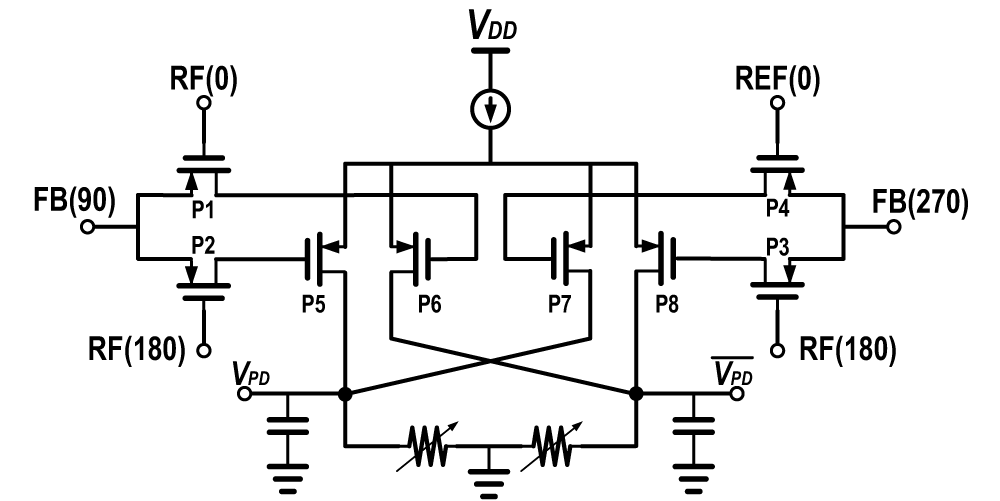
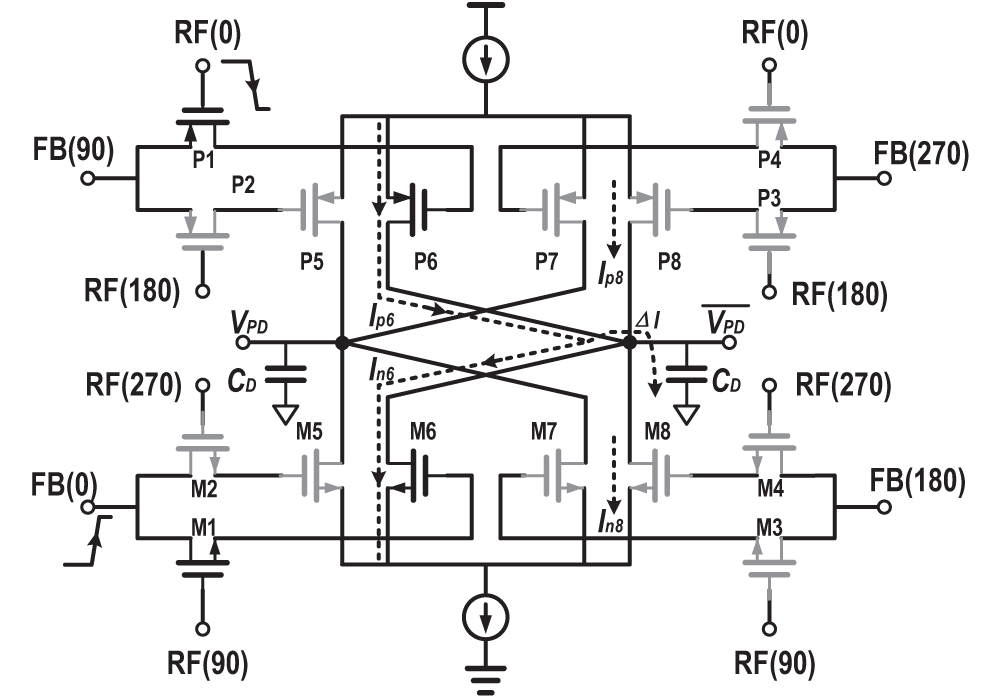
Classic PD without spurious cancelling is illustrated in Fig. 8. Here, spurious cancelling is achieved by neutralizing the charges from the PMOS and NMOS paths. As illustrated in Fig. 9, for instance, when RF(0) falls, FB(90) activates P1 and P6 to inject current I p6, which is compensated by M1 and M6 supplying current I n6. Similarly, other device pairs (e.g., P3–M8, P7–M5) cancel spurious charges across cycles. Consequently, the PD ultimately generates a near-DC voltage at the output.
Half-circuit of the QSC-PD for comparison.

Current-reuse and spurious tone canceling by the QSC-PD.

If the PLL is unlocked, RF(0) and FB(180) exhibit a phase offset, producing a net current (i.e., ΔI = I p6 − I n6 in the above case). This current discharges or charges CD, modulating the VCO frequency until phase-locked is achieved. Once locked, perfectly matched devices ensure I p6 cancels I n6 and I p8 cancels I n8, leaving only the desired near-DC component.
Compared to half-circuit topology (Fig. 8), which behaves similarly to XOR-gate PDs and exhibit ripples at 2f REF, the proposed QSC-PD eliminates such dependence on capacitor values and fBW by relying on current-domain cancellation. Unlike prior designs using filters or harmonic traps, the QSC-PD avoids introducing extra poles, calibration, or noise peaking. Furthermore, it extends the acquisition range to the full VCO operating span without requiring an auxiliary FLL.
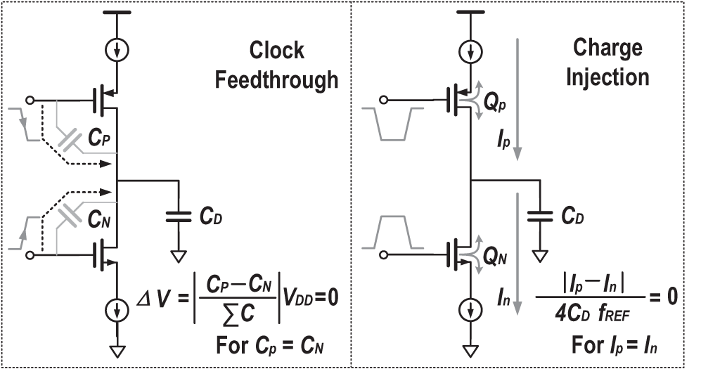
The QSC-PD also benefits from the sharp transfer characteristic of its push–pull structure [Reference Yang, Chen, Yang, Mak and Martins2], which results in a large PD gain (K PD). This effectively suppresses in-band detector noise. Distortion caused by ON-resistance variations of sampling switches is mitigated by complementary device design, which also cancels clock feedthrough. Thus, unlike prior sample-and-hold circuits [Reference Wu, Yao, Godbole, Ni, Chiang, Han, Zuo, Verma, Lu, Son and Cho18], the QSC-PD operates reliably under standard voltage supplies without level shifting. Proper transistor sizing ensures both charge injection and clock feedthrough are simultaneously compensated, as shown in Fig. 10. Although larger CD values further suppress mismatch-induced effects, they introduce a pole that must remain at least hundredfold of fBW to preserve stability. Static phase offsets may arise from OA mismatches or leakage currents in the VCO, requiring the PD to establish a compensating phase shift.
Canceling of clock feedthrough and charge injection by the QSC-PD.

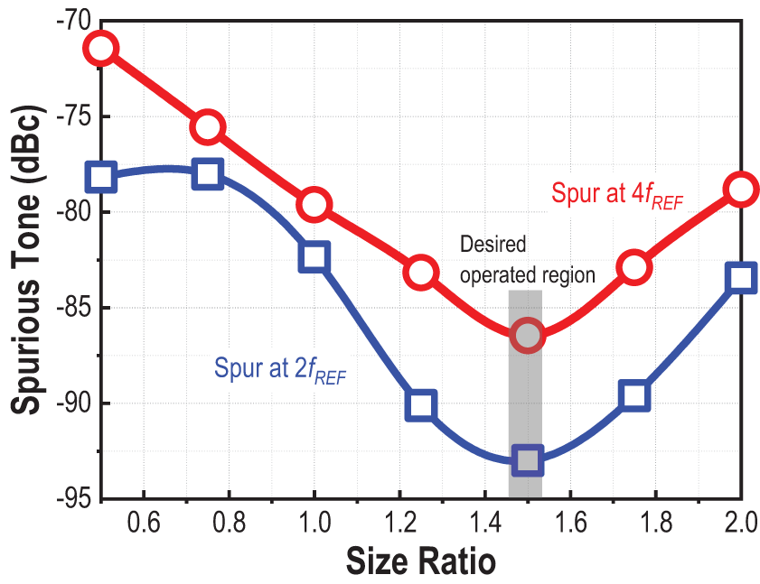
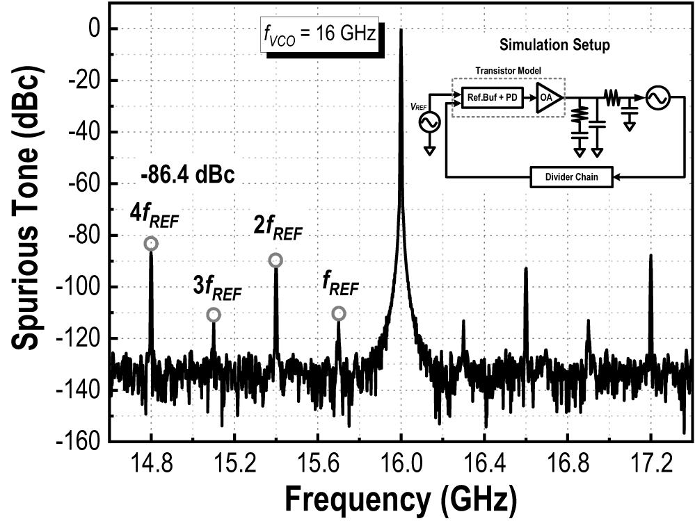
The QSC-PD generates spurs primarily at f REF, 2f REF, and 4f REF. The spur at f REF is typically minimal and originates from parasitic couplings in the OA. Spurious at 2f REF are inherently canceled by the quadrature operation, while those at 4f REF are attenuated by the PLL LPF. Figure 11 illustrates that balanced sizing between PMOS and NMOS devices achieves optimal spur cancellation when the size ratio is ∼1.5.
Simulated spurious tone level against the PMOS-to-NMOS size ratio.

Complete phase-detection path
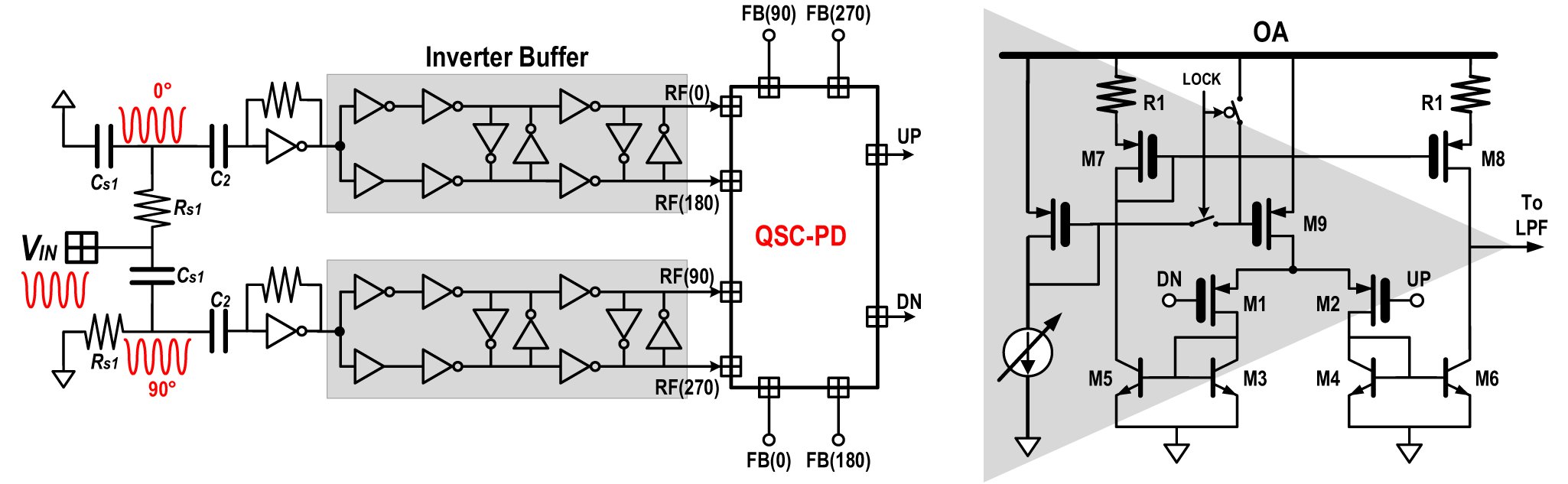
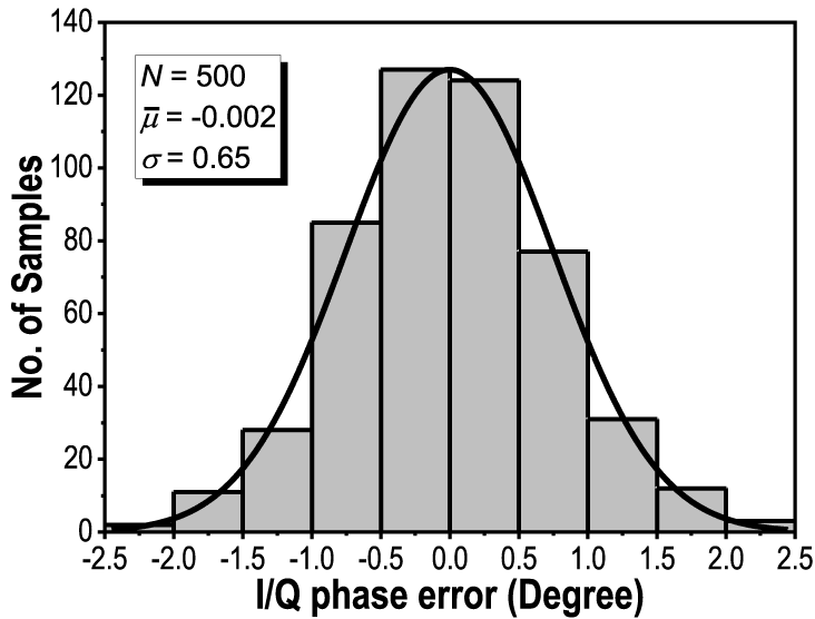
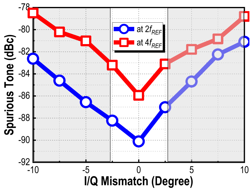
The complete phase-detection path is sketched in Fig. 12 at the next page, including the OA schematic. It integrates an RC-CR network, a reference buffer, the QSC-PD, and the OA. The RC-CR network, which is a polyphase filter, generates quadrature reference signals, though it introduces amplitude and phase imbalance. Monte Carlo analysis shows quadrature phase error within ±2.5°, as summarized in Fig. 13. Simulation of the PLL output shown in Fig. 14 confirms spurious cancellation effectiveness, with the strongest spurious tone at f VCO ± 4f REF measured at −85.6 dBc. As evaluated in Fig. 15, even with I/Q imbalance, spurious tone levels remain below −82 dBc, eliminating the need for calibration.
Full schematic of the phase detection path and the OA.

Monte Carlo statistic of the reference I/Q generator.

Simulated spectrum and spurious tone of the PLL.

Simulated spurious tone against the I/Q mismatch.

When the divider output frequency is sufficiently close to the reference frequency, all harmonics of the beating frequency Δf = |f REF − f DIV| are cancelled by the QSC-PD, leaving only the fundamental tone. It implies that the QSC-PD ultimately generates a near-DC voltage at its output, which gradually modulates the VCO control line voltage and allows the VCO to reach phase-locked. In this manner, the subsequent OA converter can be employed here to convert the above near-DC output voltage to current I OA = Gm × (Vc − VcB), where Gm is the OA transconductance gain and improves the overall PD gain. At phase-locked, Vc − VcB ≈ 0. In this manner, the OA does not need to use the same supply voltage as the QSC-PD: it can instead use a higher voltage for driving the VCO and hereby extends the VCO frequency tuning range. In our implementation, the QSC-PD and the reference buffers adopt 1.2 V supply voltage, while it is 3.3 V for the OA. To ensure such an arrangement, the VCO has to adopt thick-oxide accumulation-mode MOS varactor that can handle 3.3 V voltage.
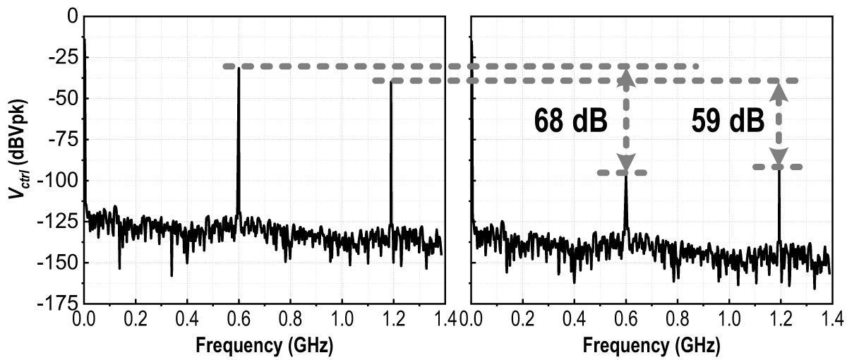
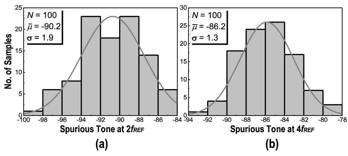
The OA, as shown in Fig. 12, designed with thick-oxide transistors and large dimensions to minimize flicker noise and process variation, is disabled during VCO lock detection to avoid interference between phase detection and lock detection. Compared with the half-topology shown in Fig. 8, ripple suppression at 2f REF and 4f REF exceeds 59 dB, as shown in Fig. 16. Further suppression on the 4f REF harmonic relies on smaller PLL fBW and the corner frequency of the LPF, both of which may degrade the level attenuation to the VCO phase noise. Moreover, Monte Carlo simulations (Fig. 17) confirm consistent spurious tone suppression across process variations.
Simulated VCO control line voltage ripple amplitude.

Statistics of the spurious tone evaluated at (a) f vco − 2f REF and at (b) f vco − 4f REF.

PD phase noise consideration
To ensure that the overall phase noise of the phase detection path is lower than that the reference signal, the QSC-PD phase noise must be sufficiently suppressed near the PLL loop bandwidth. With properly sized devices (PMOS switches: 22 µm/150 nm, NMOS switches: 18 µm/150 nm, converters: 26 µm/220 nm), the QSC-PD achieves a phase noise of −158.5 dBc/Hz at 6 MHz offset frequency and burning 967 µW power. The large OA input devices and source degeneration further suppress flicker noise. Overall, when scaled by divider ratio N, the complete QSC-PD contributes −122.7 dBc/Hz evaluated at 1 MHz frequency offset, approximately 5 dB lower than the reference noise level. This leaves sufficiently noise margin for the entire phase detection path. Increasing the static current for the QSC-PD and the OA can lower their intrinsic noise.
VCO lock detection
Implied by (2), the QSC-PD leverages beat frequency detection to enable fast acquisition. The QSC-PD produces a baseband component proportional to |f vco/N − f REF|, strongly modulating the VCO until the PLL locks. Simulations confirm a capture range exceeding the tuning span of individual VCO bands, thus eliminating the need for auxiliary FLLs.
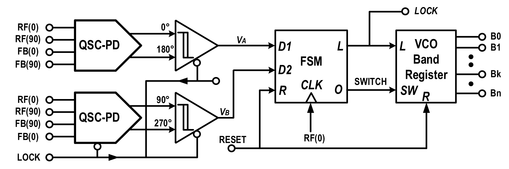
The high detector gain also allows reducing K VCO while maintaining loop gain, easing design for wideband mm-wave PLLs. Lock detection exploits the beat signal (fB = |f DIV − f REF|) using Schmitt triggers to filter glitches and produce reliable logic levels. As shown in Fig. 18, this enables robust VCO band selection.
Circuit realization of the VCO lock detector exploiting a pair of QSC-PD for frequency detection.

The VCO lock detection scheme integrates two QSC-PDs, Schmitt triggers, and a finite-state machine (FSM) for lock detection. The tolerable beat frequency range by each QSC-PD, which is at least 2 GHz for a power consumption of 1.6 mW, far exceeds any frequency offsets during frequency detection, and thus ensuring reliable operation across process variation. The frequency detection is performed by continuous sampling of the voltage VA of the first QSC-PD output by the voltage VB at the second QSC-PD output, utilizing a D flip-flop. The sampled results indicate whether the frequency divider output frequency is faster or slower, compared with the reference frequency. The sampled voltage feeds to the FSM for processing in the digital domain. The FSM aims to gradually eliminate the frequency error by continuously switching the VCO band. The lock detection process systematically increments VCO bands until the correct frequency range is reached. This method achieves microsecond-scale lock detection without reliance on loop components, outperforming conventional approach exploiting voltage-based comparators.
PLL and mm-wave components
Voltage-controlled oscillator
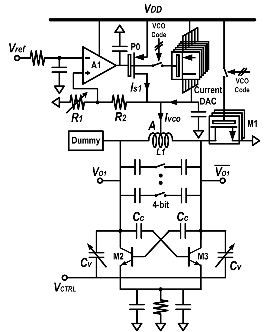
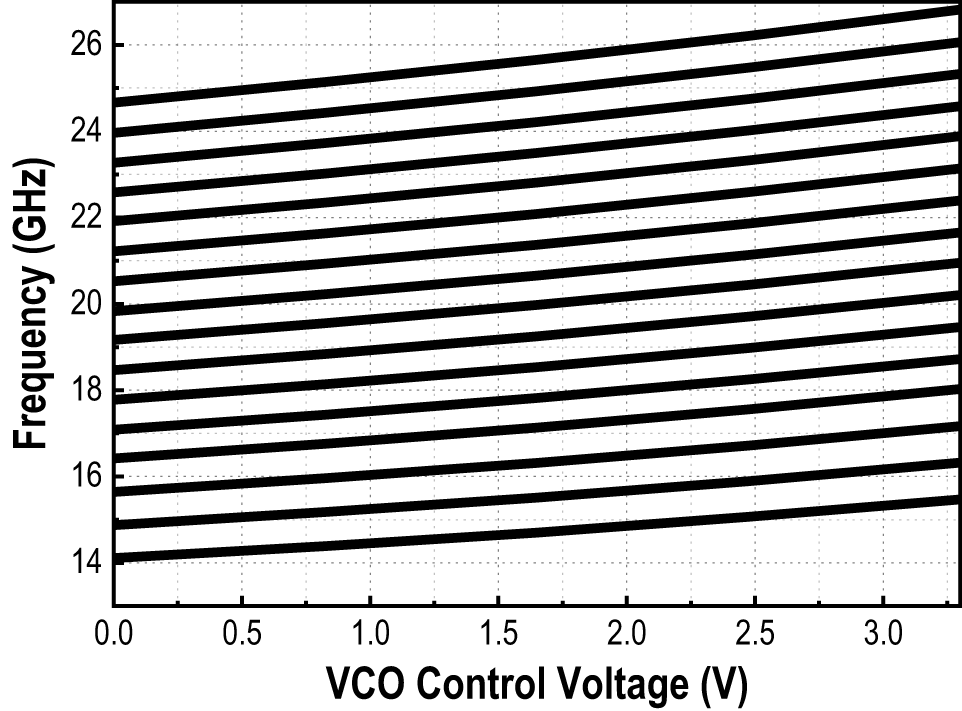
A wideband and low-phase-noise class-C LC VCO with a voltage regulator is adopted, as shown in Fig. 19. The voltage regulator, realized by error amplifier A1, power MOSFET P0, and feedback resistor R 1 and R 2, compensates for supply fluctuations, achieving a power-supply-rejection-ratio of 47 dB at 1 MHz. R 1 and R 2 also define the supply voltage for the VCO to prevent the VCO from entering breakdown region. The VCO tuning range extends from 14 to 26.8 GHz, with fine frequency tuning provided by thick-oxide accumulated-mode MOS varactors. Coarse frequency tuning is achieved through a 4-bit capacitor bank, and the automatic frequency control (AFC) is governed by the LD described in Section III. A current DAC, digitally set by the LD, ensures consistent oscillation swing across frequency bands, which is essential to ensure that the prescaler can always lock to the VCO output frequency within the entire operating range.
Millimeter-wave SiGe BiCMOS class-C VCO.

The phase noise optimization of the SiGe bipolar complementary metal oxide semiconductor (BiCMOS) class-C VCO can be found in paper [Reference Garghetti, Quadrelli, Bassi and Mazzanti24]. Co-design of the VCO and the voltage regulator aims to allow the overall phase noise to be dominated by the base resistance of the VCO. This requires the transistor sizes of the OA in the regulator to be large enough to lower the devices flicker noise. Miller compensator is thus necessary to compensate for the second dominant pole in the OA, to ensure that the voltage regulator is always stable when considering PVT variations.
Inductorless prescaler
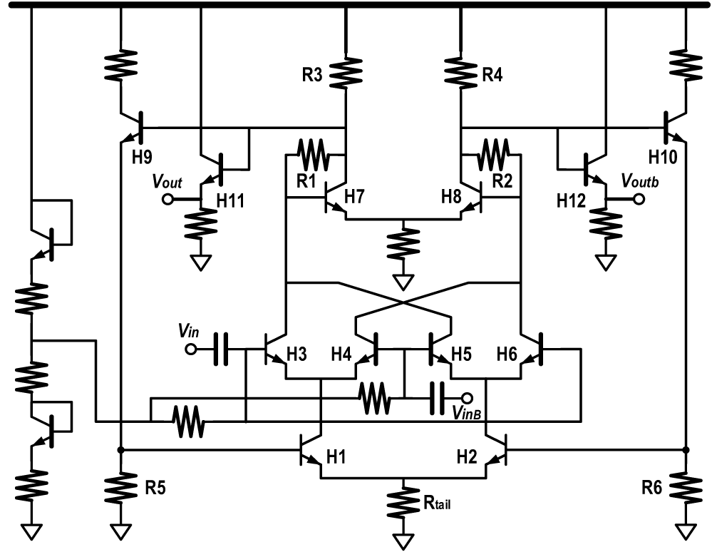
An inductorless divider utilizing a harmonic mixer implemented with HBT transistors H1–H12 is used as the mm-wave prescaler, as shown in Fig. 20. The harmonic mixer is constructed by H1 and H6, while H7 and H8 constitute a low-pass filtered transimpedance amplifier (TIA). The TIA converts the harmonic current from the mixer to voltage and drives the following common-emitter buffer realized by H11 and H12. Denotes the input differential signal (V in and V inb) with a frequency of f in drives the mixing core H3–H6, the common-emitter buffer feeds back signals with a frequency of fi n/2 to the mixer input and again mixes with the input signal to generate f in/2 and its harmonics. To ensure robust divide-by-2 operation, harmonics of f in/2 generated by the mixer must be sufficiently attenuated. As such, the TIA adopts only resistor at the loads without using peaking inductors.
Inductorless prescaler based on harmonic mixer.

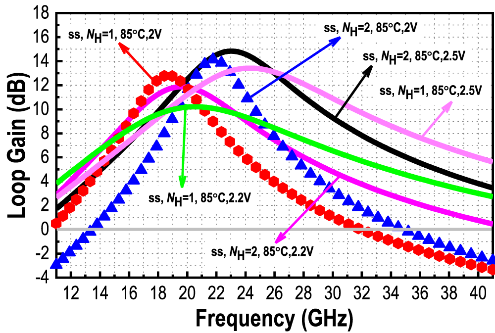
The prescaler’s locking range is essential for covering the full VCO FTR considering possible process variations. The locking range can be evaluated with analysis on its loop gain. By cutting the feedback loop and applying a sinusoidal input at f in/2 to H1 and H2, the loop gain can be measured by the input-to-output frequency response. The achievable locking range, which is 2X of the mixer open-loop UGB (i.e., unity-gain bandwidth), can be estimated by the PAC simulation shown in Fig. 21. The simulation is conducted considering PVT variation. Parameter NH represents the number of identical HBT in parallel. The smallest locking range, observed in the slow–slow corner at NH = 1, 85°C, and VDD = 2 V, spans from 14 to 35 GHz without using an inductor – not sufficient wide to cover the entire VCO FTR considering possible process variation and temperature drift. As such, VDD is at least 2.2 V to gain a higher margin for the locking range. At lower frequencies, frequency division fails because the third harmonic (1.5f in) is insufficiently attenuated. With NH = 1 and VDD = 2.2 V, the divider achieves at least 38 GHz bandwidth. Simulation confirms that the locking range is wide enough at other corners.
Summary of the open-loop gain of the inductorless prescaler.

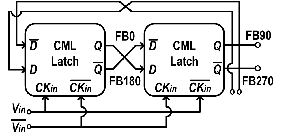
The subsequent divide-by-16 stage employs static dividers, as shown in Fig. 22, and provides quadrature outputs for driving the QSC-PD. Monte Carlo statistic suggests a standard deviation of the I/Q phase error as low as 0.63°. Such a small I/Q phase error leads to a degradation on the PLL reference spur by less than 1 dB.
Static divider generating quadrature signal.

PLL architecture
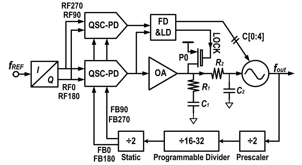
The mm-wave PLL architecture is presented in Fig. 23. It incorporates an input quadrature generator, a pair of QSC-PDs, an OA, an LPF, a VCO, a VCO LD responsible for AFC, and a divider chain. After the VCO band searching (by the LD) is completed, the additional QSC-PD and LD are automatically disabled since they are not responsible for the subsequent phase alignment.
Millimeter-wave PLL architecture.

The LPF consists of a capacitor C 1 and resistor R 1, producing a zero to cancel the OA’s phase lag. No other capacitor is required for the PLL loop as the QSC-PD already introduces a pole constituted by CD and its ON-resistance. Additional RC network C 2 and R 2 further suppress the high-frequency spurious tone further. The pole frequency is at least hundredfold of the PLL loop bandwidth, imposing negligible impact to the PLL stability.
Experimental results
The mm-wave PLL was implemented in a commercial 130-nm SiGe BiCMOS process, with the die micrograph and power breakdown provided in Fig. 24. The active chip area is 0.7 mm2. Phase noise and spectrum measurements were performed with an R&S FSUP26 phase noise analyzer, while the reference signal was generated by R&S SMF100A signal generator. The PLL power consumption is 39.6–44.5 mW. As the FD and LD are turned off right after the VCO finalized its AFC, their power consumptions have been excluded. In addition, the power consumption of the mm-wave output driver is excluded as well, since it served only for the testing purpose.
Die photo and power breakdown of the mm-wave PLL.

The VCO frequency tuning range is measured in Fig. 25, indicating an FTR from 14.1 to 26.8 GHz. During the individual VCO test, loop elements such as dividers, the QSC-PD and the OA were disabled, and the control voltage was applied directly through capacitor C 1 in Fig. 23.
Measured free-run VCO tuning curve.

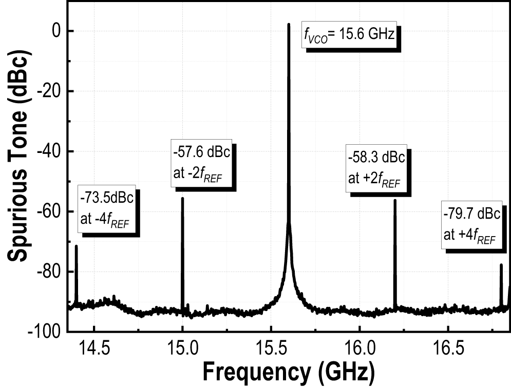
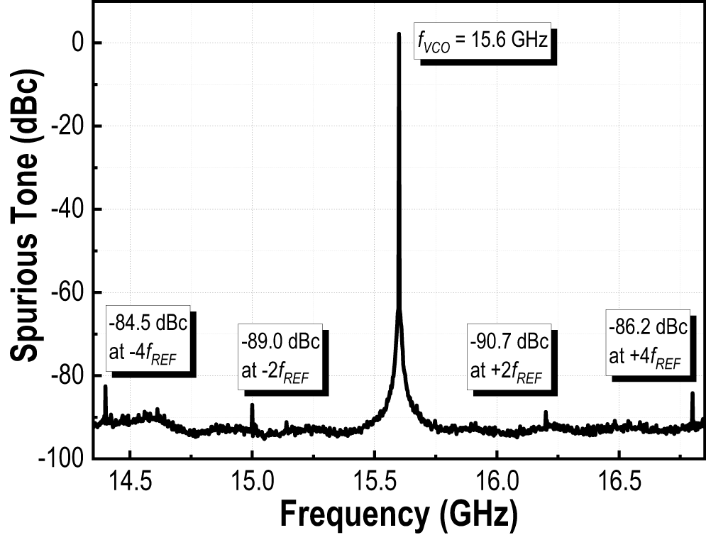
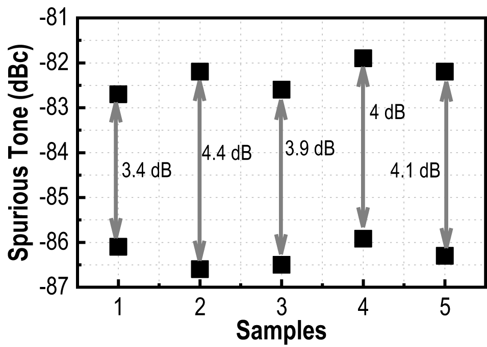
As a direct illustration of the effect of the proposed spurious tone canceling, Figs. 26 and 27 provided the measured PLL output spectrum when half of the QSC-PD and the complete QSC-PD were employed, respectively. The testing was performed at the VCO output at 15.6 GHz. For the case when half of the QSC-PD was employed, the spurious tone level was as high as −57.6 dBc found at f vco − 2f REF, due to strong periodic perturbation on the VCO control line. However, with the spurious tone canceling, the suppression was 11 and 31.4 dB, respectively, at f vco − 4f REF and f vco − 2f REF, with similar level of suppression at f vco + 2f REF and f vco + 4f REF. The highest spurious tone was −84.5 dBc at f vco − 4f REF, indicating more than 30 dB improvement to the reference spur thanks to the QSC-PD, and the dominant spur frequency has been shifted from f vco − 2f REF to f vco − 4f REF. The above comparison confirms the capability of attenuation to the spurious tone by the QSC-PD. Figure 28 summarizes the measured spurious tone across the entire operating range. The largest spurious tone was −81.9 dBc, and the variation was smaller than 4.4 dB collected for five chips.
Measured PLL spectrum with half of the QSC-PD.

Measured PLL spectrum with the QSC-PD.

Summary of measured PLL spurious tone within the PLL operation range.

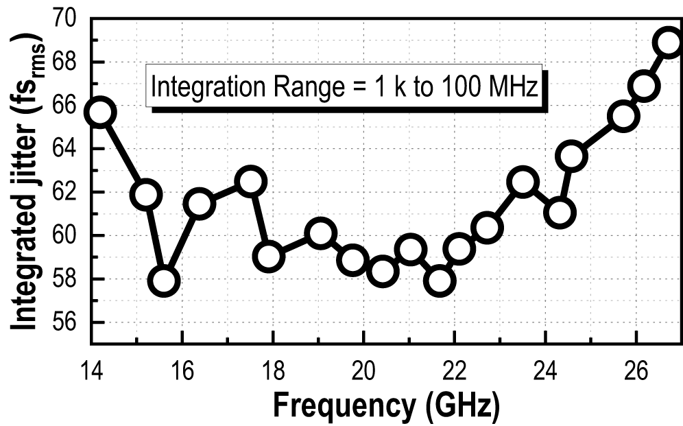
For phase noise measurements, the external voltage supply was removed from capacitor C 1 to prevent interference with the control node. At 15.6 GHz, the PLL exhibited −112.3 dBc/Hz at 10 kHz offset and −112 dBc/Hz at 1 MHz offset, as shown in Fig. 29. The integrated jitter from 1 kHz to 300 MHz was 57.9 fsrms. Noise decomposition showed that the reference buffer contributed ∼15.2% of the PD noise, dominated by OA flicker noise, and that the in-band PD noise was ∼7.2 dB below the reference noise near fBW. Integrated jitter was limited by the VCO and the reference clock, both of which accounted for ∼40% each of the total jitter. Figure 30 provides the measured RMS jitter (0.001–300 MHz) within the VCO FTR. Integrated jitter smaller than 69 fsrms was observed.
Measured mm-wave PLL phase noise at the VCO output (15.6 GHz).

Summary of measured PLL integrated jitter.

Table 1 benchmarks the proposed design against prior mm-wave PLLs. The prototype achieves the lowest spurious tone level of −84.5 dBc, at least 4 dB better than other reported works. The reported phase noise performance, including integrated jitter and FoMJ, ranks the lowest among recent silicon-based implementations.
Silicon-based millimeter-wave PLLs performance comparison

Note: aFoMJ = 10log10[ $\sigma _{{\text{rms}}}^{\text{2}}$ × Power/1 mW] [Reference Zhao, Forghani and Razavi25].
Conclusion
This paper introduces a QSC-PD for suppressing spurious tones in integer-N PLLs. By incorporating an auxiliary spurious-tone-canceling path, the introduced approach avoids the traditional trade-offs between PLL loop bandwidth and VCO noise suppression while achieving over 30 dB spurious tone rejection. The second branch reuses the current of the primary branch, maintaining the same power while enabling both frequency detection and VCO lock detection. Realized in 130 nm SiGe BiCMOS process, the mm-wave integer-N PLL demonstrates a spurious tone of −84.5 dBc, a minimum integrated jitter of 57.9 fsrms (measured over 1 kHz–300 MHz), and compelling jitter-power FoM of −249 dB (FoM). These results highlight the feasibility of the introduced PLL for emerging high-performance mm-wave–integrated transceivers.
Acknowledgements
This research is supported in part by Guangdong Basic and Applied Basic Research Foundation (2024A1515010236), in part by the Open Project Program of Shanxi Key Laboratory of Advanced Semiconductor Optoelectronic Devices and Integrated Systems under Grant 2024SZKF06, in part by Guangzhou Science and Technology Plan Project (2024A03J0326 and 2024A04J3454), in part by Tertiary Education Scientific research project of Guangzhou Municipal Education Bureau (2024312267), and in part by Key Projects of New Generation Electronic Information (2025ZDZX1022).
Competing interests
The authors declare that they have no known competing financial interests or personal relationships that could have appeared to influence the work reported in this paper.