I. BACKGROUND
A. Justification
With the continued exponential growth of fabrication facility and exposure tool costs,Reference Brown1–Reference Levinson3 the current nanoelectronics fabrication paradigm may not be sustainable.Reference Ross4, Reference Kanellos5 By 2004, the semiconductor lithographic community perceived a rapidly approaching “red brick wall” that has been called the lithographic “triangle of death.” This term refers to the apparent trade-off in conventional top-down lithography between three critical and interdependent chemically amplified resist performance factors, i.e., resolution, throughput, and line edge roughness. The Z-parameter is one of several useful metrics for quantifying the trade-offs among LER, resolution, and dose,Reference Wallow, Higgins, Brainard, Petrillo, Montgomery, Koay, . Denbeaux, Wood and Wei6–Reference Bristol10 as it appears to be relatively constant for a given exposure tool and illumination system. Z is defined, such that:

In 2007, various patterning options, such as: double exposure, double patterning, and spacer double patterningReference Wallow, Higgins, Brainard, Petrillo, Montgomery, Koay, . Denbeaux, Wood and Wei6; lithography-friendly design rules; and model-based OPC corrections were projected to be necessary techniques to achieve the projected CD and dimensional variability requirements at and beyond the 32 nm dynamic random access memory (DRAM) ½ pitch technology node (2013).11 However, these techniques add significant complexity and cost to the lithographic process. They also make it more difficult to achieve the required overlay targets. At the same time, chemically amplified resists appeared to be approaching their respective resolution and dimensional control limits of ~30 nm half pitch, due to acid diffusion, and line width roughness limits of ~4.5 nm (3σ).11
Today, the list of difficult lithography challenges continues to grow. In 2009, the International Technology Roadmap for Semiconductors (ITRS) Lithography International Technology Working Group (ITWG) identified the following among its most difficult challenges: <2.8 nm (3σ) overlay; high-sensitivity resists, with <22 nm ½ pitch resolution; low defectivity, i.e., <0.01 10 nm particles/cm2; and <1.3 nm (3σ) line width roughness.12 In fact, the 2009 revision of the of the ITRS Lithography Exposure Tool Potential Solutions roadmap states the Lithography ITWG’s consensus that there exists “No proven optical solution beyond the 22 nm node.”12 However, since 2007, this Working Group also identified directed self-assembly as a potential patterning solution for the 16 nm DRAM ½ pitch node and beyond.12–Reference Xiao, Cho, Liu and Lee16
B. Definitions
Self-assembly is the process by which atoms, molecules, and/or components spontaneously organize into more complex objects, shapes, and systems. As this term implies, much of the information that drives the assembly of atoms into crystals and the folding of molecules into their secondary and tertiary structures is contained within the each molecule. Directed self-assembly may be seen as an extension of self-assembly, since it leverages the influence of local external factors in addition to self aggregating processes at the atomic, molecular and/or component levels. Specifically, directed self-assembly is the process by which external factors, such as physical templates and/or fields, influence self-assembling systems in desired ways. Template-directed self-assembly typically uses either chemical or topographical patterns to guide the material assembly process. The chemical templating of block copolymers on lithographically patterned monolayers is sometimes referred to as epitaxial self-assembly.17 For example, chemical modification of a substrate surface into hydrophobic and hydrophilic patterns can induce a diblock copolymer to phase segregate into similar patterns.Reference Kim, Park and Hinsberg18 The use of a topographical template to guide the self-assembly process is referred to as graphoepitaxy.Reference Segalman, Yokoyama and Kramer19 Field-directed assembly uses external fields to influence the orientation, formation, and/or growth of self-assembled nanostructures and components.Reference Schaffer, Thurn-Albrecht, Russell and Steiner20, Reference Mayer, Li, Kim, Hu, Morrow, Nimmatoori, Cao, Redwing, Mallouk and Keating21 Examples of useful external fields include: electric, thermal, substrate surface energy, pressure, etc. Consider, for example, the sparse sputtering of indium atoms onto a Si(111) surface, which yields seven-atom triangular clusters. The formation of these clusters is guided by the local surface energy minima on the substrate. The pore template or electrochemically induced synthesis of carbon nanotubes, intrananotube molecular capture, and many catalytic processes represent examples of directed assembly at the nanoscopic scale. Protein translation, which corresponds to the network of complex processes that enable a ribosome to build specific sequences of proteins on demand, is a classic example of directed self-assembly at the mesoscopic scale.
C. DSA landscape
Research is underway that explores new paradigms for assembling, patterning, and fabricating nanoscale materials, structures, and components for nanoelectronics. A key goal of this effort is to identify extensible and sustainable high-volume nanopatterning approaches that enable electronic products with enhanced functional density and diversification, at lower cost.Reference Cavin, Zhirnov, Herr, Avila and Hutchby22 To address this challenge, a significant interdisciplinary knowledge base is growing in several emerging areas of nanoscale patterning and assembly, such as: deterministic fabrication,Reference Philip and Stoddart23–Reference Ruess, Pok, Reusch, Butcher, Goh, Oberbeck, Scappucci, Hamilton and Simmons27 biomimetic patterning,Reference Firouzi, Kumar, Bull, Besier, Sieger, Huo, Walker, Zasadzinski, Glinka and Nicol28–Reference Welander, Stuen, Kang, Liu, Solak, de Pablo and Nealey31 supramolecular self-organization,Reference Lehn32–Reference Stoykovich, Muller, Kim, Splak, Edwards, de Pablo and Nealey43 field-directed assembly,Reference Mayer, Li, Kim, Hu, Morrow, Nimmatoori, Cao, Redwing, Mallouk and Keating21, Reference Cavin, Zhirnov, Herr, Avila and Hutchby22, Reference Smith, Nordquist, Jackson, Mayer, Martin, Mbindyo and Mallouk44–Reference Morrow, Li, Kim, Mayer and Keating47 probe-directed assembly, and/or directed self-assembly,Reference Green, Russell, Jerome and Granville48–Reference Hu, Odom and Lieber65 among others. Within this set of candidate methods, directed self-assembly exhibits the most traction for near-term nanoelectronics patterning applications, as a means for augmenting current top-down lithographic processes. Candidate materials for DSA processing tend to be considered for their potential to replace photoresists, as etch barriers. These materials include nanowires and nanotubes,Reference Hu, Odom and Lieber66–Reference Maune, Han, Barish, Bockrath, Goddard, Rothemund and Winfree80 graphene,Reference Tomalia, Naylor and Goddard81–Reference Ouyang, Dai and Guo88 dendrimers,Reference Hawker and Frechet89–Reference Bosman, Vestberg, Heumann, Frechet and Hawker96 phase-segregating block copolymers,Reference Muthukumar, Ober and Thomas97–Reference Rockford, Mansky and Russell99 and functionalized biomaterials, such as DNAReference Heath and Ratner100–Reference Kershner, Bozano, Micheel, Hung, Fornof, Cha, Rettner, Bersani, Frommer, Rothemund and Wallraff105 and peptides.Reference Cha, Stucky, Morse and Deming106–Reference Johnson, Adams and Cameron108 Phase-segregating block copolymers, as the most mature of these materials, exhibit the nearest-term insertion potential. Consequently, this paper provides an update on the status of this rapidly evolving technology as an enabler for the extensible nanopatterning of nanoelectronics devices.
D. Block copolymers—Their beginnings and basic background information
Chemists began to recognize the unusual properties of diblock copolymers (BCPs),Reference Allen, Downer, Hastings, Melville, Molyneux and Urwin109, Reference Urwin110 such as polystyrene–polymethylmethacrylate [PS–PMMA], soon after they were first reported in 1952.Reference Dunn and Melville111 During the following few decades, considerable attention was given to synthesizing new families of BCPs,Reference Orr and Williams112, Reference Galli, Chiellini and Ober113 cataloging their repertoire of expressed behaviors,Reference Ober, Jin and Lenz114 and characterizing and understanding the factors that govern their morphologyReference Balcerzyk, Pstrocki and Wlodarski115–Reference Ross, Chuang and Jung125 and dynamics. Additionally, over the last three decades, a significant body of work has enabled a foundational and predictive knowledge base on the synthesisReference Zhao and Brittain126–Reference Husseman, Malmstrom, McNamara, Mate, Mecerreyes, Genoit, Hedrick, Mansky, Huang, Russell and Hawker132 chemical dynamics,Reference Leibler and Pincus133–Reference Chen and White140 physics,Reference Segalman, Yokoyama and Kramer19, Reference Zhu, Cheng, Calhoun, Ge, Quirk, Thomas, Hsiao, Yeh and Lotz141–Reference Mansky, Liu, Huang, Russell and Hawker153 and patterningReference Mansky, Chaikin and Thomas154–Reference Park, Harrison, Chaikin, Register and Adamson159 of thin film block copolymeric systems. Today, living free radical polymerization provides a robust synthetic route to achieving designed and useful block copolymers, such as PS–PMMA.
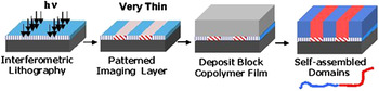
“A successful directed self-assembly technology requires control of three interdependent factors: A material assembly instruction set, an internal assembly tool box, and a set of processes that guide how a given material interacts with its local environment. For example, consider the directed epitaxial self-assembly of block copolymers on lithographically defined nanopatterned substrates. A copolymer is any polymer that is built from more than one monomer type. The family of copolymers made from two monomer types, A and B, can exist as one of three forms: random, alternating, or block. A random copolymer is characterized by a random ordering of the A and B monomer units in the polymeric chain, such as BBABAAABAABBBAB. Alternating copolymers exhibit a regular alternating pattern of monomer units in the polymeric chain, such as ABABABABABAB. Block copolymers represent an unusual class of polymers that are synthesized from two or more distinct homogeneous polymeric blocks. For the case of a diblock copolymer, the structure might correspond to AAAAAAAAAAA–BBBBBBBBB and is represented by the blue and red sections of the polymer chain shown in the last frame of Fig. 1. Each block is homogeneous and may exhibit similar or dissimilar, oil-like (blue) versus water-like (red), behaviors. It is this latter property that exhibits significant potential for sublithographic patterning.
Epitaxial self-assembly of block copolymers on lithographically defined nanopatterned substrates. Graphic courtesy of the research group of Paul Nealey, University of Wisconsin-Madison, used with permission.

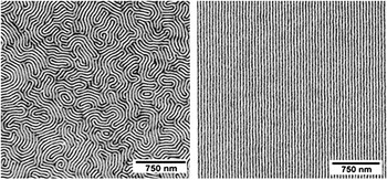
A diblock copolymer contains information that determines its preferred mode of assembly into a film. It codes for whether the blocks will remain miscible or tend to phase segregate into sheets, lamellae, embedded rods or cylinders, or embedded spheres. Each block also codes for the dimensions of the preferred phase-segregated structures, preferred orientation with respect to the local external environment, and other useful macroscopic properties. Hence, a diblock copolymer contains a rudimentary internal instruction set that influences its internal assembly options. Without additional information or factors to guide the assembly process, a phase-segregating diblock copolymer film on a bare substrate might generate rather random patterns of block specific domains, similar to the spaghettilike strings of symmetric poly(styrene-b-methylmethacrylate) shown in Fig. 2(a).
Phase-segregated film of symmetric poly(styrene–b-methylmethacrylate), Lo ≈ 48 nm, on: (a) an unpatterned surface and (b) a patterned surface, for which Ls = Lo. The long-range homogeneous ordering in image (b) was achieved by lithographically templated self-assembly. Photographs courtesy of the research group of Paul Nealey, University of Wisconsin-Madison, used with permission.

However, we also can use the interaction of this block copolymer with its local environment to constrain and guide the polymer film’s growth and assembly process. For example, one might lithographically activate desired regions of a substrate, as shown schematically in the first two frames of Fig. 2. This process creates mileposts or markers that give further guidance to the block copolymer on how it should assemble. Suppose the lithographic step converts a nonpolar, oil-like, surface to a more polar, water-like, domain of monolayer thickness. This could be as simple as converting a hydrogen-terminated silicon surface to hydroxyl-terminated regions, selectively binding molecular brushes, or modifying the surface topography, such as by forming a shallow trench. This local external environment will influence and direct how the deposited block copolymer film will self-assemble on these surface differentiated domains. This is shown schematically in the last step of Fig. 2, below.
Will top-down lithography give way to bottoms-up self-assembly? It is more likely that a more hybrid approach, such as directed self-assembly, will augment and extend the capabilities of the top-down technology of choice. For directed self-assembly technology to succeed, it is not sufficient to direct the assembly of patterns with top-down lithographic resolution. Surface activation, through the chemical patterning of polymeric brushes, offers a near ideal thickness to minimize depth of focus issues in the patterning process. A lithographically patterned monolayer minimizes depth of focus requirements for the surface patterned features. When a thin block copolymer film is deposited on this chemically patterned surface and annealed, the high-fidelity chemical template facilitates phase segregation into desired nanostructures. However, top-down patterning does little to extend scaling. The internal coding and assembly dynamics of imaging materials, such as block copolymers, offer an additional set of tools for enhancing the resolution and dimensional control of a conventional patterning process. It is the combined top-down and bottom-up approach that may extend the feasibility and affordability of optical lithography by several technology nodes.
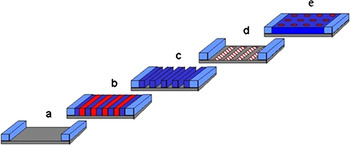
Can directed self-assembly achieve sublithographic resolution? Yes, but it may require more unit process steps than a conventional lithographic technology. Consider the graphoepitaxially directed self-assembly process shown in Fig. 3. This process begins with top-down patterning, such as via optical lithography, which topographically activates desired regions on a substrate surface. This step defines gross features, within which desired sublithographic order will be achieved. For example, coating this constrained activated region with an appropriately encoded block copolymer could induce phase segregation and directed self-assembly of the lamellae-forming block copolymer. Furthermore, one block can be selectively removed and the exposed regions of the substrate selectively activated. This step transfers sublithographic information to the substrate surface that enables the formation of a second pattern at higher resolution. Coating this dual-activated and constrained surface region with another well-designed copolymer might enable the directed self-assembly of well-ordered periodic arrays of embedded rodlike structures, orthogonal to the substrate surface. These cylindrical structures would exhibit sublithographic lateral dimensions. Potential near-term applications could include the fabrication of magnetic hard drives with ~10 nm pixel resolution.
Summary of the graphoepitaxial process for achieving regular arrays of sublithographic structures, with long range, that includes: (a) A chemically and/or topographically patterned substrate, (b) directed self-assembly of lamellae-forming block copolymer, (c) selective removal of one block, (d) pattern transfer to imaging layer, creating a second pattern at higher resolution, and (e) directed assembly of cylinder-forming block copolymer. Graphic courtesy of the research group of Paul Nealey, University of Wisconsin–Madison, used with permission.

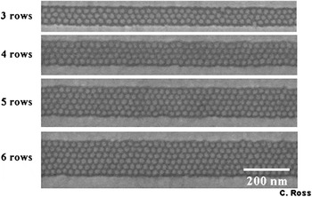
The following example demonstrates the feasibility of applying lithographically templated graphoepitaxy to induce short- and long-range order in phase-segregated embedded spherical or columnar structures. E-beam or 193 nm optical interference lithography was used to create surface-activated domains of 40 nm trenches, of varying pitch, with current minimum achievable periods down to ~100 nm. This constrained surface region induced a polystyrene–polyferrocenyldimethylsilane (PS–PFS) diblock copolymer to self-assemble into a thin film of closely packed structures with short- and long-range order, shown in Fig. 4. The spacing and diameter of the phase-segregated dots appear to be rather uniform, ~20 nm, over the entire field of view. The number of rows of dots is determined by the size and nature of the unit blocks in the copolymer and the dimensions of the lithographically templated surface region. This result is encouraging and suggests the feasibility of using directed self-assembly to pattern well-ordered patterns of deep nanoscale features”.Reference Herr159a
Lithographically templated assembly of a polystyrene–polyferrocenyldimethylsilane (PS–PFS) diblock copolymer into a regular array of close packed structures, exhibiting short- and long-range order. Photographs courtesy of the research group of Ross and Chuang, Massachusetts Institute of Technology, adapted from Cheng, Nature Materials, 3(11), 824 (2004), used with permission.

For additional information, readers are referred to several recent papers that provide good overviews of additional background and BCP-directed self-assembly related information.Reference Darling160, Reference Kim, Park and Hinsberg18
II. PROJECTED NANOELECTRONICS PATTERNING REQUIREMENTS
“If DSA is to be considered a viable and competitive patterning option, it must be able to form a desired set of structures at dimensions at least a factor of 2 smaller and with twice the density as can be achieved by conventional lithographic methods. This corresponds to resolution and line edge roughness (LER) targets of <12 nm and <1.3 nm, respectively. The structures must form in predefined locations with respect to existing structures, and with low defect density. The net time required to form and fix a pattern must be compatible with conventional inline process requirements and a throughput of 120 wafers (300 mm) per hour. Also, the ability to achieve pattern registration, required feature sizes, density, low defect levels, etch resistance, and process times must be demonstrated simultaneously in an experiment with the same material”.17
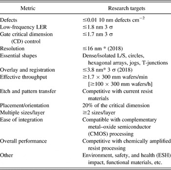
This quote reflects some of the projected DSA performance metrics that are required for this technology to be considered for insertion into a high-volume manufacturing flow. While certain aspects of these systems are beginning to mature within the research community, the BCP family of polymers remains classified as an emerging research material. The current corresponding set of directed self-assembly research targets, which must be satisfied before this technology can be considered for transition to development and insertion into nanoelectronics manufacturing, is shown in Table I. These research targets are based on the 2009 ITRS projected lithography requirements for 2015, i.e., 3 to 4 years before DSA’s earliest potential insertion date. This date was selected to reflect the need for at least 3 years to develop a sufficiently robust supplier infrastructure and set of patterning products.

These research targets will be refined and become more application specific as BCP technology evolves toward a given product. For example, even though the industry is moving toward regular fabrics, the patterning needs of the logic and memory communities will continue to differ, especially with respect to the specific basis set of shapes required by their respective design teams.
III. STATE-OF-THE-ART IN TEMPLATED BLOCK COPOLYMER PATTERNING
This section provides an update on the status of diblock copolymer based directed self-assembly for future nanoelectronics-related applications. Additionally, this update compares the best block copolymer performance, to date, with the research targets defined by the nanoelectronics community, shown in Table I. These targets provide the framework for an ITRS assessment, in 2012–2013, on directed self-assembly’s insertion potential for the 16 nm microprocessor unit (MPU) node, in 2018, and/or the 16 nm DRAM ½ pitch node, in 2019. If the research community finds one or more families of BCPs that satisfy these targets, then they may warrant consideration for commercialization and integration into the manufacturing flow of a future nanoelectronics fabrication facility. However, no block copolymer has been found to satisfy all of the specified research targets.
A. Defect densityReference Craig and Nealey164
Of the metrics listed in Table I, the defect density target may represent this technology’s greatest unknown and greatest challenge. Limited data on chemically patterned substrates suggest that currently reported defect densities, from patterns formed in a university lab, are orders of magnitude greater than the research target of ≤0.01 10 nm defect/cm2.165 However, it should be noted that university labs are not expected to achieve the process and environmental controls of a semiconductor clean room. Studies are scheduled161 to assess the defectivity of BCP-based directed self-assembly in a more manufacturing-like environment by early 2011.
What drives defect formation? Will defect density limit DSA’s insertion into high volume semiconductor manufacturing? What are the limits of defect free pattern density multiplication; i.e., when does defect formation become energetically favored? For nanostructures that form through the phase segregation of block copolymers, equilibrium defects are relatively few and largely originate from kinetic effects arising during film growth or from the confinement of these materials, when they are topographically directed. At any temperature, there will be an equilibrium concentration of defects governed by a Boltzmann distribution. When required pattern formation anneal times exceed experimental limitations, then material mass transport is extremely slow and kinetically induced defects may be effectively “frozen” into the system.165–Reference Hammond, Cochran, Fredrickson and Kramer167 Several numerical techniques, such as spectral amplitude filtering and force-biased, partial saddle point Monte Carlo algorithms have proven useful for removing metastable defects in block copolymer thin film simulations and for potentially examining equilibrium defect populations.Reference Bosse, Sides, Katsov, Garcia-Cervera and Fredrickson168 Such predictive tools may assist with the design and optimization of high-performance copolymeric systems.
B. Low-frequency LER,Reference Stoykovich, Daoulas, Muller, Kang, De Pablo and Nealey162 gate CD control, and resolution
Notwithstanding the lack of defect data, progress has been made in several key areas.Reference Stoykovich, Daoulas, Muller, Kang, De Pablo and Nealey162, Reference Nealey, Bowling, Capodieci, Eib, Herr, Robertson and Zhirnov169–Reference Liu, Thomas, Craig and Nealey172 For example, a recent paper reports LER measurements of 1.95 nm (3σ)Reference Stoykovich, Daoulas, Muller, Kang, De Pablo and Nealey162, Reference Edwards, Muller, Stoykovich, Solak, de Pablo and Nealey170, Reference Stoykovich, Kang, de Pablo and Nealey171, Reference Liu, Han, Ji, Detcheverry, de Pabo, Gopalan and Nealey173, Reference Liu, Chang, Raub, Yoshida, Wallow, Han, Kang, Gopalan, Brueck, Ma and Nealey174 for 16 nm PS features, formed using PS–b-PMMA. The observed edge smoothing appears to be driven by the interfacial energy of the phase-segregated domains, which reflects the interblock repulsion.
PS–b-PMMA systems typically achieve domain diameters ranging from ~10 to 80 nm, with long-range PS domain width variability reported to be as low as ~1 nm.Reference Stoykovich, Daoulas, Muller, Kang, De Pablo and Nealey162, Reference Edwards, Muller, Stoykovich, Solak, de Pablo and Nealey170, Reference Stoykovich, Kang, de Pablo and Nealey171, Reference Edwards175 Such a low-magnitude long-range CD variation reflects the self-healing properties of chemically patterned BCP systems, which tend to smooth out much of the lithographically induced template edge variability. Phase-segregating BCPs also exhibit the potential for chemical proximity correction, which refers to the ability to design and tune block polymer parameters to achieve desired features, critical dimensions, and functionality.Reference Event176
Critical factors that impact resolution include the interaction parameter, χ, polymer-solvent interactions, and feature density multiplication. Increasing χ has yielded sub-10 domain diameters. For example, models suggest that sub-5 nm spherical and lamellar morphologies should be possible with a hydrogenated polyisoprene–polylactide (HPI–PL) block copolymer.Reference Event176, Reference Zhao, Feng, Huo and Melosh177 The feasibility of resolving arrays of extremely small domains has been experimentally validated. Mesoporous silicate films, formed from the infusion of a silicate into a phase-segregated BCP matrix, exhibit some of the smallest domain sizes reported to date, i.e., with pore diameters of ~3 nm.Reference Yang, Zhoa, Margolese, Chmelka and Stucky178–Reference Nagarajan, Russell and Watkins183 Some of these well-ordered, low-κ dielectric arrays are enabled by host matrices comprising BCPs, such as polystyrene–b-p-tert-butyloxycarbonyloxystyrene (PS–b-PtbocST), poly(ethylene oxide)–poly(propylene oxide) (PEO–PPO), and (poly(ethylene oxide)–b-poly(propylene oxide)–b-poly(ethylene oxide)) or Pluronic block copolymer templates (PEO–b-PPO–b-PEO).
C. Essential shapesReference Stoykovich, Muller, Kim, Splak, Edwards, de Pablo and Nealey43, Reference Stoykovich, Kang, Ch. Daoulas, Liu, Liu, de Pablo, Muller and Nealey184
DSA has demonstrated the feasibility of achieving many of the shapes required by the design community, including dense and isolated lines and spaces, dense arrays of holes, T-junctions, and jogs.Reference Stoykovich, Muller, Kim, Splak, Edwards, de Pablo and Nealey43, Reference Nealey185, Reference Park, Kim, Hawker, Kramer, Bang and Ha186, Reference Stoykovich, Kang, Daoulas, Liu, Liu, de Pablo, Muller and Nealey186a The formation of useful structures can be facilitated by the careful blending of BCPs with their corresponding homopolymers. Additionally, considerable progress has been made in understanding how to direct and control domain packing. For example, a graphoepitaxial approach has been used to guide the phase segregation of a polyferrocenyldimethylsilane–polystyrene, PFS–PS, diblock copolymer into arrays of spherical domains. These hexagonally packed domains exhibit long-range order, when the trench width is an integral number of the domain dimensions.Reference Ross187–Reference Ross189 Moreover, by engineering the groove topography, one can achieve ellipsoidal domains and other packing orders, such as a face-centered-cubic lattice with square symmetry (100) at the surface.Reference Ross, Chuang and Jung125 Predictive models are emerging that soon may be sufficient to design more complex and more arbitrary 2D shapes, through chemical patterning.Reference Kang, Craig and Nealey190–Reference Kang, Craig and Nealey192
D. Multiple sizes per layer
Thus far, it has been difficult to achieve multiple pitches within a given templated area. However, it is now becoming possible to selectively control the patterns and morphologies formed within desired areas, in a given layer.Reference Liu, Thomas, Craig and Nealey172, Reference Edwards, Stoykovich, Nealey and Solak193–Reference Cheng, Rettner, Sanders, Kim and Hinsberg195 Specifically, recent studies that combine polymer cross-linking with a solvent anneal have demonstrated multiple morphologies in one layer. For example, the selective cross-linking of PaMS–b-PHOST, after an acetone anneal, can be used to lock in a spherical morphology in desired areas. A subsequent THF anneal can then be used to drive the uncross-linked regions to a cylindrical morphology.Reference Bosworth, Black and Ober196
Additionally, the combination of hybrid lithographyReference Fritze, Bloomstein, Tyrrell, Fedynshyn, Efremow, Hardy, Cann, Lennon, Spector and Rothschild197 and chemical patterning can yield trimmed patterns, with desired BCP geometries.Reference Kang, Craig and Nealey190 Hybrid lithography has been used to trim and guide the assembly of useful surface patterns. Specifically, a checkerboard trim was applied to generate BCP pillar or contact arrays, while a rectangular trim yielded useful DRAM patterns, with different-sized features within the same layer.Reference Stoykovich, Daoulas, Muller, Kang, De Pablo and Nealey162, Reference Edwards, Muller, Stoykovich, Solak, de Pablo and Nealey170, Reference Stoykovich, Kang, de Pablo and Nealey171, Reference Stoykovich, Edwards, Kang, Liu, Welander, Na, Park, Cerrina, de Pablo and Nealey198, Reference Cheng, Rettner, Sanders, Kim and Hinsberg199 Such a hybrid DSA patterning technology may have some benefits over a conventional hybrid lithographic process, which uses conventional resists. Trimming a thin chemical brush layer is less sensitive to depth-of-focus issues than a conventional, and typically thicker, resist layer. Within the trimmed patterns, it also may be possible for BCPs to further assemble into additional and more complex patterns, with sublithographic resolution.200
E. RegistrationReference Black and Bezencenet201 and orientationReference Ruiz, Sandstrom and Black202
In graphoepitaxially guided assembly, programmed defects in the trench sidewallReference Cheng and Ross203 or acute trench corner geometries give clues for registering arrays of phase-segregated domains.Reference Ross, Chuang and Jung125 Positional errors on the order of ~3 nm are reported for domains registered to a trench corner, with an acute 60° angle. This observation suggests that specific substrate features can facilitate domain registration, by pinning the placement of each interdependent domain in the array.
Density multiplication provides another tool for registering higher-density and higher-resolution domains. This technique relies on the interpolation of BCP domains between sparsely patterned markers on the substrate. These markers can be localized chemical patterns, such as brushes, or structural features, such as posts. The interpolated assembly process can significantly reduce the required overhead time for top-down patterning tools, as multiplication factors of 4 or more have been demonstrated for regularReference Edwards, Muller, Stoykovich, Solak, de Pablo and Nealey170, Reference Stoykovich, Kang, de Pablo and Nealey171, Reference Ruiz, Kang, Detcheverry, Dobisz, Kercher, Albrecht, De Pablo and Nealey204, Reference Nealey and Liu205 and complex array shapes.Reference Stoykovich, Daoulas, Muller, Kang, De Pablo and Nealey162, Reference Edwards, Muller, Stoykovich, Solak, de Pablo and Nealey170, Reference Stoykovich, Kang, de Pablo and Nealey171 More recently, the designed patterning of sparse guideposts has enabled the local registration and orientation of nonregular phase-segregated structures.Reference Edwards, Stoykovich, Nealey and Solak193, Reference Yang, Jung, Chang, Mickiewicz, Alexander-Katz, Ross and Berggren206, Reference Kim, Oh, Jung and Ilsin207 These results suggest that there may be a minimum amount of patterned information needed to guide the formation of a specific complex pattern. Considerable work is needed to establish guiding principles for designing the sparsest set of mileposts required for a given arbitrary set of useful laid-out features.
F. Effective throughput
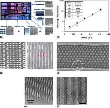
Throughput represents another potential insertion barrier. In the past, typical anneal times for graphoepitaxy, chemical patterning, solvent,Reference Kim, Misner, Kimura and Russell208 and supercritical CO2 ranged from ~0.5 to 3 days.Reference Welander, Stuen, Kang, Liu, Solak, de Pablo and Nealey31, Reference Craig, Kang and Nealey209, Reference Nealey210 For certain functional hybrid BCP systems, anneal times of 4 days are needed to achieve sufficient phase segregation.Reference Zhu, Gambino, Rafailovich, Sokolov, Schwarz and Gomez211 However, it is now understood that polymer mobility drives the phase-segregation process. This means that a 2.0–2.5 h anneal, at 180 °C, can be completed in only 2–3 min at 220 °C, which is within a factor of 4 of the individual wafer research target.Reference Welander, Stuen, Kang, Liu, Solak, de Pablo and Nealey31 If the system could tolerate higher anneal temperatures, then anneal times of 1 min or less would be possibleReference Stoykovich, Daoulas, Muller, Kang, De Pablo and Nealey162, Reference Edwards, Muller, Stoykovich, Solak, de Pablo and Nealey170, Reference Stoykovich, Kang, de Pablo and Nealey171, Reference Welander, Kang, Stuen, Solak, Muller, De Pablo and Nealey212 In fact, anneals at 250 and 280 °C would be complete at 14 and 1.4 s, respectively.Reference Nealey210
Since pattern formation within a block copolymer occurs during a bake step, effective anneal times per wafer can be enhanced by running batch anneals. A 150 s anneal of a 25-wafer batch corresponds to an effective anneal time of 6 s per wafer. By leveraging the benefits of a batch anneal process, even a 15 min wafer anneal time for this 25-wafer batch would satisfy the effective research target for throughput.
G. Etch and pattern transfer, ease of integration, and overall performance
Many of the BCPs considered for patterning applications contain polymeric blocks, such as PS, PMMA, PHOST, etc., that are used in current resist formulations. Consequently, the etch behavior of at least some BCP formulations is expected to be comparable to that of conventional resists. Since the DSA pattern formation process strongly couples with the anneal step, and less directly with the lithographic exposure process, it also may be possible to engineer polymeric blocks with enhanced pattern transfer functionality.
Several teams have demonstrated the feasibility of fabricating functional components, such as capacitors,Reference Black, Guarini, Milkove, Banker, Russell and Tuominen213–Reference Guarini, Black, Zhang, Kim, Sikorski and Babich215 devices,Reference Black216 and air gap structuresReference Johnson217 for interconnect applications using BCP-directed self-assembly. The capacitor application requires patterns that can generate a high surface area, with little need for alignment of the assembled features. However, the device application requires an assembly process that yields features of uniform size, with sufficient dimensional control, order, and registration. An early silicon nanowire-array FET fabrication project used graphoepitaxy to guide the assembly of PS–PMMA lamellar structures, which were selectively transferred into the substrate. While the corresponding device exhibited functionality, the resulting nanowires suffered from edge roughness and dimensional variability.Reference Ross, Chuang and Jung125, Reference Cheng and Ross203, Reference Black216 In fact, the impact of trench-edge variability on BCP domain ordering appears to increase with anneal temperature, which may adversely impact anneal times.Reference Kramer218–Reference Ponoth, Horak, Colburn, Breyta, Huang, Sucharitaves, Landis, Lisi, Liu, Vo, Johnson, Li, Purushothaman, Cohen, Hu, Kim, Clevenger, Fuller, Nogami, Spooner and Edelstein220 With respect to BCP-based air-gap technology, “performance modeling indicates that the expected capacitance gain is 35%, and this was routinely observed by in-line measurements. One advantage of this technology is a lower cost compared to other subtractive air gap schemes.”
Elsewhere, early results suggest that BCP-directed self-assembly, using a chemical patterning process, also can be used to fabricate functional nanowire FETs.Reference Liu, Chang, Raub, Yoshida, Wallow, Han, Kang, Gopalan, Brueck, Ma and Nealey174 However, this study warrants replication in a near manufacturing environment to assess the performance and variability of these devices over large areas. For other thoughtful perspectives on DSA-related integration challenges and opportunities, please see the cited set of papers.Reference Black and Bezencenet201, Reference Black and Bezencenet220a, Reference Hawker and Russell221–Reference Kang and Nealey224
Representative images of demonstrated BCP patterning capabilities are shown in Fig. 5.
Selected best in class block copolymer based directed self-assembly results demonstrated to date, with respect to essential shapes, resolution, registration, and throughput. (a) Design community identified a set of seven essential shapes, of which six have been demonstrated. Photograph courtesy of the research group of Paul Nealey, University of Wisconsin–Madison, used with permission. (b) Demonstrated 2–3 min anneal times, but batch anneals could yield sub-30 s effective anneal times. Photograph courtesy of the research group of Paul Nealey, University of Wisconsin–Madison, used with permission. (c) Additional complex patterns achieved by design. Photograph courtesy of the research group of Caroline Ross, Massachusetts Institute of Technology, adapted from Yang, Nature Nanotechnology, 5(4), 258 and 259, 2010, used with permission. (d) Induced edge defects pin the registration of phase segregated domains to <10 nm. Photograph 5 days courtesy of the research group of Caroline Ross, Massachusetts Institute of Technology, adapted from Cheng, Advanced Materials, 15(19), 1601 (2004), used with permission. (e) Demonstrated arrays of 3 nm pores. Photograph courtesy of the research group of Thomas Russell, University of Massachusetts at Amherst, used with permission. (f) Checkerboard patterns achieved with chemically directed block copolymer assembly. Photograph courtesy of the research group of Paul Nealey, University of Wisconsin–Madison, used with permission.

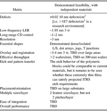
Finally, Table II provides a performance snapshot of current block copolymer based directed self-assembly technology. It should be noted that most of these measurements were made on small wafers or sections of wafers.
Status of key research metrics for BCP-based directed self-assembly.

It is time to leverage ITRS-identified patterning tools and begin to assess the potential of directed self-assembly techniques for their ability to enable the extensible fabrication of sub-16 nm CMOS technology, on 300 mm wafers. Black et al. has already shown that BCPs can generate relatively uniform arrays of phase-segregated patterns over large areas.Reference Guarini, Black, Milkove and Sandstrom225 Currently, at least one project is underway to demonstrate and assess the feasibility of integrating DSA into the manufacturing flow for large-scale wafer applications and to quantify the corresponding process capability and associated defect densities. Preliminary results from that study are expected in 2011.
H. Additional considerations
The following summarizes several additional factors that threaten DSA’s timely insertion into nanoelectronics manufacturing:
1. Compact models
Compact models serve as a primary communication vehicle between the technology and design communities. Typically, these efficient predictive tools provide the correlations between device components and performance that designers need to establish a technology’s design rules. With the evolving convergence between regular fabrics and emerging directed self-assembling processes, the scope of future compact models also may include a process aware component. This capability would enable designers to predict design rules for manufacturable, high-performance solutions, which are based on the significant and interdependent material, process, and device factors. The typical time required to develop compact models for a new technology may exceed 5 years. For directed self-assembly, these models are needed, but are lacking. Fortunately, BCP-based directed self-assembly technology may be able to leverage the compact model knowledge base of existing technologies, such as that for attenuated phase shift masks.Reference Schellenberg226
2. Smart resists
A new material’s chances for success are greatly improved if it can be easily inserted into a manufacturing flow. For a lithographic process, new patterning materials might resemble current resists, with respect to solvents, components, formulations, and processes. It is likely that block copolymeric materials may first appear in nanoelectronics manufacturing as components of a smart, self-assembling, resist, if a material is found that satisfies all the projected patterning requirements. As mentioned previously, several of types of the polymeric blocks used in BCPs are strongly related to the polymeric components in today’s photoresists. Additionally, the research and development communities are encouraged to consider BCP systems that are formulated with sustainable, fabrication-allowed solvents.
3. On the lithographic “triangle of death”
As stated previously, conventional photoresists appear to be approaching their performance limits, with respect to their ability to concurrently achieve enhanced resolution, throughput, and dimensional control. BCP-based directed self-assembly partially avoids this obstacle by decoupling the lithographic imaging and bulk pattern formation processes. Still, there is some concern that the large χ needed to extend resolution may also drive the creation of defects, by locking in undesired domains that represent local thermodynamic minima before the system has had time to relax globally. Hence, this technology may face its own potential triangle of death, as there may a trade-off between anneal time, functional resolution, and defect density. However, χ may also provide a means for managing this dilemma.Reference Liu, Chang, Raub, Yoshida, Wallow, Han, Kang, Gopalan, Brueck, Ma and Nealey174 A dynamic χ may help to reduce the impact of these competing performance factors. Consider, for example, a material and solvent system that is designed, such that χ increases during the anneal step.Reference Kramer218 This strategy may provide sufficient block mobility to enable the blocks to relax more completely toward a global minimum, before the final domain geometries are locked in.
4. Chemical patterning and graphoepitaxy
Chemical patterning and graphoepitaxy represent the current dominant approaches for templating block copolymer pattern formation. It may be premature to identify which technology, or combination of these approaches,Reference Park, Stoykovich, Ruiz, Zhang, Black and Nealey227 will be preferred for specific lithographic applications. More information is needed before each technology’s potential for achieving projected high-volume patterning needs can be assessed.
5. Functional diversification
While this paper focused on block copolymer based directed self-assembly for lithographic applications, there is growing interest in building polymeric blocks with additional application specific functionality. Studies are underway to explore the potential of block copolymers and related materials for therapeutic and biological applications,Reference Jeong, Bae, Lee and Kim228–Reference Lee, MacKay, Frechet and Szoka231 optical applications,Reference Beecroft and Ober232 patterned magnetic recording media,Reference Ross, Smith, Savas, Schattenburg, Farhoud, Hwang, Walsh, Abraham and Ram233–Reference Cheng, Ross, Chan, Thomas, Lammertink and Vancso235 photoactive and other pattern transfer materials,Reference Yang, Chang and Ober236, Reference Ji, Liu, Liu and Nealey237 and light harvesting materials for energy applications.Reference Kawa and Frechet238–Reference Oar, Dichtel, Serin, Frechet, Rogers, Slagle, Fleitz, Tan, Ohulchanskyy and Prasad241
IV. CLOSING THOUGHTS
The following list reflects the international semiconductor community’s current consensus on key directed self-assembly (DSA) related questions and challenges:242
(1) Graphoepitaxy versus chemical epitaxy: Graphoepitaxy has demonstrated, with 193 nm generated templated features, higher multiplication factors than chemical epitaxy. However, graphioepitaxy uses more device real estate and telegraphs the template line edge roughness (LER) into the phase-segregated pattern. Conversely, chemical epitaxy appears to facilitate reduced LER and promote self-healing. The preferred approach likely will be application specific.
(2) Practical applications: The fabrication of templated master disks for imprinting bit patterned media represents the leading early application opportunity. While there is strong industry pull, a new business model is needed to support the low projected volumes directed self-assembly (DSA) materials. This mass storage application provides a technical learning opportunity for potential semiconductor applications.
(3) The synergy between simulation, verification, and characterization: Much work is needed to design materials and formulations that satisfy the projected system requirements. Guiding principles are needed to engineer optimal interface energies and trade-offs, such as between solvent vapor and thermal annealing. Additionally, new tools and methods are needed to characterize phase-segregated structures and identify defects.
Finally, what can we learn from nature about self-assembly defect rates? Consider the human genome, which contains on the order of 1E9 base pairs.243 A double-stranded DNA molecule represents a very long instruction word or the biological equivalent of a chip, with each nucleic acid corresponding to the biological equivalent of a bit. Human genome related projects are beginning to yield sufficient knowledge and tools to enable the estimation of DNA mutation rates. Recent results estimate that the mutation, i.e., error, rate for the homo sapiens germ line is on the order of ~6E-2Reference Lynch244, Reference Lynch245 to ~6E-3Reference Crow246 mutations per cell division. These error rates in biological systems are encouraging. For 1 Gbit chips fabricated using directed self-assembly, these estimates correspond to chip yields of ~94% to 99.4%, respectively. These results suggest that significant opportunity remains for directed self-assembly to enable the fabrication of future integrated circuits by understanding and leveraging Nature’s fabrication and self-healing processes.
ACKNOWLEDGMENTS
Many people have contributed to moving directed self-assembly technology forward as a potential patterning option. Special thanks go to Drs. Michael Garner, Harry Levinson, Lloyd Litt, William Hinsberg, and Wayne Cascio for their thoughtful recommendations and contributions. The author also thanks those teams who continue to provide the needed theory, modeling, verification, and ongoing assessment. This includes colleagues within SRC, its member companies, and its academic research community; the ITRS Emerging Research Materials, Lithography, and Metrology Working Groups; and many others who helped to lay the foundations for understanding these networks of material systems.
GLOSSARY OF ACRONYMS AND TERMS
Unless otherwise noted, the following definitions may be found in the Semiconductor Glossary, at Ref. 247:
Critical dimension (CD): Dimensions of the smallest geometrical features (width of interconnect line, contacts, trenches, etc.) that can be formed during semiconductor device/circuit manufacturing using given technology.
Design rules: Specifications for the minimum dimensions of devices and interconnects comprising an integrated circuit adopted during design stage, determined by the capabilities of process technology available.
Complementary metal oxide semiconductor (CMOS): A structure that consists of N-channel and P-channel MOS transistors. Due to very low power consumption and dissipation as well minimization of the current in “off” state CMOS is a very effective device configuration for implementation of digital functions. CMOS is a key device in state-of-the-art silicon microelectronics.
Double patterning (DP): A class of patterning technologies developed for extending manufacturable lithographic processes for semiconductor-related applications, by enabling enhanced the feature density. It includes the following technology options, such as dual-tone photoresist, dual-tone development, self-aligned spacers, and double-exposure processes. This technology serves as a bridge to the 22 nm technology node.Reference Haran, Kumar, Adam, Chang, Kanakasbapathy, Horak, Fan and Chen248
Dynamic random access memory (DRAM): A memory cell in which digital information (data) is stored in volatile state; information stored is lost unless charge is refreshed periodically (in contrast static RAM, or SRAM); loses its data when the power supply is removed; key component of digital circuits; the most mass produced type of an integrated circuit.
Environment, Safety, & Health (ESH): The ITRS ESH team (ITWG) identifies challenges when new wafer processing and assembly technologies move through research and development phases and toward manufacturing insertion. The four basic ESH roadmap strategies are to: (i) understand (characterize) processes and materials during the development phase, (ii) use materials that are less hazardous or whose byproducts are less hazardous, (iii) design products and systems (equipment and facilities) that consume less raw material and resources, and (4) make the factory safe for employees249
International Technology Roadmap for Semiconductors (ITRS): This endeavor reflects a global consensus on a 15-year projection of the semiconductor industry’s future technology requirements. These future needs drive present-day strategies for worldwide research and development among manufacturers’ research facilities, universities, and national labs.250
International Technology Working Group (ITWG): The ITRS organization includes sponsoring organizations, the executive committee, known as the International Roadmap Committee (IRC). Regional and international technology working groups (TWGs/ITWGs), and the management office at SEMATECH. The ITRS teams are recognized experts that volunteer their time to work in a technology group in their expertise area.251
Line edge roughness (LER): Line-edge roughness is a term commonly used to describe roughness of the edge of the exposed and developed photoresist; a departure of the edge of the photoresist pattern from the perfectly straight line; a critically important issue in sub-90 nm photolithography; very difficult to work around as it is inherent to the nature of the photoresist material morphology.
L o: This material metric corresponds to the length of the symmetric lamellar period of a phase-segregated block copolymer.
L s: This patterning metric corresponds to the length of the lithographically defined period for alternating lines and spaces.
Microprocessor unit fabricated on one chip (MPU): This system contains the basic elements of a computer, including logic and control, which are needed to process data.
Node: In previous editions of the ITRS, the term “technology node” (or “hpXX node”) was used in an attempt to provide a single, simple indicator of overall industry progress in integrated circuit (IC) feature scaling. It was specifically defined as the smallest half-pitch of contacted metal lines on any product. Historically, DRAM has been the product which, at a given time, exhibited the tightest contacted metal pitch and, thus, it “sets the pace” for the ITRS technology nodes. However, we are now in an era in which there are multiple significant drivers of scaling and believe that it would be misleading to continue with a single highlighted driver, including DRAM. Today, the DRAM M1 half-pitch is just one among several historical indicators of IC scaling.252
PS–b-PtbocST: Polystyrene–b-p-tert-butyloxycarbonyloxystyrene diblock copolymer.
PEO–PPO: Poly(ethylene oxide)–poly(propylene oxide) diblock copolymer.
PEO–b-PPO–b-PEO: Poly(ethylene oxide)–b-poly(propylene oxide)–b-poly(ethylene oxide) triblock copolymer.
Pitch: The linear dimension that corresponds to the center-to-center distance between features of an integrated circuit, such as interconnect lines.
Resolution: This term reflects the precision of the lithographic pattern transfer process. The smaller the geometries that can be defined, the higher the process resolution. It is determined by several factors related to the exposure tool, resist, and masks used.
Sensitivity: This term corresponds to the exposure dose required to expose a photoresist. The sensitivity of a photoresist is measured by its quantum efficiency, or the number of chemical reactions per photon absorbed or electron collisions within the resist. For photon and electron based lithographic processes the units of sensitivity are mJ/cm2 or μC/cm2, respectively. A photoresist’s sensitivity to a particular energy source drives the resist’s imaging functionality. There is a relationship between the amount of energy deposited in a polymer film and the extent of chemical reaction that directly affects the sensitivity and resolution of an electron resist. Factors that affect this relationship are beam voltage, polymer density, substrate density, atomic number, and electron dose.Reference Thompson and Kerwin253 Other factors that affect the photoresist sensitivity include polymer composition and dispersity, the photoactive compound or photoacid generator, and the specific chemistry that enables the differential solubility required for pattern formation.
Triangle of death: The “triangle of death” reflects the interdependence of a resist’s line edge roughness, sensitivity, and resolution, which are considered related in the sense that one can define any two terms with the third term being fixed by the values selected for the initial two terms, such that LER2 × dose ≈ constant related to resolution.Reference Fedynshyn, Astolfi, Goodman, Cann and Roberts254