Introduction
With the right semiconductor material, operation of electronics up to 600°C is possible.Reference Cressler and Mantooth1 Currently, military applications can operate up to 125°C while high-temperature silicon-on-insulator (SOI) usage is limited to 225°C due to the use of silicon as a semiconductor. Silicon carbide (SiC) has been pursued for high-voltage diodes and transistors with low ON-resistance, or as substrate material for GaN high frequency and photonic devices, most notably white light-emitting diodes (LEDs). The idea of making integrated circuits (ICs) with SiC is certainly not new.Reference Zetterling2 In fact, the capability of SiC for high-temperature operation was acknowledged ∼20 years ago. However, the challenges involved were perhaps greater than expected.
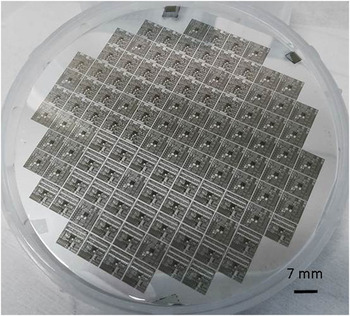
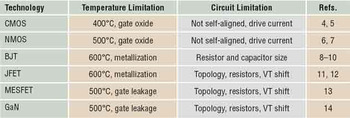
Since larger diameter (100–150 mm) SiC substrates with defect densities low enough for reasonable yields are now available, ICs using SiC can certainly be realizedReference Kimoto and Cooper3 (Figure 1). Using SiC, operation of both junction field-effect transistors (JFETs) and bipolar circuits have been demonstrated up to 600°C, and metal oxide semiconductor field-effect transistor (MOSFET) circuits have been able to operate up to 500°C (Table I). Circuit complexities are currently far behind silicon complementary metal oxide semiconductors (CMOS); silicon has had more than 40 years to reach maturity. Even so, SiC circuits with several hundred devices, both digital and analog, have been fabricated. The performance of SiC circuits at room temperature is far worse than silicon counterparts, but reliability is anticipated to improve in the 200°C to 300°C range as compared to silicon.Reference Cressler and Mantooth1 The temperature regime of interest is >300°C, where silicon technology cannot operate at all, for instance space missions to the inner planets.Reference Cressler and Mantooth1 What is also clear is that the present demonstrations of 600°C operation is not limited by SiC itself, as devices using SiC could possibly work up to 1000°C.Reference Zetterling2 Other materials involved, mainly for metallization and passivation, are now the limiting factors in terms of operational temperature.Reference Kimoto and Cooper3 Packaging is a separate issue with huge challenges ahead, and reliability testing is only in its infancy with just a few tests conducted for 1000 hours.
Processed 100-mm-diameter wafer with bipolar SiC integrated circuits.Reference Lanni16 The chips are 7 × 7 mm2 in size.

Performance limitations and state-of-the-art SiC integrated circuit technologies.

Note: CMOS, complementary metal oxide semiconductor; NMOS, n-type metal oxide semiconductor; BJT, bipolar junction transistor; JFET, junction field-effect transistor; MESFET, metal semiconductor field-effect transistor; VT, threshold voltage.
This article reviews different SiC technologies based on MOSFET, JFET, metal semiconductor field-effect transistor (MESFET), and bipolar transistors. The capabilities demonstrated so far, as well as the main features and limitations, are outlined. At present, it is unclear which circuit technology will prevail, but what is certain is that SiC ICs will soon become commercially available for high-temperature applications.
Applications
There are two obvious application areas for high-temperature ICs: sensing and power circuits/energy conversion.Reference Cressler and Mantooth1 For sensing, there are many gas and pressure sensors available that can work as high as 600°C.Reference Kimoto and Cooper3 If the signal is too weak and there is no possibility of cooling the electronic parts, a SiC amplifier could be considered. Sensor interfaces could also include analog-to-digital conversion, memory for storage, and data transmission.Reference Cressler and Mantooth1
Higher temperatures are often encountered for power circuits and energy conversion. Even if SiC power devices are commercially available, driver circuits and failure monitoring are necessary and currently limited to Si devices and Si operating temperatures. If a separate cooling system for the electronics can be avoided, large savings can be realized due to reduced cost and weight and improved reliability using SiC circuits. As of right now, SiC devices have found applications in aerospace, oil and gas drilling, and monitoring of high-temperature combustion or incineration processes. If the required operation temperature is above 300°C, silicon will simply not be an option, so the higher price of SiC substrates and ICs is not necessarily an issue. Another area for SiC ICs is applications where the temperature is on the borderline for silicon, around 200°C. As a rule of thumb, failure rates double for every 10 degrees of temperature increase.Reference Cressler and Mantooth1 A technology such as SiC ICs capable of operation at 600°C is expected to be more reliable than silicon ICs, which fail around 250°C. However, this must be demonstrated with ICs made in a close-to-commercial process.
Properties of SiC
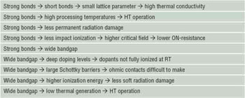
SiC is a material with only covalent silicon–carbon bonds, which are much stronger than silicon–silicon bonds but weaker than carbon–carbon bonds. Almost all of the properties of SiC can be explained by these stronger bonds, as shown in Table II. Stronger bonds lead to shorter bonds, a smaller lattice parameter, and higher thermal conductivity. Higher processing temperatures are needed to break these bonds, but it also implies that ICs can operate at high temperatures. External ionizing radiation can break bonds, but strong bonds imply that immunity to permanent radiation damage should be higher. In reverse biasing conditions, less impact ionization occurs, leading to possible higher critical fields and, in turn, to lower ON-resistance under forward bias (see Equations 1–3 below for details) when thinner and higher doped blocking regions are fabricated. The wide bandgap is also a result of the atomic structure. With wide bandgaps (Table II), deeper ionization levels for dopants and thereby incomplete ionization of dopants at room temperature can unfortunately be expected. In addition, Schottky barriers between metal and semiconductor tend to be larger, making ohmic contacts on SiC more challenging. However, higher ionization energies reduce the sensitivity to ionizing radiation and associated single event upsets. Finally, the thermal generation of carriers is much lower, allowing higher operating temperatures. Overall, although high-voltage devices and high-temperature ICs look promising for commercialization, there is a tradeoff between challenging manufacturing and improving electrical performance.
Connections between properties of SiC.

Note: HT, high temperature; RT, room temperature.
The almost 10 times higher critical field for breakdown compared to silicon is the reason for the great interest in SiC as a material for high-voltage devices.Reference Zetterling2 In the OFF-state, a reverse-biased low-doped junction blocks the current, but in the ON-state, the resistance of this low-doped region will dominate the ON-resistance. A higher critical field E C translates to a proportionally thinner blocking region W (Equation 1) with higher doping concentration N D (Equation 2). The specific ON-resistance R ON actually scales inversely with the critical field to the cubic power (Equation 3).Reference Zetterling2 Here, q is the elementary charge, ε is the relative dielectric constant, and μn is the electron mobility.
 $${V_{\rm{B}}} = {{{E_{\rm{C}}}W} \over 2}\,and\,thus\,W = 2{V_{\rm{B}}}/{E_{\rm{C}}}$$
 $$W = \sqrt {{{2{\rm{\varepsilon }}{V_{\rm{B}}}} \over {q{N_{\rm{D}}}}}} \leftrightarrow {N_{\rm{D}}} = {{2{\rm{\varepsilon }}{V_{\rm{B}}}} \over {q{W^2}}} = {{{\rm{\varepsilon }}E_{\rm{C}}^2} \over {2q{V_{\rm{B}}}}}$$
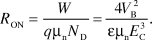 $${R_{{\rm{ON}}}} = {W \over {q{\mu _{\rm{n}}}{N_{\rm{D}}}}} = {{4V_{\rm{B}}^2} \over {\varepsilon {\mu _{\rm{n}}}E_{\rm{C}}^3}}.$$
However, the ON-resistance also scales as the square of the breakdown voltage V B. For voltages below 100 V, the ON-resistance no longer dominates, and it is mostly at voltages above 1000 V that the advantages of SiC become obvious. This means that for ICs, the critical field is unimportant at the present level of integration.
The thermal conductivity is also less important as long as self-heating is not limiting performance. The intention with high-temperature ICs is to operate at a high ambient temperature, so there is no large temperature gradient for removing the heat. At low temperatures, not all dopants are ionized in a semiconductor. For silicon, full ionization occurs at room temperature but not at, for example, 77 K.Reference Kimoto and Cooper3 SiC on the other hand does not reach full ionization until 200°C or 300°C.Reference Kimoto and Cooper3 This is not a problem for high-temperature ICs operating above 200°C, but can be something to keep in mind for applications where the ICs will work in a wide temperature range. Starting from room temperature, resistances decrease because of the incomplete dopant ionization; however, above 200°C or 300°C, the increased scattering dominates, so all resistances increase as expected.Reference Kimoto and Cooper3 For modeling of resistances versus temperature, this has to be carefully taken into account.
The wide bandgap also affects the built-in voltage (the voltage needed to significantly forward bias p-n junctions). In silicon, this is typically 0.7 V; whereas in SiC, it is approximately 2.5 V. Circuit designers use this for the voltage drop across a diode or the base-emitter junction. In power transistors, this causes extra power loss in the driver circuitry, and for ICs, higher supply voltages generally need to be used, perhaps 15 V rather than 5 V. The built-in voltage is reduced by 2 mV/°C, both for silicon and SiC. For SiC ICs that work in a wider temperature range, this must be carefully considered. On the other hand, there are temperature compensation circuits exploiting exactly this phenomenon, using bipolar junction transistors for reference voltage generation in precision analog-to-digital converters and other circuits.Reference Cressler and Mantooth1
The main reason for the failure of silicon at temperatures above 300°C is the intrinsic carrier generation. The concentration of thermally generated electron-hole pairs n i is exponentially dependent on the bandgap E g and the temperature T, according to Equation 4 (where N C and N V are the effective number of states in the conduction and valence bands, respectively, and k is Boltzmann’s constant).
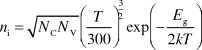 $${n_{\rm{i}}} = \sqrt {{N_{\rm{C}}}{N_{\rm{V}}}} {\left( {{T \over {300}}} \right)^{{3 \over 2}}}{\rm{exp}}\left( { - {{{E_{\rm{g}}}} \over {2kT}}} \right)$$
When thermally generated carriers start to reach the levels of the carriers in the semiconductor, this first results in excess noise. Germanium transistors (bandgap of 0.66 eV) were notorious for this behavior; even at 70°C, reception quality suffered in transistor radios using GE transistors. As the concentration of thermally generated carriers further increases, excess junction leakage will heat the semiconductor so bit-errors occur or a runaway condition starts. This is critical in silicon microprocessors. The intrinsic temperature refers to the temperature where the semiconductor can no longer be used, and this depends on the background doping. For bulk silicon, this is around 250°C, whereas SOI can generally be used to 300°C, since devices are dielectrically isolated. The corresponding temperature for SiC is theoretically as high as 1000°C, and devices and circuits have been tested up to 600°C without any sign of this being the limitation.Reference Kimoto and Cooper3
Reliability at 600°C is a different question. Accelerated lifetime testing with commercial devices is usually done by either increasing the applied electric fields or heating to around 300°C to achieve earlier failures.Reference Cressler and Mantooth1 SiC ICs are expected to work at much higher temperatures and at somewhat higher fields than where silicon ICs are reliability tested. New testing methods will have to be developed for testing reliability of operation at temperatures above 300°C. This will happen in time, as SiC ICs are going to find widespread use in high-temperature application areas. For operation at 250°C, SiC ICs that work at 600°C are bound to have an edge over silicon SOI that fails above 300°C.
Processing of SiC MOSFETs
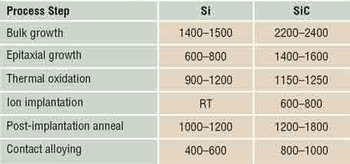
Wafer sizes and material quality for SiC have improved over time. At present, both 150 mm and 100 mm wafers are available with low enough defect densities for reasonable device yields. Epitaxial layers with n- or p-type doping can be grown close to specifications with low variation in thickness and doping concentration across the wafer. For research purposes, the total processing yield is definitely high enough. There is no commercial fabrication of SiC ICs at this point, although some vendors offer multi-project wafer service for university research using either n-type metal oxide semiconductor (NMOS) or CMOS. The main difference between the processing of silicon and SiC wafers for ICs is the temperature range involved,Reference Kimoto and Cooper3 as is listed in Table III. The strong bonds between silicon and carbon atoms require more energy for growth of the material, post-annealing of damaged material after ion implantation, and bond breaking during thermal oxidation or contact alloying. The only advantage is that diffusion of dopants is practically non-existent, such that doping profiles will stay sharp even with large temperature budgets.Reference Zetterling2
Process temperature ranges for Si and SiC in °C.*

Note: RT, room temperature.
*For details, see Reference 3.
Bulk and epitaxial growth of SiC will not be covered here, as it is covered elsewhere in this issue and in the literature.Reference Kimoto and Cooper3 Growth is also performed first in the process and hence its temperature budget is not as big of an issue for IC processing. Thermal oxidation is the only process step where temperatures are in about the same range as the growth of SiC, but it instead has many challenges with interface charges and reduced effective channel mobility. Some aspects of gate oxide reliability will be mentioned later.
It is difficult to remove damage after ion implantation in SiC. Elevated temperatures are often used during ion implantation, so hard masks composed of silicon dioxide or metal, rather than photoresist, have to be used. During the high-temperature anneal after ion implantation, the surface must be protected from silicon depletion. This can be done by covering the wafer with a carbon cap made from photoresist; annealing it inside a SiC container; or by supplying a silicon overpressure in the annealing furnace.Reference Kimoto and Cooper3 Even so, there is noticeable damage remaining after ion implantation. As a result, ion implantation-free processing has been investigated for bipolar ICs in SiC.Reference Lanni, Malm, Östling and Zetterling9 Finally, metal contacts are alloyed at a higher temperature in SiC compared to silicon. Unfortunately, the higher temperatures involved in ion implant annealing and contact alloying have made self-alignment techniques used for silicon MOSFETs inaccessible for SiC MOSFETs, thereby limiting the gate length scaling to ∼1 µm.
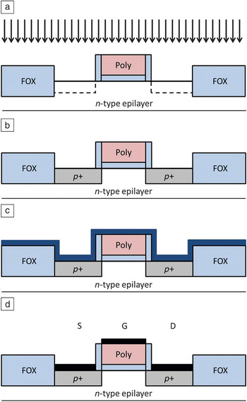
To understand this last statement, we consider Figure 2. A simplified typical silicon MOSFET process (here illustrated for p-channel devices) starts with field oxide formation, gate oxidation, gate polysilicon deposition and etching, and gate spacer formation. The source and drain implants can now be performed self-aligned to the polysilicon gate and the field oxide, Figure 2a. Photoresist is only used to mask n-channel devices. No matter how short the gates have been etched in the previous step, the implant is exactly aligned to the gate spacers. After ion implantation annealing, the p+ source and drain are slightly diffused, but this process is well controlled, Figure 2b. The key to this process step is that both the gate oxide and the polysilicon gate can withstand the ion implantation anneal at 1200°C. The second self-aligned step is the formation of silicided source, gate, and drain by the salicide (self-aligned silicide) process. Next, metal is deposited but not patterned, Figure 2c. In a two-step anneal, a silicide is formed between the metal and exposed silicon, but the temperature is low enough that reaction does not take place between the metal and silicon dioxide in the spacers and field oxide. Finally, the excess metal is wet etched selectively to the metal silicide before the final anneal step finishes contact alloying, Figure 2d. Typical metals used are nickel, titanium, and cobalt. Note that for very short gate lengths, self-alignment offers the best precision possible.
Simplified self-aligned silicon metal oxide semiconductor field-effect transistor process flow. (a) Ion implantation of p-type dopants (arrows) into source and drain (dashed boxes) is self-aligned to the field oxide and polysilicon gate with oxide spacers (i.e., no extra mask is needed). (b) After ion implantation annealing, the source and drain dopants are activated and diffuse slightly. (c) Metal is deposited over the transistors (dark blue) and annealed without masking. Silicides will form only on top of the silicon, but not on SiO2 (field oxide [FOX] and gate spacers). (d) After wet-etching of the unreacted metal, the silicide (black) remains on all contact areas. Note: poly, polycrystalline silicon gate; S, source; D, drain; G, gate.

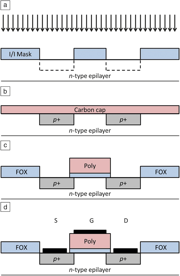
In comparison, the SiC MOSFET process in Figure 3 cannot take advantage of this self-alignment. There are no gate dielectrics or gate materials available that can withstand ion implant annealing temperatures for p-type dopants of 1600–1800°C, and even gate replacement schemes would require some material to survive on the surface. Because the ion implantation itself is usually done at elevated temperatures, a hard mask has to be used (Figure 3a). A carbon cap is used to protect the surface during the annealing step to avoid silicon depletion from the surface (Figure 3b). Only after this high-temperature process is the field oxide, gate oxide, and gate polysilicon deposited and patterned (Figure 3c). Alignment needs to be done to global alignment marks initially etched in the SiC wafer before the implant mask is made. Considerable overlap is thus needed between gate, source, and drain, thereby limiting gate length scaling to maybe 1 µm at best. Not even the source and drain contacts can be self-aligned due to the higher temperatures involved (Figure 3d). At 800–900°C, the metal will react with both silicon and silicon dioxide at the same time, thus resulting in short circuits.
Simplified non-self-aligned SiC metal oxide semiconductor field-effect transistor process flow. (a) Ion implantation of p-type dopants (arrows) into source and drain (dashed boxes) is performed with an ion implant hard mask. (b) During ion implantation annealing, the surface has to be protected with a carbon cap, which prevents Si out-diffusion and surface roughening even at 1800°C. (c) The field oxide (FOX) and polycrystalline silicon gate (poly) stack is aligned with global alignment marks (not shown), and some overlap must be allowed. (d) The metal must be patterned before annealing at 800–900°C to form the metal silicide (otherwise the reaction will occur with the SiO2). Note: FOX, field oxide; I/I Mask, ion implant hard mask; S, source; D, drain; G, gate.

n-type ion implanted material can be annealed at 1200°C, allowing for self-aligned NMOS ICs. However, NMOS circuitry requires normally ON depletion load transistors, often made by an extra ion implantation step in the channel. For CMOS, several ion implants are used: n+ and p+ for source and drain in n- and p-channel transistors, respectively, and at least one implant for p-well or n-well formation.
The largest challenge for MOSFET-based ICs is the low inversion mobility in the channel.Reference Kimoto and Cooper3 For silicon MOSFETs, the rule of thumb is that an effective mobility of approximately 50% of the bulk mobility results in a well-designed gate oxide process if electric fields are limited. In SiC MOSFETs, this mobility is only 10%, and since hole mobility is already very low, the drive current suffers. For balanced silicon CMOS gates, the width of p- and n-channel devices have a ratio of 2:1 to compensate for the differing channel mobilities, but for SiC, a ratio of almost 5:1 would be necessary.Reference Young, Clark, Cormack, Murphy, Smith, Thompson, Ramsay and Finney5 This greatly affects integration, drive current, fan-out, and switching speeds of digital ICs.
The reason for the lower channel mobility in SiC MOSFETs is not entirely understood. It partially results from interface traps in the channel, so at higher temperatures, the channel mobility improves slightly. It is not possible to counteract this with increasing gate voltage overdrive, since the electric field in the gate dielectric, usually silicon dioxide, has to be limited to avoid dielectric breakdown. For power MOSFETs, there is a maximum voltage rating that strictly limits the current drive and ON-resistance. For ICs operating at high temperatures, the conditions will approach that of accelerated lifetime testing, and this is probably why SiC CMOS and NMOS ICs have only been demonstrated up to 400°C or 500°C, respectively (see Table I).
For power MOSFETs, the electric field in the OFF-state also needs to be considered. Close to the blocking junction, the electric field is close to the critical field of SiC, and the electric field in the oxide is higher by a factor of 2.5 (around 6 MV/cm) due to the ratio of dielectric constants in the two materials.Reference Kimoto and Cooper3 This is usually not an issue for SiC ICs, and in silicon MOSFETs, the corresponding field is only 0.3 MV/cm.Reference Kimoto and Cooper3
Finally, the temperature variation of the threshold voltage has to be considered. Since it is reduced by about 1 V for every 100°C change, threshold voltages have to be designed with some safety margin at the highest temperature expected. At room temperature, the threshold voltage will be high, and supply voltages need to be greater than 5 V.
Processing of SiC bipolar ICs
With all the challenges for MOSFET ICs, it is not surprising that other technologies have been investigated for SiC ICs. Inspired by III–V transistors, an epitaxial growth plus mesa etch design was investigated for power and IC bipolar transistors.Reference Lanni, Malm, Östling and Zetterling9 Since this device can be made entirely without ion implantation, several of the high-temperature processing steps can be removed. The remaining damage after ion implantation can also lower the current gain.
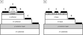
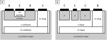
A cross-section of a SiC npn transistor is shown in Figure 4a, in comparison with the standard ion implanted silicon npn transistor in Figure 5a. The SiC IC process uses five epitaxial layers and three mesa etches to make fully junction-isolated transistors. Adding just one etch step makes lateral pnp transistors possible with the same epitaxial layersReference Lanni, Malm, Östling and Zetterling15 (Figure 4b). In comparison, the silicon npn is ion implanted with a resulting planar topology (Figure 5a) as well as the possibility of lateral pnp transistors (Figure 5b). Integrated resistors are easily implemented in both technologies in either the emitter or base layers.
Cross-sections of SiC mesa-etched (a) vertical npn and (b) lateral pnp transistors. These devices can be made entirely without ion implantation. All epitaxial layers with their respective doping concentrations are grown on the SiC wafer, and then several steps of dry etching are performed to create the required structures. Only one extra etching step is needed to make the lateral pnp transistors. Note: B, base; E, emitter; C, collector.

Cross-sections of silicon ion-implanted (a) vertical npn and (b) lateral pnp transistors. All doped regions are defined using different ion implantation steps, resulting in a planar surface. No extra step is needed for the lateral pnp transistors. Note: B, base; E, emitter; C, collector.

Bipolar transistor degradation has previously been reported for SiC, but is now mostly under control thanks to improved epitaxial growth.Reference Kimoto and Cooper3 Of course silicon dioxide is also used in the bipolar process for surface passivation and intermetallic isolation, but the electric fields across the oxide are much smaller than in a gate oxide and therefore not a limitation. The drawback with this SiC technology is the cost of epitaxial layers, and the resulting topology with several micrometer-sized steps.Reference Lanni, Malm, Östling and Zetterling9 Step coverage for the metallization is a challenge. Reliability at 600°C is mainly dependent on metal integrity rather than transistor operation.
The incomplete ionization has some effects on the current gain. As base dopants are ionized, the current gain is reduced from room temperature and up to 300°C, but then it improves slightly when the minority lifetime in the base improves at higher temperatures.Reference Lanni, Malm, Östling and Zetterling9 For integrated resistors, the resistance values first decrease when ionization increases with increasing temperature, but at higher temperatures, the mobility decreases as scattering increases. Both of these temperature effects have to be modeled when designing ICs. However, analog circuits normally use feedback with ratios of resistors with similar temperature coefficients (such that the absolute values are not important) to maintain stable performance over wide temperature ranges. Stable operation seldom relies on absolute values of current gain or resistance in the devices. The drift of the built-in voltage of the pn-junctions mentioned previously is consistent and predictable, in comparison to the threshold voltage drift in MOSFETs.
JFET, MESFET, and GaN ICs
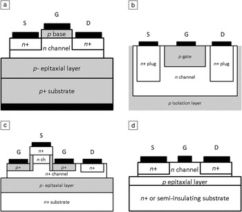
This overview is not complete without including JFET, MESFET, and GaN ICs, especially since the first ICs in SiC were made using JFETs. The motivation was that these could be made with only n-type ion implantation and had lower requirements on p-type contacts,Reference Neudeck, Garverick, Spry, Chen, Beheim, Krasowski and Mehregany11 see Figure 6a. The design requires p-type substrates, which are normally more expensive and have lower material quality. Operation up to 600°C has been demonstrated.Reference Neudeck, Garverick, Spry, Chen, Beheim, Krasowski and Mehregany11 The drawback with the lateral JFET is that it is normally ON and only has n-channel devices. For an IC technology, this requires level shifters and resistive pull-ups. Resistors are easily integrated by removing the gate region of a transistor.
Lateral junction field-effect transistor (JFET) in (a) SiC and (b) silicon, (c) vertical JFET in SiC, and (d) metal semiconductor field-effect transistor in SiC. The silicon JFET in (b) is made using only ion implantation, whereas all the SiC FETs in this figure use a combination of epitaxially grown doped layers that are patterned by dry etching and ion implantation requiring high-temperature annealing. Note: S, source; D, drain; G, gate; ch, channel.

In silicon technology, there are hardly any pure JFET ICs, even if JFETs can easily be integrated in a bipolar process using the same ion implants, see Figure 6b. At some point JFETs were used as high impedance input stages for bipolar operational amplifiers, and the TL081 series of silicon general purpose operational amplifiers are still available. The vertical JFET can be made on n-type substrates, and by varying the channel width by etching, both enhancement and depletion mode devices can be made simultaneously, Figure 6c. However, still only one channel polarity is available, and voltage level shifters are usually required in circuits.
The MESFET structure is similar to the JFET, except the gate is metal only; there is no p-region, Figure 6d. In this case, a Schottky junction controls the channel transport. At high temperatures, Schottky gates are notoriously leaky, and above 300°C, they will degrade. Otherwise, they have the same drawbacks as JFET ICs. Similar to this is GaN HFET IC technology, except here the gate is a heterojunction with better isolation properties.Reference Cressler and Mantooth1 At higher temperatures, degradation occurs. An important difference with JFETs is that semi-insulating SiC substrates can be used, which reduces parasitic drain capacitance and hence improves high-frequency performance. Both SiC MESFETs and GaN HFETs have excellent high-frequency performance with large power per gate width,Reference Cressler and Mantooth1,Reference Kimoto and Cooper3 and this is where these ICs will be used, but at room temperature; they are usually referred to as monolithic microwave integrated circuits (MMICs). All of these technologies suffer from the same threshold voltage drift as MOSFETs.
Summary
Some performance metrics and challenges are collected in Table I. Apart from the MMICs, the performance of SiC ICs is worse than silicon ICs at room temperature. The capability of operation above 300°C and expected higher reliability as compared to silicon’s capabilities above 200°C is the motivation for continued research on SiC ICs.
One could ask whether uncooled SiC devices could find application in high-performance computing where cooling requirements are becoming tougher as clock frequency and power consumption increases. However, the level of miniaturization for SiC ICs is far from that of silicon (by a factor of more than one million at present), and this is surely far into the future.
A common limitation for all SiC IC technologies, not related to the type of device, is the lack of high-temperature packaging and capacitors. Although ceramic packages can probably withstand higher temperatures than those cited in their current ratings, capacitors are a bigger challenge since high capacitance values require thin dielectrics that degrade at high temperatures and electric fields, similar to the gate oxides of MOSFETs. Although 5 V operation has been demonstrated for SiC CMOSs, higher supply voltages are generally required due to the larger built-in voltage of 2.5 V as compared to the 0.7 V for silicon. This offers higher noise margins and variations with temperature, but interconnecting with silicon ICs is a challenge.
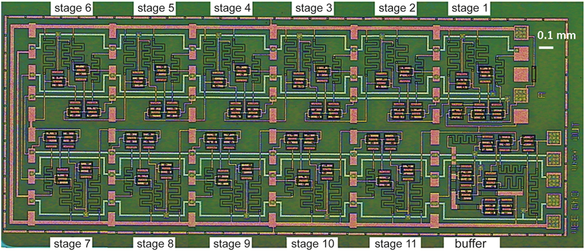
This article has demonstrated that SiC makes high-temperature electronics possible up to 600°C. An example of such a technology is illustrated with the close-up of an 11-stage ring-oscillator with two-layer metallizationReference Lanni, Malm, Östling and Zetterling15 in Figure 7. Presently, metallization and packaging are limiting operating temperatures. Although the technology choice is unclear, advances have been made in device types, and SiC devices should be commercially available in increasing quantities going forward.
Fabricated 11-stage SiC ring-oscillator with two metal layers with 53 transistors and 53 resistors.Reference Lanni16 The chip is 3.7 mm × 1.5 mm in size, and the square bonding pads are 0.1 mm × 0.1 mm.

Acknowledgments
All SiC colleagues and PhD students at KTH (present and former) are acknowledged for their contributions to the in-house bipolar SiC technology. The Swedish Foundation for Strategic Research is acknowledged for funding the HOTSiC project.