I. INTRODUCTION
TRENDS for future wireless communication indicate a multiplication of standards and a rationalization of RF front-end blocks to be more versatile. Such evolution requires technological abrupt changes (in particular for receivers) with ultra-compact solutions for antennas, impedance matching, and filters. This could be realized by introducing multifunctional materials such as magneto-dielectric (MD) heterostructures which may use simultaneously ferromagnetic (F), antiferromagnetic (AF), and ferroelectric (FE) properties [Reference Garello, Viala and Bènevent1]. Such materials are based on the ability to grow high-quality thin films with a variety of precisely controlled composition and interfaces. The multilayer deposition technique becomes a versatile toolbox to design new materials based on existing knowledge of single materials. This provides an outstanding opportunity to realize new RF materials with artificial physical responses. One exciting challenge here is to create a material combining a high permeability (μ) and a high permittivity (ε) with adjustable properties (μ/ε), and being self-biased up to ~20 GHz.
The aim of this work is to provide a proof of concept for this unusual class of materials to be suitable for size reduction of RF components such as half-wavelength (λ/2) resonators. The long-term objective is to design miniaturized antennas and filters based on such materials. In this paper, we use 2-cm-long coplanar waveguides (CPWs) to simulate λ/2 resonators having a resonance frequency close to ~3 GHz. Moreover, we develop an analytical model for multilayered CPWs to be loaded with such MD material. The results of the model are first compared to preliminary realizations using a single alternation heterostructure (150 nm thick) with μ = 150 and ε = 18. Then, the model is used to predict size reduction for λ/2 resonators when adjusting material properties (μ, ε).
This paper is organized as follows. First, the MD heterostructure properties are described. Then, experimental results for CPWs are shown. Finally, we present the analytical model and predictive results are discussed.
II. HETEROSTRUCTURE THIN FILM PROPERTIES
The MD heterostructure results of the assembly of high permeability thin films and high permittivity thin films with multiple alternations (n).
A) High permeability material
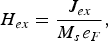
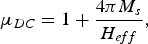
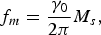
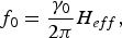
The high permeability material uses ultra-high magnetization F thin films. This material is combined with AF thin films. The AF/F interfacial exchange coupling is used to shift the F resonance (f FMR) of the F material at high frequency which also allows adjusting the DC-permeability (μDC) [Reference Lamy and Viala2]. In details, the exchange-coupled magnetic material consists of 25-nm-thick Fe65Co35 film (F) and 30-nm-thick Ni50Mn50 film (AF). Fe65Co35 alloy exhibits the highest known saturation magnetization (4πM s measured to 2.35 T) leading to ultra-high permeability when being polarized. The polarization is realized with using AF exchange bias with NiMn and adjusting the thickness of F (e F). Indeed, AF/F exchange coupling leads to a strong unidirectional anisotropy (H ex) for F which depends on e F−1 (see equation (1), where J ex is the interfacial energy). Finally, H ex contributes to the effective field (H eff) which drives both f FMR and μDC as shown in equations (2–3) where γ 0 is the gyromagnetic factor:

B) MD heterostructure
Usually, regarding the efficiency of wave-to-media coupling with magnetic thin films, thickness has to be significant (~1 µm). On the other hand, as ferromagnetic materials F (and Mn-based AF materials) are metallic, eddy currents become detrimental when increasing frequency. A well-known solution consists in laminating the magnetic materials with thin insulators such as standard low permittivity dielectrics (SiO2 or Al2O3).
Here, the challenge is to use perovskite materials as they exhibit very high permittivity values (ε ≥ 100). In particular, SrTiO3 (STO) is a promising candidate with an intermediate permittivity in the as-deposited state (ε = 18) and a high permittivity (ε = 150) in the crystallized state. Additionally, the crystallization temperature for STO can be lowered down to ~400°C which has been shown for CMOS (Complementary Metal Oxide Semiconductor) compatibility for MIM (Metal Insulator Metal) capacitors [Reference Guillian, Tartavel, Defay, Ulmer, Andre and Baume3]. This is a major advantage because it would make STO compatible with AF/F magnetic electrodes which are usually annealed at 300–400°C. This contrasts with the crystallization temperature of other perovskites exceeding ~600°C and being not compatible with any F (and AF) materials. In the middle term, the MD heterostructure combining high permeability and high permittivity would consist in an assembly of AF/F electrodes with STO, with multiple alternations ([STO/F/AF/F] × n).
In this work, the experimental results reduce to a preliminary stack consisting in: STO (50 nm)/FeCo (25 nm)/NiMn (30 nm)/FeCo (25 nm)/STO (50 nm) with μ = 150 and ε = 18. Results for other combinations (μ = 150–250 and ε = 18–150) will be predicted analytically.
III. EXPERIMENTAL RESULTS
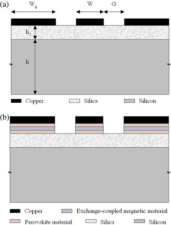
To provide a proof of concept for such MD materials to be suitable for size reduction of λ/2 resonators, we use 2-cm-long CPWs having a dimensional resonance frequency (f R) of ~3 GHz. The corresponding topology is shown in Fig. 1(a). It is a multilayered CPW structure including a high resistivity silicon substrate, a thick SiO2 insulator layer (thermal oxidation), and a metallization on top consisting in 500-nm-thick copper layer. As shown in Fig. 1(a), one defines W as the central conductor width, W g as the width of the lateral ground planes, and h 1 and h as the thicknesses of the silica layer and the silicon substrate, respectively. The structure of the loaded-CPW is shown in Fig. 1(b). The MD material is deposited on the top of the silica layer following by the metallization deposition. For easier fabrication (single lithography mask) both the MD film and the copper metallization are etched at the same time.
Structures of the unloaded-CPW (a) and loaded-CPW (b) on thermally oxidized silicon substrate.

The experimental results come from RF measurements which have been made with a two ports wafer probe station and using a 20 GHz Agilent N5230A vector network analyzer. A standard SOLT (short open load thru) calibration has been used.
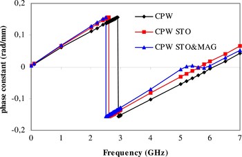
The significant parameter shown here is the phase constant (β) because it is proportional to the square root of the product of the effective permeability and the effective permittivity as indicated in
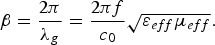
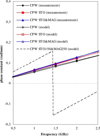
The frequency dependence of β is shown in Fig. 2. One considers three samples: unloaded-CPW (“CPW”) as the reference sample, loaded-CPW with STO only (“CPW STO”), and loaded-CPW with MD material (“CPW STO&MAG”). The two last cases allow separating dielectric to magnetic contributions. First, as expected, Fig. 2 indicates that β increases when loading with the MD material. This is consistent with the resonance frequency f R which shifts at lower frequencies (~15%). Second, when comparing with “CPW STO” at low frequency, the major contribution arises from STO. At higher frequency (i.e. close to f FMR where μ significantly increases with the F resonance), the magnetic contribution also clearly translates on β. In order to quantify the contributions of μ and ε to the size reduction of λ/2 resonators, one defines the potential of miniaturization (PM) from β as follows:

Phase constants of the unloaded- and loaded-CPWs (experimental results).

PM is calculated for a frequency band (Δf) from 10 MHz up to 2 GHz where Δβ and Δβref correspond to the change of β with and without the MD material. Indeed, PM has to be estimated below the f FMR where the magnetic losses are negligible and the slope of β is linear. From the experimental results, PM is of ~11% with STO only and of ~15% with MD. These results are noticeable with regard to the moderate thickness of the heterostructure used here (~150 nm).
IV. ANALYTICAL MODELING
A) Description of the model
An analytical model is now presented in order to predict size reduction for λ/2 resonators when adjusting material properties (μ, ε). In the last 10 years, remarkable progress with finite element simulation has led to a variety of numerical models for CPWs. But analytical models are still of interest because they are faster to use and helpful for first design. In this paper, the model predicts the frequency behavior of multilayered CPWs on a semiconductor substrate. The model is based on the original work of Heinrich [Reference Heinrich4]. First, the model is revised to take into account the high resistivity silicon substrate and the silica layer. Second, the model is completed to take into account the MD material with μ and ε as complex parameters.
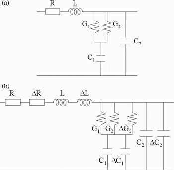
The analytical model uses a RLCG distributed elements description. The electrical equivalent circuits for the unloaded and loaded-CPW are shown in Fig. 3. The resistance R and the inductance L are calculated from [Reference Heinrich4] while new expressions are proposed here for the capacitances C 1, C 2 and the conductances G 1, G 2:




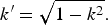
where ε req is the equivalent relative permittivity, σ s and tan δ e are the conductivity and the dielectric loss tangent of the silicon substrate, respectively. K is the complete elliptic integral of the first kind and the variables k and k′ are calculated as follows:

Electrical equivalent circuits for unloaded-CPW (a) and loaded-CPW (b) on thermally oxidized silicon substrate.

The analytical model for the MD loaded-CPW requires extra distributed elements to translate the effect of ε and μ. First, the equivalent relative permittivity is modified to predict the influence of the STO. Consequently, additional capacitances ΔC 1, ΔC 2, and conductance ΔG 2 are introduced (Fig. 3(b)) to reproduce the effect of ε and tan δ e of the STO, respectively. STO is considered as non-dispersive in the gigahertz range.
Second, real and imaginary parts of the permeability of the magnetic material are taken into account with introducing additional resistance ΔR and inductance ΔL in series with R and L of the equivalent circuit (Fig. 3(b)). As the permeability is highly dispersive in the gigahertz range, we introduce the frequency-dependence based on linearized Landau–Lifshitz–Gilbert equation [Reference Gilbert5, Reference Kittel6]. Because of the finite size of the magnetic material, the effects of the demagnetizing fields are taken into account [Reference Aharoni7]. One notes eddy current is neglected here as the thickness of the conductive magnetic layer is only of 50 nm which is much smaller than the skin depth (5 µm at 2 GHz):





where α is the damping constant of the magnetic material, V the magnetic volume, ω the angular frequency, and K c a calibration factor depending on the topology of the loaded- CPW. N x, N y, and N z are the demagnetizing factors, where x, y, and z are along the width, the height, and the length of the CPW, respectively.
B) Validation of the model
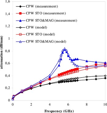
The frequency dependences of the attenuation constant α a and the phase constant β are shown in Figs 4 and 5. The figures cumulate experimental and theoretical results. As seen, for each configuration, the analytical model is consistent with the experimental behavior. Regarding α a, below the f FMR (≈5.5 GHz), the introduction of the MD material does not introduce significant degradations. Moreover, when comparing α a for the cases with STO only and with MD, one notes the excess losses mainly originate from STO. For the following, the discussion reduces to the 0.01–2 GHz frequency band where the degradation of α a with the MD material is negligible (≤15%).
Attenuation constant of the unloaded- and loaded-CPWs (analytical and experimental results).

Phase constant of the unloaded- and loaded-CPWs (analytical and experimental results).

C) Predictive results
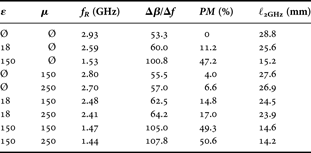
Now, the model is used to predict size reduction for λ/2 resonators when adjusting material properties (μ, ε). PM is evaluated for various values of (μ, ε). Also, one calculates the physical length (ℓ2 GHz) of a λ/2 resonator operating at 2 GHz for illustration. All the results are summarized in Table 1. First, we emphasize the dominant role of ε which contrasts to μ when respectively compared to the reference sample (lines 3 and 4 in Table 1). This would indicate the electric field concentrates more efficiently than the magnetic field in the MD material. Also, one notes the thickness of STO is twice larger than the thickness of F. Thus, when considering the cases where the permittivity has been increased up to ε = 150 (x ~ 8), which corresponds to the crystallized state of STO, PM is now of 47.2% (x ~ 4). Second, when increasing μ from 150 to 250 (×1.66), by reducing the f FMR at 4.2 GHz, one notes PM to increase (×1.75) in the same proportion as μ (lines 4 and 5 in Table 1). It would mean the device being more sensitive to a change in μ than in ε. Finally, by combining μ = 250 and ε = 150, one may predict a size reduction of ~50% while keeping the material thickness similar (~150 nm). The effect on the phase constant is illustrated in Fig. 5 (dashed line). To be substantial, one calculates the physical length of a λ/2 resonator (with f R = 2 GHz) which reduces here to 14.2 mm (in contrast to 28.8 mm).
Synthesis of the analytical results.
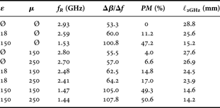
Analytical results concerning the potential miniaturization from various values of permittivity and permeability of the MD substrate.
In the future, larger size reduction can be expected with increasing the number of alternations of the material.
V. CONCLUSION
This paper is a proof of concept for the miniaturization of RF components such as λ/2 resonators with MD thin film heterostructures. It based on the idea of a material combining high permeability and high permittivity at microwave frequencies. A preliminary material with μ = 150 and ε = 18 is shown. It is used to partially load 2-cm-long CPWs. An increase of the phase constant and a shift of the resonance frequency of ~15% are measured. Then, a predictive model is proposed with μ and ε as variables. When adjusting the material properties in a realistic way (μ = 250 and ε = 150), the model predicts size reduction ≥50% for λ/2 resonators. This can be still improved with increasing the thickness of the material, that is by increasing the number of alternations (typically 2–5). Such material is also of interest for the miniaturization of antennas such as dipole and patch.
ACKNOWLEDGMENT
This work is supported by the French national agencies ANR – Instituts Carnot and DGA.
 Evangéline Bènevent (born in 1980) received the Ph.D. degree in electronics from the University of Jean Monnet, Saint-Etienne, France in 2006. She has worked successively at RADIALL and CEA-LETI in Grenoble (France) as a research engineer. Her research interests are magnetic and dielectric materials and associated devices for microwave applications.
 Kevin Garello received his Masters degree in fundamental physics at Brest University (France) in 2006. He is currently ending his Ph.D. degree at CEA-Grenoble on the subject of magneto-dielectric heterostructures thin films study and conception for microwaves applications.
 Dominique Cros received the Ph.D. degree in electrical engineering from the University of Limoges, Limoges, France in 1990.
In 1990, he became an Assistant Professor with the Faculty of Science, University of Limoges. From 1999, he is Professor with the Faculty of Science, University of Limoges. He currently conducts research with the Research Institute in Optical and Microwave Communications (IRCOM), which is became XLIM since 2006. His current research interests are planar and dielectric resonators for filters and oscillator applications at microwave frequency, electromagnetic tools to design microwave design and application of news materials in millimiter-wave systems.
 Bernard Viala Born in 1968, he received a Ph.D. degree in Physics at the National Institute of Applied Sciences of Toulouse (France) in 1994 on rapidly quenched magnetic materials. From 1994 to 1996, he joined the MINT Center of the University of Alabama (USA) as a post-doctorate research fellow studying soft nanocrystalline high magnetization thin films for magnetic recording. From 1996 to 2001, he worked successively at SILMAG and PHS-MEMS Saint-Egrêve (France) as a research engineer for advanced magnetic recording and RF Magnetic MEMS. In 2001, he joined the CEA-LETI in Grenoble (France) where he is in charge of magnetic materials and RF MEMS developments. His research interests include tunable RF devices, spintronics, and smart materials. He published over 40 papers and holds 20 patents.