I. INTRODUCTION
Dye-sensitized solar cell (DSSC) is a type of photoelectrochemical cell that provides more than 11% power conversion efficiency of solar energy. DSSC is composed of a dye-modified wide band gap semiconductor electrode, a counter electrode, and an electrolyte containing a redox couple (I−/I3−). Under sunlight illumination, the dye molecules adsorbed on the wide band gap semiconductor surface absorb light and become excited. Subsequently, an electron is injected from the excited state of the dye to the conduction band of semiconductor and then transfers to the transparent oxide. Finally, the electron flows through the external circuit.Reference O’Regan and Gratzel1–Reference Smestad, Bignozzi and Argazzi4 Recently, nanocomposite films have been of particular interest for DSSC device development owing to their controlled binary components and porosity. Preparation of a film on flexible organic substrates can make DSSC a commercially competitive technology as it allows the control of flexibility, weight, and overall device thickness. For example, DSSCs based on TiO2 films are regarded as low cost alternative cells for conventional semiconductor devices, which makes them of academic and practical interests.Reference Nazeeruddin, Kay, Rodicio, Humphry-Baker, Mueller, Liska, Vlachopoulos and Graetzel5–Reference Miyasaka9
Various methods have been proposed for preparing semiconductor films on a flexible substrate, such as sol–gel dip coating,Reference Yu, Zhao and Zhao10, Reference Zhao, Jiang, Zhang, Catterall and John11 spin coating,Reference Kasanen, Suvanto and Pakkanen12, Reference Watanabe, Nakajima, Wang, Minabe, Koizumi, Fujishima and Hashimoto13 sputtering,Reference Sirghi, Aoki and Hatanaka14, Reference Sirghi and Hatanaka15 spray pyrolysis,Reference Conde-Gallardo, Guerrero, Castillo, Soto, Fragoso and Cabañas-Moreno16, Reference Abou-Helal and Seeber17 atomic layer deposition,Reference Aarik, Aidla, Mändar and Uustare18, Reference Aarik, Aidla, Uustare, Ritala and Leskelä19 chemical vapor deposition,Reference Mills, Elliott, Parkin, O’Neill and Clark20, Reference Bessergenev, Pereira, Mateus, Khmelinskii, Vasconcelos, Nicula, Burkel, Botelho do Rego and Saprykin21 and electrodeposition.Reference Karuppuchamy, Jeong, Amalnerkar and Minoura22 Ink-jet printing technique is considered as a potential candidate that can provide mass production of low cost and uniform film deposition. This technique has been studied extensively as a research tool in materials and devices development due to the advantages of high reproducibility and easy production automation in comparison to dip coating techniques.Reference Kordás, Mustonen, Tóth, Jantunen, Lajunen, Soldano, Talapatra, Kar, Vajtai and Ajayan23–Reference Wu, Tamaki, Volotinen, Belova and Rao26
TiO2 is a well-known oxide because of its remarkable optical and electronic properties. Nanocrystalline TiO2 thin films are proved to have various applications in sensors, photocatalysis, and solar cells.Reference Rao, Kulkarni, Thomas and Edwards27, Reference Nanda, Narayan, Kuruvilla, Murthy and Sarma28 The problem of TiO2 is its inefficient charge transfer where the electron hops through the TiO2 thin films and exhibits a slow nonexponential current and charge recombination.Reference Gratzel29, Reference Nelson30 ZnO is another important semiconductor that has been widely investigated for its catalytic, electrical, optical, photochemical properties,Reference Kong, Sun, Li and Li31–Reference Hara, Horiguchi, Kinoshita, Sayama, Sugihara and Arakawa34 and for applications in blue/ultraviolet optoelectronic devices and in piezoelectric devices. It is known that semiconductors composites like (ZnO)1−x(SnO2)x,Reference Tennakone, Kottegoda, De Silva and Perera35 (CdS)1−x(MgO)x,Reference Bandaranayake, Jayaweera and Tennakone36 and (SnO2)1−x(MgO)xReference Tennakone, Bandara, Bandaranayake, Kumara and Konno37 show a lower power conversion efficiency than that observed for TiO2 film alone in a cell.
The combination of TiO2 with ZnO in a composite film is expected to reduce recombination rate by providing an energy barrier at the electrode/electrolyte interface leading to a reduced recombination of photoinduced electrons.Reference Kim, Yum and Sung38–Reference Zhang, Fu, Lv, Yang and Cao40 In this paper, we present a new approach, using ink-jet printing technique to produce the films. The DSSC is investigated by replacing TiO2 film with composite (ZnO)1−x(TiO2)x films with x = 0, 0.2, 0.5, 0.8, and 1 to elucidate the probable induced effect on the efficiency of the base DSSC.
II. EXPERIMENTAL
The semiconductor layers were printed by ink-jet technology from 1 M inks with multiprint passes. Five inks containing (i) 0.025 mol ZnO particles, (ii) 0.02 mol ZnO and 0.005 mol TiO2 particles, (iii) 0.0125 mol ZnO and 0.0125 mol TiO2 particles, (iv) 0.005 mol ZnO and 0.02 mol TiO2 particles, and (v) 0.025 mol TiO2 particles were added into 2-isopropoxyethanol (IPE) to form 25 mL suspensions for printing (ZnO)1−x(TiO2)x films where x = 0, 0.2, 0.5, 0.8, and 1, respectively. The five mixtures were ultrasonically agitated for 30 min in order to obtain suitable monodispersed suspensions for printing. The indium tin oxide glass substrates, used as the transparent conductive anode, were sonicated in acetone for 10 min followed by rinsing in isopropanol and dried by nitrogen gas to remove the acetone and unwanted contaminations. The substrates were heated to 80 °C before and during printing. The inks were deposited on the substrates by a piezoelectric shear mode drop-on-demand ink-jet printer using Xaar XJ126/50 printhead (XaarJet AB, Järfälla, Sweden). The as-deposited layers were dried in tens of seconds because of the substrate temperature (80 °C). To obtain films with suitable thickness for DSSC fabrications, the inks were printed layer by layer. We fabricated (ZnO)1−x(TiO2)x composite films consisting of 20 and 30 layers, respectively. The as-deposited films were then sintered in air at 600 °C for 1 h to completely evaporate the IPE solvent and condense the films.
The overall thickness of the (ZnO)1−x(TiO2)x film was determined by a dual beam focused ion beam/scanning electron microscope (FIB/SEM; FEI Nova 600 Nanolab, FEI Europe NanoPort, Eindhoven, Netherlands). X-ray diffractometer (XRD; Siemens D5000, Siemens AG, Karlsruhe, Germany) was used to detect the constituents of the semiconductor layer using Cu Kα irradiation (λ = 0.154 nm). The diffraction data were collected over a range of 20° ≤ 2θ ≤ 70° with a scan speed of 0.01°/step and 2 s/step.
The printed (ZnO)1−x(TiO2)x films were activated at 550 °C and left to cool down to 80 °C and immersed overnight in 3 × 10⁻⁴ M N3 dye solution (purchased from Solaronix Solaronix SA, Aubonne, Switzerland) in pure isopropanol. They were washed thoroughly by deionized water and then absolute ethanol and left to dry. The photoelectrode was sandwiched with Pt counter electrode prepared by magnetron sputtering and filled with liquid electrolyte consisting of concentration 0.5 M KI and 0.05 M I2 in ethylene glycol, over an area of 1.26 cm2. The fabricated cells were connected to variable resistors by aluminum wires, and the current/voltage of the cell was monitored by a multimeter.
III. RESULTS AND DISCUSSION
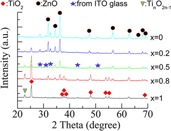
Figure 1 shows the XRD intensity patterns of the 30-layer printed (ZnO)1−x(TiO2)x composite films with different molar ratio of ZnO to TiO2. The scans were taken under the same condition, and therefore, the intensity of the peaks should be related to the quantity of the constituents. It is clear from Fig. 1 that as the ZnO molar concentration is increased, the relative intensity of diffraction peaks from ZnO [Joint Committee on Powder Diffraction Standards (JCPDS) No. 01-079–2205] is enhanced, while the relative intensity of diffraction peaks from TiO2 (anatase, JCPDS No. 00-002–0387) is reduced. The observed other titanium oxide phases (e.g., TinO2n−1) in the films, we believe, come from the chemical source of TiO2 particles.
XRD intensity patterns of (ZnO)1−x(TiO2)x composite films with varied x values.

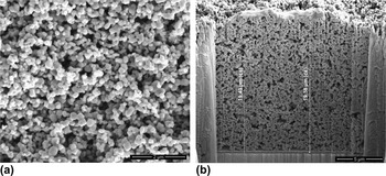
Figure 2 shows the typical SEM images and the FIB cross-sectional image of the 20-layer ink-jet-printed TiO2 film. From the images, the size of TiO2 particle was detected to be in a range of 70–400 nm with an average value of ∼170 nm. It is clearly seen from the cross-sectional image [Fig. 2(b)] that the film is uniform with thickness of ∼19.4 μm. The porous structure is observed in both the surface morphology and the cross-sectional images of the prepared films, which displays the large surface area for dye adsorption.
SEM morphology (a) and the FIB cross-sectional image (b) of TiO2 film.

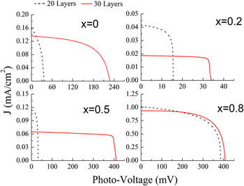
The effect of (ZnO)1−x(TiO2)x films thickness on the properties of solar cell has been investigated. Figure 3 shows the photocurrent density versus photovoltage (J-V) curves of solar cells prepared from 20- and 30-layered films for different constituent concentrations. For certain concentration solar cells, the short circuit photocurrent density (J SC) of the 20-layer samples is larger than that observed value for the 30-layer samples, while their open circuit voltage (V OC) is smaller. The film thickness dependence of J SC is related to: (i) the number of dye molecules adsorbed in the semiconductor films. The buildup of dye molecules in thicker film can generate more photoelectrons and thus result in higher J SC. (ii) The charge recombination between the ejected electrons and the I3− ions in the electrolyte. In thicker films, more photoelectrons are recombined with the electrolyte during the transport to the transparent conductive anode, which can decrease the J SC.Reference Wang, Kawauchi, Kashima and Arakawa41 We observed an increase of V OC with the thickness for all the films, especially for ZnO-dominate (ZnO)1−x(TiO2)x films (x ≤ 0.5). In thicker films, electrons transport along a longer path to complete the circuit. This increases the resistance of the cell, the charge recombination rate,Reference Wang, Kawauchi, Kashima and Arakawa41 and the possibility of back electron transfer.Reference Kang, Ryu, Chang, Park, Hong and Kim42 In addition, the photon localizationReference Zhang, Dandeneau, Zhou and Cao43 inside a thick film is more serious than in a thin film. These result in the V OC decrease with the thickness. On the other hand, it is known that in thick films, the capture of photons is better than in thin films. With the buildup dye molecules, the photovoltaic effect can be enhanced.
J-V characteristics of fabricated solar cells using 20- (dash lines) and 30-layer (solid lines) (ZnO)1−x(TiO2)x films, printed with different components concentration.

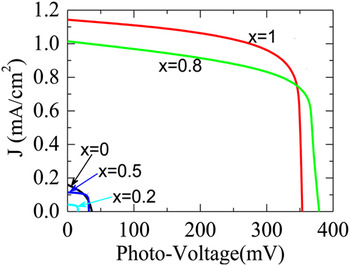
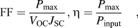
It is clearly seen from the curves that the J-V properties of solar cell depend on the molar ratio of ZnO to TiO2 in the films. In Fig. 4, we compare the photocurrent density–voltage (J-V) curves of solar cells fabricated from 20-layer (ZnO)1−x(TiO2)x films with different molar ratio of the components. It shows that the photovoltaic response of ZnO-dominated cells is much less than that of TiO2-dominated cells. The fill factor (FF) and the power conversion efficiency (η) were calculated according to:
 $${\rm{FF}} = {{P_{\max } } \over {V_{{\rm{OC}}} J_{{\rm{SC}}} }},{\rm{\eta }} = {{P_{\max } } \over {P_{{\rm{input}}} }}\quad,$$
Comparison of J-V curves of the solar cells fabricated from 20-layer (ZnO)1−x(TiO2)x films.

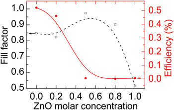
where P max is defined as maximum power, P input is the intensity of sunlight during the measurements (650–750 W/m2). Figure 5 shows the FF and the energy conversion efficiency of the cells with different ZnO molar concentration in 20-layer (ZnO)1−x(TiO2)x composite films. It demonstrates that ZnO decreases the energy conversion efficiency, from 0.52% for pure TiO2-based solar cell to 0.46% for the cell with (ZnO)0.2(TiO2)0.8 and finally less than 0.01% for ZnO-dominated solar cells. The dramatic influences of the component of the semiconductor layer on the performance of DSSCs could be attributed to the following: (i) the instability of ZnO in dye solution. It is reported that the acidic dye could dissolve Zn atoms and form Zn2+/dye complex resulting in insufficient dye adsorption and photoelectron generation and thus resulting in a poor performance of DSSCs.Reference Zhang, Dandeneau, Zhou and Cao43 (ii) Unlike the chemisorption in TiO2, pure ZnO layers do not easily absorb enough amount of the ruthenium complex dye. (iii) Even though the TiO2 and ZnO have similar band gap energy, their conduction band structures are different: Ti4+ has empty 3d orbitals (1s 2 2s 22p 6 3s 23p 6), while Zn2+ has empty 4s orbitals (1s 2 2s 22p 6 3s 23p 6 3d 10). Therefore, their density states and the electronic coupling strength with dye adsorbate are different. This results in the differences in electron injection rate from dye to their conduction band. For instance, the ejection time scale of photoelectron into ZnO conduction band is 1.5–150 ps (10−12 s), while for TiO2, it takes <100 fs (10−15 s).Reference Anderson, Ai and Lian44 The faster electron injected into the conduction band of TiO2 can reduce the recombination of electrons with the I3− ions in the electrolyte, and hence, the electron injection efficiency is higher and cell performance is better. (iv) The advantage of using ZnO in DSSC is the higher electron mobility than in TiO2 (2 order of magnitude higher), which may improve the performance of the cell by minimizing the charge recombination during the transport of the photoelectrons.Reference Tiwana, Docampo, Johnston, Snaith and Herz45
Plot of FF (dash line) and energy conversion efficiency (solid line) versus the molar concentration of ZnO (the value of 1−x) in (ZnO)1−x(TiO2)x films.

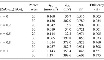
Notice that the 30-layer (ZnO)0.2(TiO2)0.8 film-based cell has a higher power conversion efficiency than that of pure TiO2-based cell (Table I). This might be caused by proximity effect of ZnO among TiO2 particles and retard charge.
Photovoltaic properties of ink-jet-printed solar cells based on (ZnO)1−x(TiO2)x films.

IV. CONCLUSIONS
(ZnO)1−x(TiO2)x composite films with nanosized porous structure have been prepared from ZnO and TiO2 nanoparticles via ink-jet printing. By changing the molar ratio of ZnO to TiO2 in the ink, the constituent concentration of (ZnO)1−x(TiO2)x films has been successfully modified. Based on these films, solar cells have been fabricated and the cell performances have been measured. The results indicate that the solar cell fabricated with thinner (ZnO)1−x(TiO2)x films have higher short circuit current density but lower open circuit voltage than thicker films. On increasing the ZnO concentration in (ZnO)1−x(TiO2)x films, the power conversion efficiency of the cell is found to decrease. Possible reasons for such a decrease are discussed.
ACKNOWLEDGMENTS
We thank Dr. Lyubov Belova for carrying out the SEM images and determination of the thickness of the (ZnO)1−x(TiO2)x composite films using the FIB system. We also thank Yan Wu and Wolfgang Voit for many discussions they did on the ink-jet printing process. Mei Fang acknowledges China Scholarship Council for her Ph.D. study fellowship. This research program has been conducted under the auspices of a MEENA research links grant by the Swedish International Development Agency (SIDA) Dnr. 348-2007-6992.