I. INTRODUCTION
Unconventional crystallographic orientations of perovskite substrates have garnered much attention recently for their potentially new functional interfaces.Reference Chakhalian, Millis and Rondinelli1 An exciting topological insulator originating from complex orbital order in transition metal perovskite oxide (111) heterostructures has been theoretically confirmed.Reference Rüegg and Fiete2 It has also been found that [110]-oriented manganite epitaxial films are more promising to make magnetic tunnel junctions because of their resistance against electronic phase separation,Reference Bachelet, Pesquera, Herranz, Sánchez and Fontcuberta3–Reference Tebano, Orsini, Castro, Medaglia and Balestrino5 which makes us more desirous to discover more intriguing effects as well as their corresponding crucial challenges.Reference Chakhalian, Millis and Rondinelli1 At present, perovskite oxide films grown on [001]-oriented substrates are controllable and becoming increasingly routine.Reference Chakhalian, Millis and Rondinelli1, Reference Zhang, Meng, Wang, Wang, Guo, Zhu, Yang and Zhang6 However, for the potentially functional [110]- and [111]-oriented films, corresponding growth exploration is greatly lacking. Many challenges and/or unknown factors could affect the film growth, or some novel properties could be obtained for unanticipated device applications.Reference Chakhalian, Millis and Rondinelli1 For example, the polar state of different substrate surfaces may be different, and thus, the perovskite oxide film systems could be driven to form different types of functional interfaces.Reference Chakhalian, Millis and Rondinelli1, Reference Reyren, Thiel, Caviglia, Kourkoutis, Hammerl, Richter, Schneider, Kopp, Rüetschi, Jaccard, Gabay, Muller, Triscone and Mannhart7 Meanwhile, the sharpness of the interface could be destroyed by these surface polar discontinuities.Reference Nakagawa, Hwang and Muller8 Moreover, the surface energy of (110) and (111) perovskite oxides is always higher than (001) perovskite oxides,Reference Yu, Heifets, Kotomin and Maier9, Reference Heifets, Goddard, Kotomin, Eglitis and Borstel10 and their surface reconstructions are fairly complex,Reference Enterkin, Subramanian, Russell, Castell, Poeppelmeier and Marks11, Reference Russell and Castell12 which means that the growth mechanisms of perovskite films on (110) and (111) substrates could be relatively complicated.
For colossal magnetoresistant Nd1−xSrxMnO3/SrTiO3 films, the corresponding phase composition and physical properties are unusual when grown on SrTiO3(110). Bulk-like behaviors were only observed in Nd0.5Sr0.5MnO3/STO(110) films.Reference Lai, Nakamura, Kundhikanjana, Kawasaki, Tokura, Kelly and Shen13, Reference Nakamura, Ogimoto, Tamaru, Izumi and Miyano14 Amazingly, unique filamentary metallic domains of Nd0.5Sr0.5MnO3 on SrTiO3(110) were found aligning preferentially along certain crystal axes of SrTiO3(110).Reference Lai, Nakamura, Kundhikanjana, Kawasaki, Tokura, Kelly and Shen13 A crucial factor for these phenomena is believed to be the anisotropic strain effect of SrTiO3(110). Moreover, a new type of orbital ordering exhibiting a clear first-order transition was also observed in this film.Reference Wakabayashi, Bizen, Nakao, Murakami, Nakamura, Ogimoto, Miyano and Sawa15 In addition, it is reported that the in-plane magnetism of another manganite La2/3Ca1/3MnO3 film can be tuned by the anisotropy of the SrTiO3(110) substrate.Reference Infante, Ossó, Sánchez and Fontcuberta16 These results suggest that the anisotropic SrTiO3(110) substrate is a new choice to modulate the properties of manganite films, which may enable us to fine tune the Jahn–Teller distortion for manipulation of the metal–insulator transition.Reference Ogimoto, Nakamura, Takubo, Tamaru, Izumi and Miyano17 Nevertheless, the detailed microstructure behaviors of Nd1−xSrxMnO3/SrTiO3(110) systems remain unclear, as well as the possible defects.
To understand the interplay of structure, magnetism, and electronic transport properties, the microstructural information of these film devices is inevitably required. (Scanning) transmission electron microscopy [(S)TEM], being able to provide a direct local interpretation of chemical, structural, and even electronic information of the interface at the atomic scale, is a very powerful tool to investigate film structures, especially in studying the defects and interfaces in thin films.Reference Wang, Zhu, He, Lu and Ma18–Reference Zhu, Zheng, Ma, Feigl, Alexe, Hesse and Vrejoiu20 In this paper, we report on a detailed study of microstructures and defects of Nd0.45Sr0.55MnO3 (NSMO) thin films grown on SrTiO3(110). The film was identified with a two-layer structure consisting of an epitaxial layer grown on the substrate and a nanostructured layer following the epitaxial layer. High-density planar defects were observed in the nanostructured layer with an in-plane translational displacement of 1/2a<111>. These findings may provide some information on growth mechanisms and on correlations with the unique properties of NSMO/SrTiO3(110) films.Reference Zhang, Meng, Wang, Wang, Guo, Zhu, Yang and Zhang6
II. EXPERIMENTAL
NSMO films were grown on STO(110) substrate by pulsed laser deposition method (550 mJ, 2 Hz). A KrF excimer laser beam was used with the wave length of 248 nm. Before deposition, the substrate was heated at 750 °C for 20 min to clean the substrate surface, and the laser was focused on the ceramic NSMO target to clean the target surface. During the whole deposition process, an oxygen pressure of 40 Pa and the substrate temperature of 750 °C were maintained. The film was then annealed at 750 °C in an oxygen pressure of 2 × 10⁴Pa for 10 min and cooled to room temperature with a cooling rate of 5 °C/min. Detailed experimental procedures can be found elsewhere.Reference Tang, Zhu, Meng, Zhang and Ma21
Transmission electron microscopy (TEM) specimens for cross-sectional observations were prepared by slicing, gluing, grinding, dimpling, and finally ion milling. Specimens for plan-view observations were ion milled only from the STO side.
A Tecnai G2F30 TEM (FEI Company, Hillsboro, OR) equipped with a high-angle annular dark field (HAADF) detector, which was operated at 300 kV, was used for electron diffraction analysis, high-resolution transmission electron microscopy (HRTEM) imaging, and high-resolution scanning transmission electron microscopy (HRSTEM) imaging. The point resolutions of the TEM are 0.20 and 0.17 nm for the TEM and STEM modes, respectively.
III. RESULTS
A. General information
NSMO is known as an A-type antiferromagnetic manganite. The uniformly aligned d x 2−y 2-type orbital has been recognized as being able to control the transport properties in its metallic phase.Reference Meng, Zhang, Wang, Tang, Wang, Zhu, Zheng and Zhang22–Reference Yoshizawa, Kawano, Fernandez-Baca, Kuwahara and Tokura24 At room temperature, the bulk NSMO has a body-centered tetragonal structure, which belongs to the I4/mcm space group with a lattice parameter a = b = 0.5390 nm and c = 0.7778 nm.Reference Kajimoto, Yoshizawa, Kawano, Kuwahara, Tokura, Ohoyama and Ohashi25 In this paper, the NSMO crystal will be treated as a slightly distorted pseudocubic structure for simplicity. The average (pseudocubic) lattice parameter should be a = 0.3837 nm.
B. The microstructure and interface of NSMO/STO(110) thin films
Figure 1(a) shows a cross-sectional low-magnification STEM image of NSMO/STO(110). The thickness of the film is about 200 nm. The interface is fairly flat and sharp. It is noted that the film exhibits a two-layered structure: a continuous layer with 30 nm thickness, which is directly grown on the substrate, and a nanostructured layer, which is grown from the continuous layer. The nanostructured layer is columnar like with an average width of 40 nm for each column. Figure 1(b) is a selected area electron diffraction (SAED) pattern taken from the area covering both the NSMO film and STO substrate. 330 diffraction spots for both the pseudocubic NSMO and STO are arrowed as seen in inset. The subscripts “S” and “F” denote “substrate” and “film,” respectively. A vertical arrow marks the body-centered tetragonal diffraction spots of NSMO. Besides the strong diffraction spots from both the film and the substrate, no extra spots were observed in the diffraction pattern, indicating that the NSMO film is well crystallized and has definite epitaxial relationships with the substrate, even for the nanostructured layer.
(a) Cross-sectional low-magnification HAADF-STEM image of NSMO/STO(110) heteroepitaxy showing the morphology of the films. The film exhibits a two-layer structure: an epitaxial layer directly grown on the substrate and a nanostructured layer following the epitaxial layer. (b) Composite diffraction patterns of both the film and the STO substrate indexed as [1 $\bar 1$0] zone axis of STO.

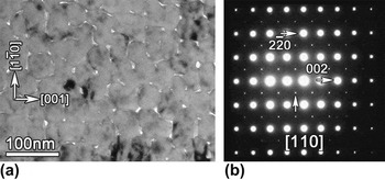
To observe the nanostructured layer in more detail, a plan-view sample was prepared. Figure 2(a) is a plan-view low-magnification TEM image of the NSMO film showing the columnar layer only, directly reconfirming the nanostructured appearance again. Figure 2(b) is the SAED pattern corresponding to Fig. 2(a). It is indexed as the [110] zone axis of pseudocubic NSMO. A vertical arrow indicates the body-centered tetragonal diffraction spots of NSMO. This SAED pattern verifies the fact that the nanostructured layer is well oriented as a [110] single crystal.
(a) Plan-view low-magnification TEM image of the NSMO film viewed near the [110] zone axis of STO. The nanostructured layer is clearly seen. (b) Corresponding SAED pattern showing the well-crystallized film.

To study the interface of the present film, HAADF-STEM experiments were performed because of their high space resolution and high chemical sensitivity. Figure 3(a) is an atomically resolved HAADF-STEM image viewed along [001] STO showing the interface between the NSMO film and the STO(110) substrate. The position of the interface is denoted by a pair of arrows. No misfit dislocations can be found along the interface, implying that the film is coherently grown on the substrate. The uniform contrast from both the film and the substrate reveals the composition homogeneity. The inset is a line profile across the interface along the atom column marked with a box. According to this line profile, one can see that the interface is fairly sharp; the roughness of the interface is confirmed to be less than 2 unit cells. Figures 3(b) and 3(c) are atomically resolved HAADF-STEM images of the NSMO/STO(110) interface viewed along the [1 $\bar 1$0] and [
 $\bar 1$1
 $\bar 1$] directions of STO, respectively. The coherent interface can be directly confirmed again by checking the contrast change across the interface.
Cross-sectional HAADF-STEM images of the NSMO/STO(110) system view along different axes of STO: (a) [001], (b) [1 $\bar 1$0], and (c) [
 $\bar 1$1
 $\bar 1$]. The interface is coherent. The inset of (a) is a line profile showing the sharpness across the interface.

C. The planar defects in NSMO/STO(110) thin films
Further study indicates that high-density planar defects exist in the nanostructured layer. Figure 4(a) shows a low-magnification dark field (DF) TEM image of the NSMO/STO(110) film viewed near the [1 $\bar 1$0] STO under a two-beam condition. High-density planar lattice defects are observed, stemming from the first epitaxial layer and about 30–40 nm away from the interface. Some defects penetrate through the whole NSMO film, while others end in the film. Both these extend along the [110] growth direction as indicated. Figure 4(b) is the corresponding SAED pattern taken from the defect area. The spikes along the [001] direction signify a high density of (001) planar defects,Reference Zheng and Ma26 as indicated by arrows in this figure. To identify the character of this kind of planar defects, HRTEM and HRSTEM imaging analyses were performed. Figure 4(c) is a HRTEM image along [1
 $\bar 1$0] STO showing some parallel planar defects. It can be seen that these defects have a 1/2a<100> translational displacement, compared with a perfect perovskite unit cell. From previous studies of perovskite-based epitaxial films by other authors,Reference Suzuki, Nishi and Fujimoto27, Reference Mi, Jia, Faley, Poppe and Urban28 this contrast of lattice defects can only be recognized as a kind of the Ruddlesden–Popper (RP) planar fault with a 1/2a<111> translational displacement.Reference Ruddlesden and Propper29 However, one cannot infer the true structural information from a common phase contrast image because the image contrast may change greatly with different focus value and the aberrations of magnetic lens.Reference Jia, Houben, Thust and Barthel30, Reference Lentzen, Jahnen, Jia, Thust, Tillmann and Urban31 To eliminate the confusion, HAADF-STEM imaging was carried out. Figure 4(d) shows an atomically resolved HAADF-STEM image of the planar defect along [1
 $\bar 1$0] STO. Because the HAADF-STEM image is an incoherent image, the interpretation of this kind of image is much easier due to the direct correspondence of bright dots to atomic columns, and the intensity of the dots is strongly dependent on atomic numbers.Reference Pennycook32, Reference McGibbon, Browning, Chisholm, McGibbon, Pennycook, Ravikumar and Dravid33 It can be seen from Fig. 4(d) that the planar defect was directly imaged. The Nd, Sr, and O atomic columns at the defect area are aligned face to face with no Mn and O atomic columns inside them, implying that the defects indeed have a 1/2a<100> translational displacement. The inset illustrates the atomic structure of the defect. Nevertheless, one cannot identify the true translational displacement of RP faults from Fig. 4(d) only because both 1/2a[
 $\bar 1$11] (in-plane displacement, which is now inclined to the electron beam) and 1/2a[11
 $\bar 1$] (out-of-plane displacement, which is now vertical to the electron beam) are possible. These two displacements for the observed RP faults are equivalent. Further observations are needed to identify the specific translational displacement.
(a) Cross-sectional DF TEM image of the NSMO/STO (110) system taken with g = (002) showing high-density planar defects in nanostructured layer. The dotted wavy line indicates the initiation of the defects. (b) Corresponding SAED pattern of the defects area showing the spikes caused by the planar defects. (c) HRTEM image of the planar defects along [1 $\bar 1$0] of STO. (d) Atomically resolved HAADF-STEM image along [1
 $\bar 1$0] of STO showing the atom configurations of the planar defect. Filtered HRTEM images showing (e) single fault accompanied by a partial dislocation and (f) double faults accompanied by APBs, respectively.

Figure 4(e) is a cross-sectional filtered HRTEM image showing just one RP fault initiating from the epitaxial layer. The fault is marked by a vertical arrow and illustrated by the inset. A Burgers circuit reveals a 1/2a[001] displacement (partial dislocation) for the fault, as indicated. This is different from other groups’ reports on the [001]-oriented films, which believed that the partial dislocations carry a displacement of 1/2a<111>.Reference Suzuki, Nishi and Fujimoto27, Reference Mi, Jia, Faley, Poppe and Urban28 So it can be inferred that the RP faults should have another displacement component parallel to the electron beam, 1/2a[ $\overline 1 $10]. Finally, the displacement of these defects can be expressed as follows:
 $$1/2a[001] + 1/2a[\bar 110] = 1/2a[\bar 111]\quad.$$
This conclusion will be verified later by a direct plan-view observation. Moreover, since the partial dislocation has an in-plane component 1/2a[001], it will somewhat relax the misfit between the substrate and the film. Interestingly, no closure failure is found when the Burgers circuit surrounds two adjacent faults as indicated in Fig. 4(f). Instead of partial dislocations, a short segment of (110) antiphase boundary (APB) is formed to accommodate the lattice arrangement, though the contrast is weak. Two insets illustrate the atomic configurations of the APBs. Similar results were reported previously.Reference Mi, Jia, Faley, Poppe and Urban28 From the observations above, it is possible to infer that when there are an odd number of vicinal defects available, then, one 1/2a[001] partial dislocation is enough to satisfy the NSMO lattice translational period, while many (110) APB segments will simultaneously form with even number of stacking faults to accommodate the translational periods. We obtained plenty of HRTEM images, and this inference was further confirmed.
To further study the configuration of the RP faults, a plan-view observation is required. Figure 5 is a plan-view low-magnification DF TEM image showing the nanostructured layer of NSMO. The high-density RP faults revealed by straight lines can be clearly seen, which extend along the [1 $\bar 1$0] direction. Moreover, these RP faults possess two types of terminations along [1
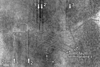
 $\bar 1$0], named I and II in Fig. 5, respectively. Type I means that the RP faults terminate in the grain matrix, while type II means that the RP faults terminate at pores. It should be specified that one straight line in Fig. 5 may comprise many RP faults, and they are not resolvable due to the resolution limit of the DF imaging technique. To study the details of RP faults with these terminations, HRTEM experiments were performed. Figure 6 is a plan-view HRTEM image showing the RP faults of type I. In Fig. 6, fault 1 and fault 2 extended along [1
 $\bar 1$0], while fault 1′, 2′, and 3′ extended along [
 $\bar 1$10]. These RP faults changed the translational period of the NSMO crystal, and thus, other defects may connect them to satisfy the perfect arrangement of NSMO, like (1
 $\bar 1$0) APBs. The dotted line in Fig. 6 denotes the (1
 $\bar 1$0) APB segments. If one counts the RP faults from the left to the right in Fig. 6, it will be found that the existence of the (1
 $\bar 1$0) APB segments depends on the number of the RP faults. In fact, this arrangement of the defects is the same as the cross-sectional ones in Fig. 4(f).
Plan-view low-magnification DF TEM image of the NSMO film taken with g = (002) showing high-density RP faults extended along [1 $\bar 1$0]. Two types of stacking faults were identified.

Plan-view HRTEM image along [110] STO showing the RP faults end in the grain matrix.

For RP faults of type II, the explanation is much more straightforward. As marked in Fig. 7, several RP faults were observed ending at a pore as denoted by vertical arrows. Although these RP faults are terminated by the pore, they may also change the translational period of NSMO around the pore. Indeed, partial dislocations or (1 $\bar 1$0) APBs have been observed. By drawing a Burgers circuit around the dislocation, the closure failure reveals that the Burgers vector of the partial dislocation is 1/2a[
 $\bar 1$11], which is the true displacement of the RP faults. This result confirms our previous inference that the RP faults possess an in-plane translational displacement. As to the (1
 $\bar 1$0) APBs, the dotted line denotes their positions.
Plan-view HRTEM image along [110] STO showing the RP faults end at pores. The whole translational displacement is determined as 1/2a[ $\bar 1$11].

IV. DISCUSSION
It is widely known that there are three major modes for thin film growth,Reference Martin, Chu and Ramesh34 namely:
(i) Island growth (Volmer–Weber mode),
(ii) Layer-by-layer growth (Frank–Van der Merwe mode), and
(iii) A combination of the above two modes (Stranski–Krastanov mode).
However, for perovskite oxides, compared with [001]-oriented films, the growth mechanisms for [110]-oriented films are still badly understood. If conditions are properly tuned, the [001]-oriented films could be grown layer-by-layer, thus high quality films could be produced.Reference Vrejoiu, Rhun, Pintilie, Hesse, Alexe and Gösele35 Moreover, the (001) surface of perovskite oxides are extensively investigated, and corresponding treatments were well developed to fabricate high quality films.Reference Kawasaki, Takahashi, Maeda, Tsuchiya, Shinohara, Ishiyama, Yonezawa, Yoshimoto and Koinuma36 But for the (110) surface, the structure and chemical information are still inadequately known. In addition, these (110) surfaces are anisotropic, polar, and severely reconstructed,Reference Enterkin, Subramanian, Russell, Castell, Poeppelmeier and Marks11, Reference Russell and Castell12 which may make the growth mechanisms more complicated. So it is relatively difficult to grow high quality [110]-oriented films with an atomically flat surface.Reference Bachelet, Pesquera, Herranz, Sánchez and Fontcuberta3 For the present NSMO/STO(110) films, the columnar structure of the upper layer indicates that the growth mechanism is island growth. Even for the lower epitaxial layer, the island growth mode still holds true in all probability because an uninterrupted layer-by-layer mode is unlikely to form the nanostructured layer. It is noted that the surface of STO(110) is fairly flat (Fig. 3). At the initiate stage of the film growth, this flat surface may allow the small islands of NSMO to coalesce perfectly with each other without the formation of defects like stacking faults and pores. So the epitaxial layer formed. In addition, as a commonly used substrate, the surface energies of different STO surfaces were studied and compared by some groups.Reference Yu, Heifets, Kotomin and Maier9, Reference Heifets, Goddard, Kotomin, Eglitis and Borstel10 The complex structures make the surface energies of STO(110) much higher, or at least, no less than STO(001). These results may suggest that the (110) surface of perovskite oxides is somewhat unstable, compared with the (001) surface. For the present NSMO system, as the film grows, the unstable NSMO (110) surface may become gradually coarsened causing incomplete island coalescence, and thus, the nanostructured columnar layer formed.
Moreover, as the NSMO film grows, some defects (like stacking faults) may form during the island coalescence (Fig. 4). We note that the surface reconstructions of perovskite (110) are very complex.Reference Enterkin, Subramanian, Russell, Castell, Poeppelmeier and Marks11, Reference Russell and Castell12 These reconstructions may result in the partial displacement of NSMO islands when they were deposited on the existing NSMO (110), and thus, the (110) APBs [Fig. 4(f)] and (1 $\bar 1$0) APBs (Figs. 6 and 7) formed. Furthermore, due to the limit of the lattice translational period, these APBs cannot end in the film without other accommodations. As a result, RP faults formed on the (001) side faces between two partially displaced islands. It should be noted that periodically arranged RP faults make a new crystal structure called RP phase,Reference Ruddlesden and Propper29 which implies that these defects in perovskite are relatively favorable for the energy consideration. So, compared with the {110} APBs, the RP faults in the present film are much more excessively distributed and most of them penetrate almost the whole upper column layer [Fig. 4(a)] and extend widely along the in-plane [1
 $\bar 1$0] direction (Fig. 5). In contrast, the {110} APBs just form short segments locally (Figs. 6 and 7). Furthermore, these RP faults play a key role to restrict the extent of the {110} APBs because most of the {110} APB segments ended with RP faults [Figs. 4(f) and 6].
It should be emphasized that for all three {100} faces of the present NSMO film, only the (001) face along the growth direction is RP faulted. This situation is different from the [001]-oriented filmsReference Suzuki, Nishi and Fujimoto27, Reference Mi, Jia, Faley, Poppe and Urban28 because the RP faults in these films occur more equally for the three {100} faces. We ascertain that for the [110]-oriented films, if the RP faults occur, they will tend to form (001) RP faults. According to the growth mechanisms discussed above, partially displaced NSMO islands will uniquely form (110) and (1 $\bar 1$0) APBs because of the special [110] growth direction. By checking the APB configurations, one will find that the (001) RP fault itself is enough to eliminate the {110} APBs. This is why only (001) RP faults were observed in the present film. Conversely, for the [001]-oriented films, considering the [001] growth direction, the (100) and (010) faces of the films are in an almost identical condition. Moreover, RP faults are nonconservative. Due to the composition undulation, the RP faults can directly form on the (001) face during the film growth. So all the three {100} faces of <001>-oriented films could be RP faulted.Reference Suzuki, Nishi and Fujimoto27, Reference Mi, Jia, Faley, Poppe and Urban28
Another feature of these RP faults in the NSMO/STO(110) is that they possess in-plane displacement only, namely, only 1/2a[ $\bar 1$1
 $\bar 1$] or 1/2a[
 $\bar 1$11] is possible, and they are equivalent. Theoretically, for a RP fault in cubic perovskite, four 1/2a<111> translational displacements are equivalent; only the partial dislocations connecting the RP faults will give the exact displacements. For the present film, both cross-sectional [Fig. 4(e)] and plan-view (Fig. 7) HRTEM images suggest that only the in-plane 1/2a[
 $\bar 1$11] displacement is reasonable. Again, this configuration is due to the specific growth direction of [110]. As discussed above, the NSMO islands will tend to form (110) and (1
 $\bar 1$0) APBs. Both these APBs have only in-plane 1/2a[
 $\bar 1$1
 $\bar 1$] or 1/2a[
 $\bar 1$11] displacement because only the highly reconstructed (110) faces and (1
 $\bar 1$0) faces of different NSMO islands can reasonably become faulted during the film growth. Naturally, the RP faults connecting the APBs will acquire an identical displacement.
V. CONCLUSION
The structures and the configurations of stacking faults in NSMO/STO(110) system were studied by (S)TEM. The NSMO film consists of an epitaxial layer directly grown on the substrate and a nanostructured layer following the continuous layer. High-density RP faults with an in-plane 1/2a<111> translational displacement were identified in the nanostructured layer, accompanied by 1/2a[001] partial dislocations or (110) APBs. Along the in-plane [1 $\bar 1$0] direction, the RP faults end at grain matrix or pores. Moreover, these energetically favorable RP faults play a key role to restrain the extent of {110} APBs in the NSMO film. The specific [110] growth direction is responsible for the special defect configurations and island growth mode in the present film. These findings may shed some light on understanding the film growth mechanism and potential defect formation of heteroepitaxial perovskite thin film systems grown on low symmetry substrate surfaces such as STO(110).
ACKNOWLEDGMENTS
This work was supported by the National Basic Research Program of China (Grant No. 2009CB623705) and the National Natural Science Foundation of China (Grant Nos. 51171190 and 51231007).