I. INTRODUCTION
In modern radio-frequency (RF) front ends, the required performances of power dividers (PDs) include spurious suppression [Reference Chau, Hsu and Tu1, Reference Mirzavand, Honari, Abdipour and Moradi2], differential ports [Reference Shi and Xu3], filtering integrations [Reference Li, Xue and Zhang4, Reference Chen, Huang, Shen and Wu5], high isolations [Reference Chao and Lin6, Reference Chao and Li7], high-power applications, compact size, low insertion loss, inherent DC-block function, and so on. Recently, there are several acceptable candidates for dual- or multi-function integrated PDs. For instance, by integrating a PD with two bandpass filters in [Reference Li, Xue and Zhang4], a three-port device can divide power and select frequency simultaneously. The co-design of PDs and filters [Reference Pal, Ghatak and Sarkar8–Reference Zhang, Xiao, Tang and Guo10] is a novel ideal for improving the integrity. Note that the isolation of the PD in [Reference Li, Xue and Zhang4] is not excellent. In addition, the filtering selectivity of filter-based PDs has been improved in [Reference Chen, Huang, Shen and Wu5] using complicated circuit structures. In order to enhance the isolation performance of filtering PDs, two different isolation structures have been proposed in [Reference Chao and Lin6, Reference Chao and Li7]. However, the filtering selectivity of the enhanced-isolation filtering PDs in [Reference Chao and Lin6, Reference Chao and Li7] is poor. Therefore, developing a simple-structure single-component PD with multi-function (larger than 3) integration becomes very urgent and difficult.
In this paper, a novel simple and compact filtering PD featured four-function integration is proposed. These four functions include high-selectivity filtering, inherent DC block between arbitrary two ports due to coupled-line sections, high all-frequency isolation, and high-power applications due to the grounded-connection resistor such as Gysel PDs. The clear design theory and approach of this novel PD is given. For experimental verification, a microstrip multi-function PD is designed, fabricated, and measured. The measured results show that high-selectivity and high all-frequency isolation performance is obvious.
II. DESIGN
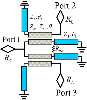
Figure 1 shows the circuit topology of the proposed multi-function filtering PD. The source and load terminated resistances are R S and R L , respectively. Two grounded transmission-line stubs with different characteristic impedances Z 2 and Z 3 are used to enhance the filtering selectivity and DC-shorted function (lightening protection design) for the three ports 1–3. A single resistor R Iso is employed not only to match ports 2 and 3 but also to provide high all-frequency isolation between two output ports 2 and 3, where the created heat can be properly dissipated through two grounded Z 3 stubs. Thus, this proposed filtering PD has high-power application feature of Gysel-type ones. The coupled-line section with even- (odd-) mode impedances Z e1 and Z o1 not only matches the two different terminated resistances, but also provides inherent DC-block function between two arbitrary ports.
Topology of the proposed multi-function filtering PD.

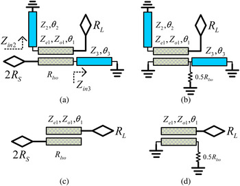
Based on the conventional even- and odd-mode excitations [Reference Chao and Lin6, Reference Chao and Li7], the even- and odd-mode equivalent circuits are shown in Figs 2(a) and 2(b). Due to the 0.5-π electrical lengths θ 2 = θ 3 = 0.5 π at the operating frequency, Figs 2(a) and 2(b) are simplified directly to Figs 2(c) and 2(d). Using the ABCD matrix in [Reference Zysman and Johnson11], the constraints for this PD are derived as
 $$2R_S = \displaystyle{\matrix{2(Z_{e1} + Z_{o1})R_L\sin \theta _1\cos \theta _1 + j[(Z_{e1}^2 + Z_{o1}^2 ) \hfill \cr \sin ^2\theta _1 - 2Z_{e1}Z_{o1}(1 + \cos ^2\theta _1)] \hfill} \over {2(Z_{e1} + Z_{o1})\sin \theta _1\cos \theta _1 + j4R_L{\sin} ^2\theta _1}},$$
 $$R_L = \displaystyle{\matrix{0.5R_{Iso}[(Z_{e1}^2 + Z_{o1}^2 )\sin ^2\theta _1 - 2Z_{e1}Z_{o1}(1 + \cos ^2\theta _1)] \hfill \cr - j2(Z_{e1} + Z_{o1})Z_{e1}Z_{o1}\sin \theta _1\cos \theta _1 \hfill} \over \matrix{(Z_{e1}^2 + Z_{o1}^2 )\sin ^2\theta _1 - 2Z_{e1}Z_{o1}(\cos ^2\theta _1 - 1) \hfill \cr - j(Z_{e1} + Z_{o1})R_{Iso}\sin \theta _1\cos \theta _1 \hfill}}. $$
Substituting θ 1 = 0.5π into (1) and (2), another simple version of constraints is established as
 $$\left\{ \matrix{Z_{e1} = Z_{o1} + 2\sqrt {2R_SR_L}, \hfill \cr R_{Iso} = 2R_L\left( {\displaystyle{{Z_{e1} + Z_{o1}} \over {Z_{e1} - Z_{o1}}}} \right)^{\!\!2}. \hfill} \right.$$
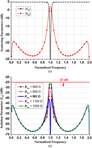
As a result, once the values of Z o1, R S , and R L are known, the accurate values of Z e1 and R Iso can be calculated using (3). A typical multi-function filtering PD example with numerical parameters R S = R L = 10, Z e1 = 113.3, Z o1 = 85, Z 2 = 70, Z 3 = 25, and R Iso = 983 Ω is simulated. The simulated results in normalized frequency band are plotted in Fig. 3.
Even- and odd-mode equivalent circuits and simplified ones of Fig. 1: (a) even, (b) odd, (c) simplified even, and (d) simplified odd.

The simulated results of the proposed multi-function filtering PD using ideal transmission-line models: (a) matching and transmission and (b) isolation.

The good filter selectivity and narrow bandwidth in the pass band is shown in Fig. 3(a). As illustrated in Fig. 3(b), the isolation of this PD example is still lower than −25 dB in all-frequency band (FBW = 200%) even though about ±20% variation of the single resistor is used. This indicates high adaptability in the choice of resistor values for achieving all-frequency excellent isolation of this proposed PD.
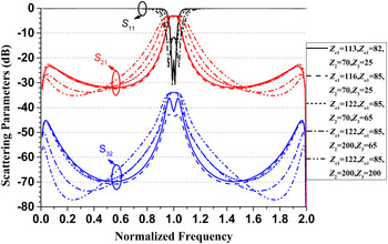
As for the filtering characteristic, it can be obtained by slightly tuning the parameters off the calculated values. The impedances of the stubs, including Z 2 and Z 3, do not affect the performance at center frequencies, but still have the impact on in-band bandwidths. Therefore, it is possible to control the bandwidths by choosing different sets of the parameter values and observing their simulated scattering parameters. One tuning example is shown in Fig. 4. In general, Z 2 = 70 and Z 3 = 25 Ω are chosen for achieving narrow-bandwidth filtering PDs.
Ideally simulated scattering parameters of the proposed PD with different sets of parameter values, where the isolation resistor is 983 Ω.

III. RESULTS AND DISCUSSIONS
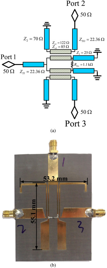
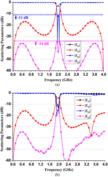
In order to further improve the band-pass selectivity of this filtering PD without affecting the isolation performance, the even-mode characteristic impedance Z e1 is optimized to 122 Ω, while a nominal value of the isolation resistor R Iso = 1100 Ω is applied in the final fabricated PD. As observed in Fig. 5(a), three extra 0.5-π transmission lines are applied to match the load impedances R S and R L to the standard 50 Ω ports. This circuit was fabricated on a F4B substrate with ε r = 2.65 and h = 1 mm when the operating frequency is 2 GHz. Figure 5(b) represents the corresponding photograph, and the dimensions of this prototype are marked in this figure. Since the three 0.5-π transmission lines (22.36 Ω) at outputs and at the input are introduced for measurements, the core part of the prototype merely includes the coupled lines and stubs, whose total dimension is 53.2 × 55.1 mm2. The simulated and measured results of this fabricated filtering PD are shown in Fig. 6. From the measured results in Fig. 6(b), it can be observed that the two measured reflection zeros of |S 11| about 2 GHz are 1.92 and 2.00 GHz (the theoretical values are 1.96 and 2.04 GHz), and the selectivity of this PD is greatly enhanced benefiting from these two reflection zeros. The measured −10-dB |S 11| bandwidth is about 6% (from 1.90 to 2.02 GHz). In addition, the measured isolation |S 23| is lower than −15 dB over the entire operation band (FBW = 200%).
The circuit configuration with accurate parameters (a) and photograph (b) of the fabricated multi-function filtering PD.

The simulated (a) and measured (b) results of the fabricated multi-function filtering PD.

To exhibit the advantages of this proposed PD, Table 1 is composed showing the comparison between the proposed PD and several state-of-the-art ones.
Performance comparison of the proposed device versus recent literatures.

IV. CONCLUSION
In this paper, a novel multi-function filtering PD is designed and fabricated. The advantages of high-selectivity filtering, inherent DC-block function, high all-frequency isolation, and high-power applications such as Gysel PDs have been achieved. Due to the simple circuit structure, convenient integration with other components, and easy design approach, this proposed multi-function filtering PD is an alternative for future advanced RF or millimeter-wave front ends.
ACKNOWLEDGEMENTS
This work was supported in part by the National Basic Research Program of China (973 Program) (Grant No. 2014CB339900), National Natural Science Foundations of China (Grant No. 61422103, 61327806, and 61671084), and BUPT Excellent Ph.D. Students Foundation (Grant No.CX2016202).
 Yongle Wu received the B.E. degree in Communication Engineering and the Ph.D. degree in Electronic Engineering from Beijing University of Posts and Telecommunications (BUPT), Beijing, China, in 2006 and 2011, respectively. From April to October in 2010, he was a Research Assistant at the City University of Hong Kong, Kowloon, Hong Kong. In 2011, he joined the BUPT and becomes currently an Associate Professor in the School of Electronic Engineering. His research interests include microwave components and wireless systems design.
 Lingxiao Jiao received the B.S. degree in Electronic Science and Technology from Beijing University of Posts and Telecommunications (BUPT), Beijing, China, in 2014. In September 2014, he started his research as a graduate at BUPT and is currently working toward the Ph.D. degree at the same university. His research interests include microwave passive components, power amplifiers, and RF systems.
 Jiayu Wang is an undergraduate student; he is currently in his final year of 4-year B.E. degree in Electronic Engineering at Beijing University of Posts and Telecommunications (BUPT), Beijing, China, in 2016. He will pursue his Master degree at the University of Science and Technology of China (USTC), Hefei, China, after his graduation. His research interests include microwave components and integrated circuits design.
 Weimin Wang received the B.S. degree in Communication Engineering, the M.S. in Electromagnetic Field and Microwave Technology, and the Ph.D. degree in Electronic Science and Technology from Beijing University of Posts and Telecommunications (BUPT), Beijing, China, in 1999, 2004, and 2014, respectively. In 2014, she joined BUPT. She is currently a Lecturer in the School of Electronic Engineering, BUPT. Her research interests include electromagnetic field and MIMO OTA measurement.
 Yuanan Liu received the B.E., M.E., and Ph.D. degrees in Electrical Engineering from the University of Electronic Science and Technology of China, Chengdu, China, in 1984, 1989, and 1992, respectively. From July, 1997, as a Professor, he is with Wireless Communication Center of College of Telecommunication Engineering, BUPT, Beijing, China, where he is involved in the development of the next-generation cellular system, wireless LAN, Bluetooth application for data transmission, EMC design strategies for high-speed digital system, and Electromagnetic interference (EMI) and Electromagnetic Susceptibility (EMS) measuring sites with low cost and high performance. He is interested in smart antennas for high-capacity mobile signal-processing techniques in fading environments, EMC for high-speed digital system, ISI suppression, orthogonal frequency division multiplexing (OFDM), and multicarrier system design. Dr. Liu is a Senior Member of the Electronic Institute of China.