I. INTRODUCTION
The search for appropriate ways to improve or change the functional properties of materials used in technological areas such as optics, electronics (including microelectronics), and magnetic devices creates a significant challenge. One of the possible approaches to this problem is modification by introducing distortions in the material. This results in a strained state that may lead to design of artificial materials with modified properties. Both crystalline and amorphous solids may exist in the strained state.
The crystalline strained state is characterized by elastic distortion of the lattice caused by internal stress. The inorganic fullerene-like nanoparticles and inorganic nanotubes can be attributed to the highly strained crystalline solids.Reference Tenne and Redlich1
Stress in a thin epitaxial film deposited on a substrate can appear due to a lattice mismatch and the thermal expansion mismatch between film and substrate. Thin films prepared by physical vapor deposition techniques exhibit high stress that is generated during the first stage of deposition by the particles adhering to the substrate.Reference Goudeau, Villain, Tamura, Celestre and Padmore2 Stress and stress relaxation play an important role in the initial stage of film growth, in film microstructure, and in degradation or enhancement of the properties of thin films (see, e.g., Refs. Reference Xie, Budnick, Hines, Wells and Woicik3 and Reference Choi, Biegalski, Li, Sharan, Schubert, Uecker, Reiche, Chen, Pan, Gopalan, Chen, Schlom and Eom4).
Properties of the strained epitaxial films markedly differ from the properties of the corresponding unstrained ones, and this difference is attributed to the structural distortions in strained film.Reference Choi, Biegalski, Li, Sharan, Schubert, Uecker, Reiche, Chen, Pan, Gopalan, Chen, Schlom and Eom4 A coherent distortion could arise at the interface between two or more thin layers in the multilayer structure.Reference Dagotto5 The contacted compounds must have chemical and thermal compatibility, and their structures must belong to a family with similar lattice constants allowing for a good match at the interfaces.Reference Dagotto5
In contrast to crystalline solids, the equilibrium amorphous state is stressed, and this stress is always a result of the specific preparation history of the material.Reference Alexander6 As shown in review,Reference Alexander6 amorphous films belong to one of three main classes of amorphous solids: random (but not periodic as in crystalline solid) “packing” of rigid particles in a stressed network. The packing has to be stable against structural buckling. The effect of initial stresses on the properties of an amorphous solid is crucial.Reference Alexander6 Stress in amorphous films can appear due to a thermal expansion mismatch between film and substrate.Reference Bowden, Brittain, Anthony, Evans, Hutchinson and Whitesides7 So, a thin film deposited on a thick thermally expanded polymer (the large volume expansion mismatch film/substrate) undergoes equibiaxial compression when the system is cooled. The stress relaxation is achieved by a buckling of the film into periodic structures.Reference Bowden, Brittain, Anthony, Evans, Hutchinson and Whitesides7 Stress-induced ordered shape structures arise in the amorphous magnetic filmReference Peng, Xie, Zhang and Zhong8 deposited on concave or convex surfaces of the mechanically bowed glass substrates. When a bowed substrate is removed from a holder, the substrate recovers its shape producing strains in the film.Reference Peng, Xie, Zhang and Zhong8
The first report on highly stressed amorphous filmsReference Lyahovitskaya, Zon, Feldman, Cohen, Tagantsev and Lubomirsky9 of BaTiO3 (BTO) (called quasiamorphous) possessing a piezo- and pyroelectric properties has been followed by experiments and theoretical research.Reference Frenkel, Ehre, Lyahovitskaya, Kanner and Lubomirsky10–Reference Feldman, Lyahovitskaya, Leitus, Lubomirsky, Wachtel, Bushuev, Vaughan, Barkay and Rosenberg14 The structure and chemical bonding in the quasiamorphous films were investigated using extended x-ray absorption fine structure (EXAFS)Reference Frenkel, Ehre, Lyahovitskaya, Kanner and Lubomirsky10 and x-ray photoelectron spectroscopy (XPS).Reference Ehre, Cohen, Lyahovitskaya and Lubomirsky11 As shown in Ref. Reference Frenkel, Ehre, Lyahovitskaya, Kanner and Lubomirsky10, the structure of the films is built from a random network of octahedral TiO6 local bonding units. These octahedra are connected to each other in three different ways: sharing apices, edges, or faces. Partial alignment of randomly connected distorted octahedra was considered to be the origin of polarity in the quasiamorphous phase.Reference Frenkel, Ehre, Lyahovitskaya, Kanner and Lubomirsky10 The oxygen XPS spectraReference Ehre, Cohen, Lyahovitskaya and Lubomirsky11 “of as-deposited” BTO and SrTiO3(STO) phases contain a strong satellite (shake-up) peak. This peak was interpreted as belonging to Ba and Sr- mediated oxygen-oxygen complexes. “The complex is not present in quasi- amorphous phase.” It was concluded that upon heat treatment the complex dissociated and presence of complexes in the “as-deposited” phase can be viewed as a “feature indicating possible formation of a quasiamorphous” phase.Reference Ehre, Cohen, Lyahovitskaya and Lubomirsky11
However, open questions still remain regarding stress control and the influence of the stress magnitude and mode of stress relief on the formation and stability of the highly stressed state. We propose that the major factor is the film/substrate adhesion energy (level of clamping).
II. EXPERIMENTAL
An experimental investigation was carried out using BTO, STO, and SrRuO3 (SRO) films that were attached to substrates (“clamped film”) and BTO and STO self-supported films (s-s film). Details of the film deposition procedure by RF sputtering on a substrate are described in Ref. Reference Lyahovitskaya, Zon, Feldman, Wachtel, Gartsman, Tagantsev and Lubomirsky12. A comprehensive study was carried out on the SRO thin films. The variable parameters included: the film thickness (100–800 nm), substrate material [Si (001), quarz, pyrex], presence or absence of a buffer layer (MgO or TiO2), and different substrate surface states (smooth or rough). The roughness was modified by grinding with multicrystalline diamond disks (1, 9, and 30 μm). Amorphous clamped films BTO and STO deposited on a treated Si surface were used to prepare the self-supported (s-s) films with lateral dimensions of 200–300 μm. The details of the s-s film preparation by local etching of the substrate are presented in Ref. Reference Lyahovitskaya and Lubomirsky13.
The postdeposition annealing of the films attached to the substrate and of self-supported films was carried out under isothermal conditions.
XRD was used to analyze the structure of the film. Structural homogeneity of BTO s-s films was investigated with x-rays at the ID11 beamline of the European Synchrotron Radiation Facilities (SR).Reference Feldman, Lyahovitskaya, Leitus, Lubomirsky, Wachtel, Bushuev, Vaughan, Barkay and Rosenberg14
XPS and EXAFS were used to characterize the structural and chemical changes in the films. EXAFS measurement was done at the beamline X18B of the National Synchrotron Light Source at Brookhaven National Laboratory, USA.
Surface morphology of the films was characterized by AFM, SEM, and by optical polarized microscopy. The internal structure of the s-s films was analyzed by optical polarized microscopy in transmitted and cross-polarized light.
III. RESULTS AND DICUSSION
A. Stresses in as-deposited amorphous film
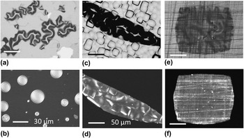
Figure 1(a) shows the adhesion failure of the amorphous SRO film deposited on a smooth surface of Si substrate. Stress relaxation occurs by buckling and by peeling. Stress decrease by the insertion of the amorphous buffer layer into the smooth surface leads to alteration of the buckling shape (circular blisters) shown in Fig. 1(b). However, in as-deposited films of SRO sputtered on a “treated surface,” no damage is observed. Above all, the as-deposited SRO films preserve their amorphous state irrespective of the substrate material, films stoichiometry, thickness (up to 800 nm), and the level or pattern of the roughness.
Optical images of surface morphology of as-deposited SRO (400-nm thick) films: (a) on smooth Si, (b) on smooth Si with amorphous buffer layer (TiO2, 50 nm). Top view in reflected light (c) and (e) and local areas without substrate in transmitted light (d) and (f) of two films: (c) and (d) on nonpolished side of Si and (e) and (f) on treated by 9-μm diamond.

AFM study (not shown here) and optical observation indicate that the treated substrate tracery is replicated in the film. Figures 1(c) and 1(d) show the images of surfaces and internal structures of two films sputtered on a treated substrates. One of them, BTO film, was deposited on the nonpolished surface of the one-side polished Si (c), and the other SRO was deposited on the treated substrate using a 9-μm diamond disk (d).
B. Stress evolution under postdeposited annealing
An amorphous film rigidly attached (clamped) to the substrate has difficulty in stress relaxation through shape change.Reference Alexander6 AFM measurements (not shown here) indicate that the surface of a SRO film after heating at various temperatures remains unchanged, relaxation by shape does not occur, and stress in the film grows with temperature.
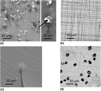
The amorphous state of SRO films with thickness up to ∼250 nm is preserved in the whole range of postannealing temperatures (300–500 °C). A noticeable difference is observed with changing deposition parameters that affect the magnitude of stress: an increase in the film’s thickness, change in clamped level, and film stoichiometry. Figure 2(a) shows damages on surfaces of as-deposited SRO film (400-nm thick) supported on a treated (1-μm diamond) substrate after annealing at 380 °C. No damage appeared in the SRO film that was supported on the substrate treated using 9-μm diamond after annealing at 450 °C [Fig. 2(b)]. Development of cracks in nonstoichiometric SRO films (400-nm thick) is evidence of increase in stress magnitude [Fig. 2(c)]. A noticeable difference is observed as the film’s thickness changed. Increase in the thickness can lead to a stress gradient across film, and in the areas, a long way from the film/substrate interface, the condition for crystallization may arise. As shown in Fig. 2(d), faceted crystals appear on the film’s surface of an annealed SRO film (thickness 800 nm).
Optical images of surface SRO films: (a) film (400-nm thick) on treated by 1-μm diamond after 380 °C, (b) film (400-nm thick) on treated by 9-μm diamond after 450 °C, (c) crack in nonstoichiometric (400-nm thick) film on treated by 9-μm diamond after 380 °C (SEM image), and (d) film (800-nm thick) on a treated by 9-μm diamond after 450 °C.

The question to be answered is what kind of processes in stressed amorphous films take part in the abatement of stress growing with temperature. Owing to the limited mobility in the film–substrate system, the stress enhancement with temperature can be relieved by transformation. Solid–solid transformation was thoroughly investigated experimentally and interpreted by thermodynamic analysis of the transforming “crystalline phases” (see, e.g., reviewReference Roytburd15). The mechanism of “amorphous–amorphous” transformation was not investigated. However, as was pointed out in Ref. Reference Roytburd15, many features of the transformation are typical for all phase transformations in solids. The solid–solid transformation is characterized by diffusionless strains and occurs by atomic rearrangement (displacement or shear processes of constituent units).Reference Roytburd15
Atomic rearrangement in SRO films (thickness 400 nm) sputtered “on a rough surface” was investigated using EXAFS. The changes in position of Sr and Ru atoms in all “annealed samples” relative to the “as-deposited ones” that similar to Ref. Reference Frenkel, Ehre, Lyahovitskaya, Kanner and Lubomirsky10 were revealed. An XPS study of BTO and STO films sputtered under conditions of “controlled stress magnitude and annealed at different temperatures” revealed that “the oxygen–oxygen complex is present in all annealed films as well.” The data (not included) show that the existence and disappearance of the oxygen–oxygen complex are correlated with the stress magnitude, and the complex dissociation is conditioned by high stress.
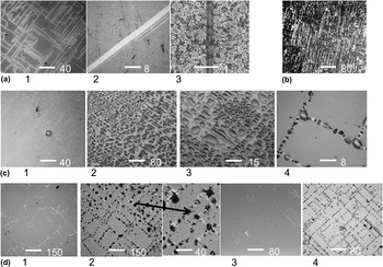
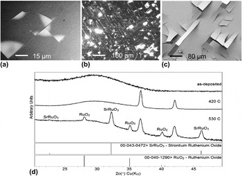
If the stress magnitude is high, the rearrangement of constituent units of the network (nondiffusive transformation) can diminish the stress. In the first stage of annealing, the stress increase leads to a change in the position of Ba or Sr relative to the oxygen octahedrons and to the formation of additional oxygen–oxygen complexes. Subsequent increases in stress can provoke the dissociation of the complex. The Ba or Sr coordination can be close to the position which these atoms occupy in perovskite structures and, in turn, can entail the displacement of Ti or Ru atoms inside an octahedron. The stress relief is achieved via stress redistribution, and the action of biaxial stress results in the formation of “the strain oriented structure of elastic domains.” The strain in the arranged structure is concentrated on the domain boundaries, which can be observed with an optical microscope [Figs. 3(a) and 3(b)]. The domain walls with smaller stress that are hidden on the film’s surface can be displayed using the condensation of chilled water vapor [Fig. 3(c)] or crystallization [Fig. 3(d)]. The boundaries with high stress can be a source of crack initiation [Figs. 4(a) and 4(b)] or can provoke delamination of the film from the substrate [Fig. 4(c)].
Amorphous polydomain structures: (a) optical and SEM images of boundaries: 1,2-STO, 3-SRO. (b) SRO (treated by 9-μm diamond, very density pattern), (c) BTO visualization by condensation chilled waters vapor: 1-initial surface, 2–4 with water (at different magnification), (d) visualization by crystallization: initial surface of STO (1) and SRO (3); surfaces with crystals (2,4).

Cracks on domain boundaries (a) BTO and (b) SRO; (c) delamination of nonstoichiometric SRO film (SEM images); (d) XRD patterns of SRO (400-nm thick) films: as-deposited, after 420 and 530 °C.

If the stress magnitude is too high and exceeds the elastic limit of the material, the stress may be relaxed via development of cracks or rupture the film. Such relaxation may occur as well in as-deposited [Figs. 1(a) and 1(b)] and in annealed films [Figs. 2(b) and 2(d)].
If the stress magnitude is low but the postannealed temperature is high, the viscous flows can arise. Incipient viscous flows provide mass transfer that promotes the coalescence (nucleus formation) that leads to crystallization. Atoms coordination in the nucleus can be close to the position in a perovskite structure or can be different from it. We detected an unknown crystalline structure in the SRO film annealed at 420 °C [Fig. 4(d)]. In the film annealed at 530 °C, crystalline phases of SRO perovskite structure and RuO2 arise [Fig. 4(d)].
C. Stress relaxation by shape change
Elastic energy stored in as-deposited clamped amorphous film is reduced by shape modifying during preparation of the self-supported (s-s) films by local substrate removal. Steadiness of “as-prepared s-s film” depends mainly on the thickness of the film and the initial stress in as-deposited film. As a rule, the higher the stress and/or the thinner the film, the probability of stress relaxation by fracturing is the greater. Alternatively, the relaxation of smaller stresses occurs by shape modification (e.g., buckling) and causes the s-s amorphous film to divide into regions with different curvature and density. Stress in the buckled film is distributed nonhomogeneously so that in regions adherent to the substrate, the stress may be high, while top regions are less stressed.Reference Goudeau, Villain, Tamura and Padmore16
Evolution of stress magnitude and density in BTO s-s films with thermal annealing was investigated. Our findings are as follows:
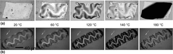
(i) Shape modification of as-prepared amorphous s-s films heated under an optical microscope in the range 20–180 °C is presented in Fig. 5. The initial planar shape of the film [Fig. 5(a)] becomes unstable at a certain critical stress level and the film is ruptured. Stress relaxation in the films with lower stress (buckled film) occurs both by shape modification and by densification (strain transformation) [Fig. 5(b)].
FIG. 5.Top view of the shape modification in as-deposited s-s BTO films by gradual increase temperature from RT up to 180 °C: (a) planar and (b) buckled.

(ii) Mass density evolution of as-prepared amorphous BTO s-s films with or without a polycrystalline buffer layer upon successive heating at a range of 300–600 °C is presented in Ref. Reference Ebralidze, Lyahovitskaya, Zon, Wachtel and Lubomirsky17. The experimental data unambiguously show that the film preserves its amorphous nature up to the crystallization temperature of amorphous BTO. The film undergoes “prenucleation expansion” and the density drops (∼400 °C). After that, the irreversible transformation is accompanied by densification and by film flattening.

Stress relaxation modes are specific for “each local area of the film” differing in thickness, curvature, stress magnification, and can occur via one of the following processes: shape modification, amorphous transformation, crystallization, and failure. The amorphous transformation results in strained elastic domains, and among them, highly strained arranged domains may be present. Such arranged domains acquire the anomalous birefringence that can be seen in cross-polarized light.
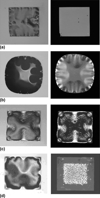
The diversity of structures of s-s BTO films annealed at ∼570 °C can be sorted roughly into three groups presented in Fig. 6: amorphous (with homogeneous stress and with stress anisotropy) [Fig. 6(a) and 6(b)], partially crystalline [Fig. 6(c)], and fully crystalline (excluding regions tethered to edges) [Fig. 6(d)].
Optical images in reflected and transmitted cross-polarized light of s-s BTO films after 570 °C: (a) and (b) amorphous, (c) partially crystalline and (d) fully crystalline (excluding amorphous areas tethered to edges).

It is important to note that though the stress evolution with temperature in local areas of the film occurs in a way that is analogous to that of a clamped film, the conditions favorable for nucleation and crystallization arise more frequently.
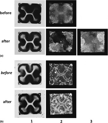
As follows from the general mechanism of crystallization of the amorphous phase (see, e.g., Ref. Reference Sokol, Kosevich and Givargizov18), the crystal growth related to discrepancies between the specific volumes of arising (crystalline) and initial (amorphous) phases and to internal stress level. As the specific volume of crystalline phase is usually less than that of the amorphous phase, internal stresses occur, which are proportional to the specific volume discrepancy.Reference Sokol, Kosevich and Givargizov18 Nucleation and growth are determined by internal stress levels and by modes of discrepancy compensation.Reference Sokol, Kosevich and Givargizov18 Discrepancy compensation in an amorphous film can occur through elastic strain or by shrinkage. Interstress relaxation can occur by viscous flow in the amorphous phase or by failure. As shown in Ref. Reference Feldman, Lyahovitskaya, Leitus, Lubomirsky, Wachtel, Bushuev, Vaughan, Barkay and Rosenberg14, the action of the x-ray SR led to the “local stress relaxation in a fully amorphous film” BTO annealed at ∼570 °C and initiated the growth of single crystal pyramids. Figure 7 shows the result of SR action “on the partially crystalline films.” A marked difference can be perceived in the BTO films before and after SR action. In the almost fully crystalline film [Fig. 7(a)], the SR action initiates the oriented crystallization and the recrystallization. It is manifested in the appearance of a large domain with closely orientated crystallites. The stress relaxation by SR action can lead to shape modification and to the film flattening [Fig. 7(b)].
Optical images in reflected (1), transmitted cross-polarized (2), and transmitted (3) light of two (annealed at 570 °C) s-s BTO films before and after x-ray synchrotron irradiation.

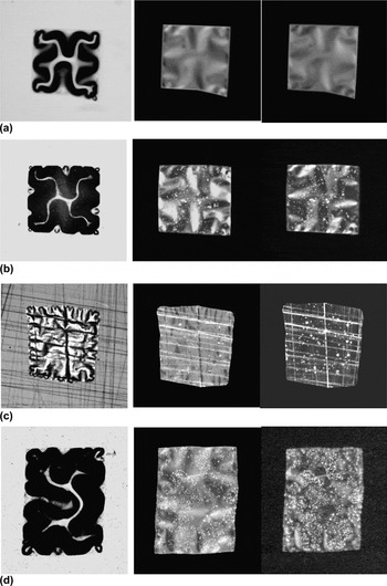
It should be emphasized that for “the first time,” the production of “self-supported amorphous SrTiO3 films” was successful by controlling (via film thickness, polycrystalline buffer layer, and roughness of substrate) the initial stress magnitude in as-deposited film. Figure 8 represents the postannealed s-s STO films prepared from amorphous clamped films (thickness 400 nm) that were sputtered on the treated surface of Si. A marked difference can be perceived in the buckled patterns and structures of amorphous and partially crystalline s-s STO films in comparison with s-s BTO films sputtered on smooth surfaces (see Figs. 6 and 8).
Optical images in reflected and transmitted cross-polarized light (with different direction of the light polarizer and analyzer) of s-s STO films after 520 °C: (a) amorphous and (b–d) partially crystalline.

IV. STRAIN-ARRANGED AMORPHOUS FILM
Understanding the processes that give rise to strain-arranged structure in amorphous films makes it possible to clarify and discuss an alternative approach to interpretation of the basic regularities in the films.
A. Surface roughness and buffer layer
To avoid film fractures and preserve the film’s amorphous nature, the adhesion energy (level of clamping) should be controlled from the very beginning of the deposition process. The use of diverse materials for the substrate or buffer layer can lead to insignificant stress changing, due to the thermal expansion mismatch between film and substrate. However, “the surface roughness” of the substrate or polycrystalline buffer layer, as a rule, significant decreases the stress value. In fact, a variety of materials can be used as a substrate, provided that they have acquired an appropriate roughness that is optimal way to master the adhesion level. Sufficient roughness can be introduced either by chemical and plasma etching, by lithography, or by the abrasive machining as in the current work. Such treatment influences not only the adherence but also the type and value of stress in the as-deposited film.
B. Nucleation and crystallization of strained amorphous film
1. Clamped films
The crystallization of highly stressed clamped film takes place “only” with stress abatement to much smaller magnitude, and it is rare for a condition favorable to crystallization to arise [Figs. 2(d) and 4(d)]. The nucleation in a stressed clamped film is retarded by high stress magnitude.Reference Sokol, Kosevich and Givargizov18
2. Self-supported film
Stress in s-s films is relieved mainly via buckling, giving rise to inhomogeneous distribution of domains differing in density, curvature, and stress. During postannealing, the growing with temperature stress abates differently depending on the domain’s local conditions. As a result, both crystalline and amorphous domains may coexist in the annealed s-s film.
The crystalline areas have random crystallite orientation. The basis for this statement comes from readings of XRD measurements of 24 s-s BTO films annealed at 570 °C (among them were amorphous, partially crystalline, and fully crystalline films) obtained by using the x-rays microbeam from a SR sourceReference Feldman, Lyahovitskaya, Leitus, Lubomirsky, Wachtel, Bushuev, Vaughan, Barkay and Rosenberg14(168 XRD patterns from each film). The (24 × 168) XRD SR patterns were analyzed and any of pattern could belong to the area with the crystallites of close orientations was found.
The crystallization of amorphous strained areas in s-s film can be caused by multiple heating of the film [see Figs. 3(b)–3(f) in Ref. Reference Lyahovitskaya, Feldman, Zon, Wachtel, Lubomirsky and Roytburd19]. Presumably, the crystallization by the multiple laser illumination during pyroelectrical measurements of s-s films can lead to degradation of the film’s properties.
C. Physical properties
The piezo- and pyroelectricity in amorphous BTO and STO films are conditioned by formation of the strain-arranged structure of elastic domains. These properties depend strongly on the clamping level and plastic properties of the amorphous material. It is generally known that the film’s clamping diminution enhances piezo- and pyroelectricity. According to our experience in clamped film STO deposited on a rough surface, the significant enhancement of the pyro-and piezoelectricity was detected.
The super-pyroelectricity of s-s BTO films is conditioned, probably, by the lack of clamping and presence of strained arranged amorphous areas.
D. Oriented growth on strain-arranged amorphous film
The amorphous materials have a broad range of applications in thin film engineering including the oriented crystallization on amorphous substrates.Reference Givargisov20 The strain-arranged amorphous films could have an application as substrates for oriented film crystallization/recrystallization. The theoretical prerequisite and experimental confirmation of orienting action of the substrate anisotropic stresses presented in Ref. Reference Bityurin, Gaponov, Gudkov and Mironov21 serve as evidence of this statement. The solid-phase recrystallization of S deposited on single-crystal LiNbO3and the nucleation of PbTe thin films were studied. In the last case, the anisotropic strain of the substrate arising from the laser irradiation through the different masks patterns induces the preferential growth of crystallites of definite (correlated with mask pattern) orientation (100) or (111).Reference Bityurin, Gaponov, Gudkov and Mironov21
Let us assume that the orienting action of stresses operates in water crystallizationReference Ehre, Lavert, Lahav and Lubomirsky22 leading to different crystallites orientation in a variety of ways on the treated surface of strained amorphous substrates.
V. CONCLUSION
The major factor determining the steady state of the amorphous films is the film/substrate adhesion energy (level of clamping). The stress value in as-deposited films depends on the clamping level and the level should be controlled from the very beginning of the deposition process. The initial stress in turn defines the specific mode of stress relief in the film. If the stress magnitude is high, stress abatement is achieved via plastic transformation resulting in stress redistribution and formation of “the strain-arranged structure of elastic domains.” If the stress magnitude is too high and exceeds the elastic limit of the material, the stress may be relaxed via development of cracks or rupture of the film. At much smaller magnitude, the stress is relieved largely by crystallization.
Contrary to their crystalline counterparts, amorphous films can accommodate stress without corruption at much higher thicknesses. This is due to the difference in mechanisms of plastic deformation in amorphous and crystalline phases. Indeed, clamped stressed amorphous films hundreds of nanometer thick are rather common, while undamaged stressed crystalline BTO films thicker than a few nm4are rarely observed. Owing to the elasticity, the s-s amorphous BTO films have a large value of volume expansion with temperature.Reference Ebralidze, Lyahovitskaya, Zon, Wachtel and Lubomirsky17
The amorphous films with arranged elastic domains could be used as the substrates for oriented crystallization and oriented recrystallization.
The successful production (by RF sputtering and e-beam deposition) via controlled substrate engineering of the strain-arranged amorphous films of BTO, STO, and SRO and the amorphous films of certain metals and oxides on the various substrates (including the use nanotubes as a “rough substrate”) is the experimental verification of the proposed conception.
ACKNOWLEDGMENTS
We thank Dr. G. Leitus for useful discussions, Dr. H. Cohen for the XPS measurement, and Dr. K. Gartsman for the SEM investigation. V.L. would like to thank Dr. Yu. Rosenberg for many important comments and discussions. This work received financial support from Prof. R. Tenne (Weizmann Institute of Science). AIF acknowledges the support of the U.S. DOE Grant No. DE-FG02-03ER15476. Beamline X18B at the NSLS is supported in part by the Synchrotron Catalysis Consortium, U.S. DOE Grant No. DE-FG02-05ER15688.