Introduction
Robust performances of advanced structural materials under extreme conditions play an important role in the design of next-generation nuclear reactors [Reference Mansur, Rowcliffe, Nanstad, Zinkle, Corwin and Stoller1, Reference Zinkle and Busby2, Reference Allen, Busby, Meyer and Petti3, Reference Zinkle and Was4]. Enhanced radiation tolerance can be achieved through tailoring inherent material properties [Reference Zhang, Stocks, Jin, Lu, Bei, Sales, Wang, Béland, Stoller and Samolyuk5] and introducing interfaces [Reference Beyerlein, Caro, Demkowicz, Mara, Misra and Uberuaga6]. Nanostructured materials, such as oxide dispersion–strengthened alloys [Reference Odette, Alinger and Wirth7, Reference Aydogan, Almirall, Odette, Maloy, Anderoglu, Shao, Gigax, Price, Chen and Chen8, Reference Chen, Aydogan, Gigax, Chen, Wang, Wang, Ukai, Garner and Shao9, Reference Edmondson, Parish, Li and Miller10], nanocrystalline alloys [Reference El-Atwani, Hattar, Hinks, Greaves, Harilal and Hassanein11, Reference Yu, Liu, Sun, Wang, Shao, Fu and Zhang12], nanotwinned metals [Reference Chen, Li, Yu, Wang, Kirk, Li and Zhang13, Reference Fan, Li, Fan, Wang and Zhang14], and nanolaminated materials [Reference Jiao, Chen, Myers, General, Shao, Zhang and Wang15, Reference Kim, Jiao, Khatkhatay, Martin, Lee, Shao, Zhang, Swadener, Wang, Gan, Cole and Wang16, Reference Yu, Sun, Chen, Liu, Wang, Kirk, Li and Zhang17, Reference Chen, Li, Yuryev, Baldwin, Wang and Demkowicz18], contain abundant interfaces, which can serve as effective defect sinks to absorb irradiation-generated defects and relieve radiation damage [Reference Zhang, Hattar, Chen, Shao, Li, Sun, Yu, Li, Taheri, Wang, Wang and Nastasi19]. Hattar et al. [Reference Hattar, Demkowicz, Misra, Robertson and Hoagland20] showed that He bubble size can be limited in immiscible Cu/Nb nanolayers. Misra et al. [Reference Misra, Demkowicz, Zhang and Hoagland21] showed that Cu/Nb layer interfaces curtail the nucleation and growth of He bubbles. Bulk Cu/Nb nanocomposites can be fabricated by accumulated roll bonding (ARB), and He cavities preferentially form along layer interfaces similar to nanolayered films [Reference Han, Mara, Wang, Misra and Demkowicz22]. The strategies of utilizing layer interfaces to trap defect clusters and alleviate radiation damage have also been reported in other systems, such as Cu/V [Reference Fu, Misra, Wang, Shao and Zhang23, Reference Fu, Carter, Swadener, Misra, Shao, Wang and Zhang24], Al/Nb [Reference Li, Martin, Anderoglu, Misra, Shao, Wang and Zhang25], Cu/Mo [Reference Li, Carter, Misra, Shao, Wang and Zhang26], Ag/Ni [Reference Yu, Liu, Fu, Wang, Myers, Wang, Shao and Zhang27], and Fe/W [Reference Li, Fu, Wang, Carter, Shao, Maloy, Misra and Zhang28]. Generally, the reduction in layer thickness leads to enhanced radiation performance due to the increasing density of layer interfaces.
Most prior studies focus on nanolaminated materials containing crystalline/crystalline (C/C) interfaces. The study on radiation response of crystalline/amorphous (C/A) nanolaminates is scarce. Zhang et al. [Reference Zhang, Wang, Liang, Zeng, Liu and Sun29] showed size-dependent radiation tolerance of Cu/amorphous-CuZr nanolaminates against He implantation. Yu et al. [Reference Yu, Fan, Chen, Song, Liu, Wang, Kirk, Li and Zhang30] showed that irradiation-induced Fe/amorphous-FeZr interfaces could absorb defects and confine the movement of dislocation loops in crystalline layers to annihilate opposite defects under in situ Kr ion irradiation. Chen et al. [Reference Chen, Jiao, Sun, Song, Yu, Liu, Kirk, Li, Wang and Zhang31] discovered that nanocrystallization in Fe/amorphous-Y2O3 nanolaminates is size dependent under Kr ion irradiation. However, questions such as irradiation-induced grain growth, phase stability of amorphous layers, and effects of C/A interfaces on radiation tolerance remain to be elucidated further.
On the other hand, it has been shown that C/A interfaces can effectively enhance the mechanical properties of bulk- and thin-film metallic glass composites [Reference Hofmann, Suh, Wiest, Duan, Lind, Demetriou and Johnson32, Reference He, Löser, Eckert and Schultz33, Reference Fan, Li, Yang, Wang, Li, Xue, Wang, Lou and Zhang34, Reference Wang, Li, Hamza and Barbee35, Reference Lee, Li and Schuh36, Reference Kim, Jang and Greer37, Reference Fan, Xue, Wang, Yu, Wang and Zhang38, Reference Wu, Xiao, Chen, Liu and Lu39]. Investigations of radiation response of C/A nanolaminates may potentially pave the way for their applications in radiation environments. Here, we report an in situ study of Cu/amorphous-CuNb (referred as Cu/a-CuNb hereafter) nanolaminates with varying individual layer thickness (h) under Kr ion irradiation. We show that accompanied with compositional segregation in a-CuNb layers, nanocrystals and nanotwins can form in nanolaminates with h of 100 nm, but nanocrystallization is significantly reduced when h is 10 or 50 nm. Grain coarsening is observed in crystalline Cu layers and is size dependent. Moreover, C/A interfaces are stable during irradiation and act as effective sinks to absorb defect clusters with little morphological changes.
Results
Irradiation-induced nanocrystallization
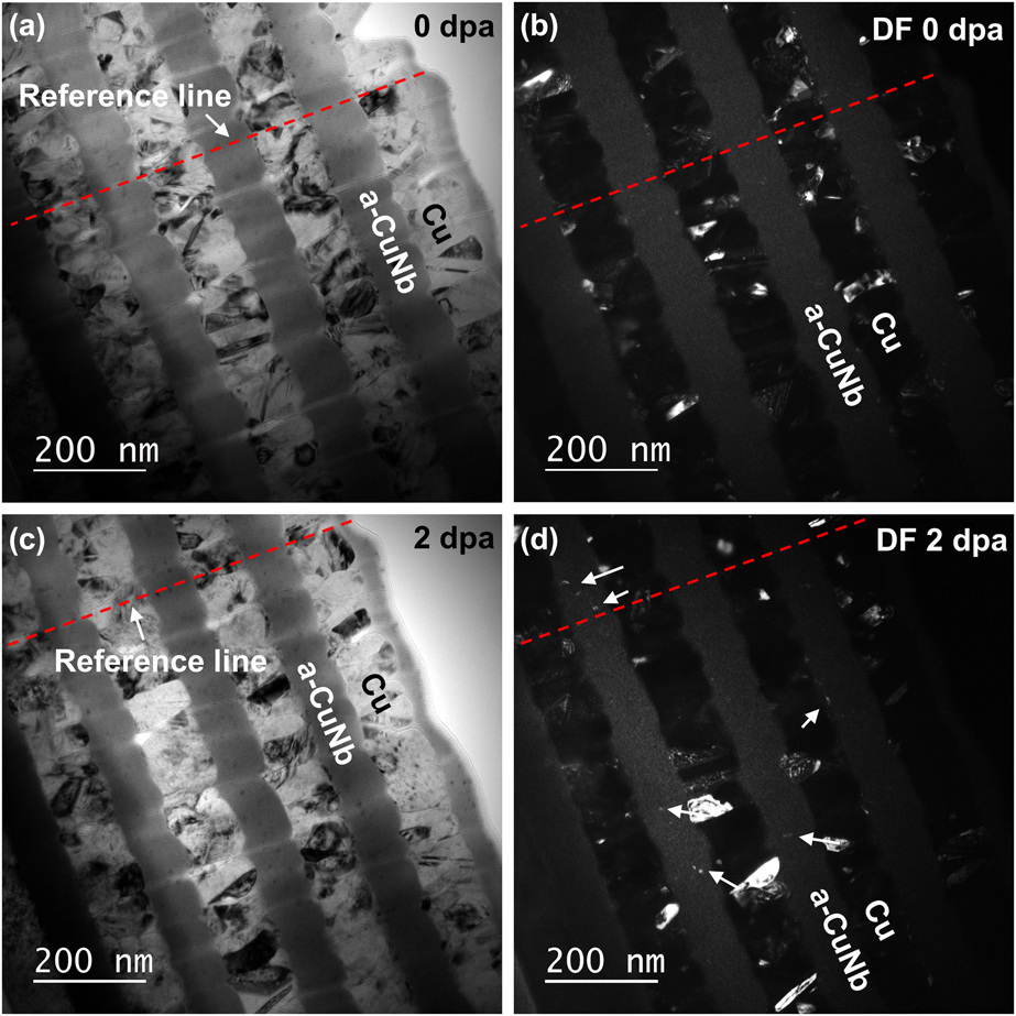
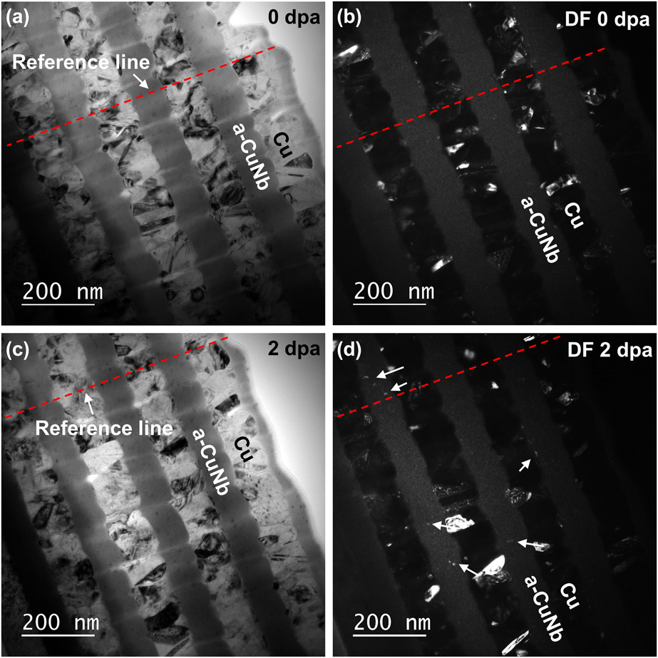
Bright-field (BF) and dark-field (DF) transmission electron microscopy (TEM) images in Figs. 1(a) and 1(b) show the nanocrystalline Cu and fully amorphous CuNb in the as-deposited Cu/a-CuNb 100-nm nanolaminates. Nanocrystals formed in a-CuNb after in situ Kr ion irradiation to 2 dpa, as indicated by the arrows in Fig. 1(d). The dashed reference line indicates the same position of the sample.
Irradiation-induced formation of nanocrystals in Cu/a-CuNb 100-nm nanolaminates. (a, b) BF and DF cross-section TEM images of as-deposited specimens (0 dpa). (c, d) BF and DF cross-section TEM images after irradiation to 2 dpa. Nanocrystals formed in a-CuNb layers after irradiation are marked by arrows. The red dashed lines indicate the reference position.
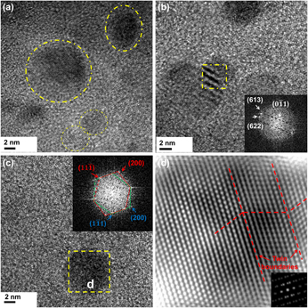
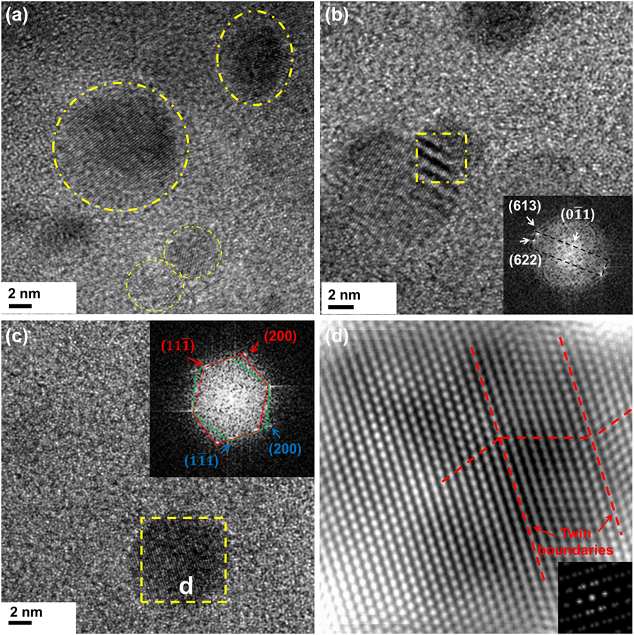
Irradiation-induced nanocrystals in a-CuNb were then characterized by high-resolution TEM. The size of nanocrystals ranges from 5 to 10 nm, as indicated by the circles in Fig. 2(a). The fast Fourier transform (FFT) with crystalline dots in Fig. 2(b) comes from the Nb crystal of irregular shape. The FFT in Fig. 2(c) is from the dashed box and shows the diffraction dots of typical twin structure from the Cu nanocrystal. Figure 2(d) shows the HRTEM image of the twinned Cu nanocrystal.
Nanocrystals and nanotwins observed in high-resolution TEM (HRTEM) images of Cu/a-CuNb 100-nm nanolaminates after irradiation to 2 dpa. (a) Nanocrystals of spherical shape marked by the dashed circles in HRTEM image. (b) An irregular shape Nb nanocrystal marked by a dashed box whose FFT is shown in the inset. (c) A twinned Cu nanocrystal formed in irradiated a-CuNb. The inset FFT confirms the twinned structure. (d) HRTEM of dashed box in c shows the irradiation-induced nanotwin.
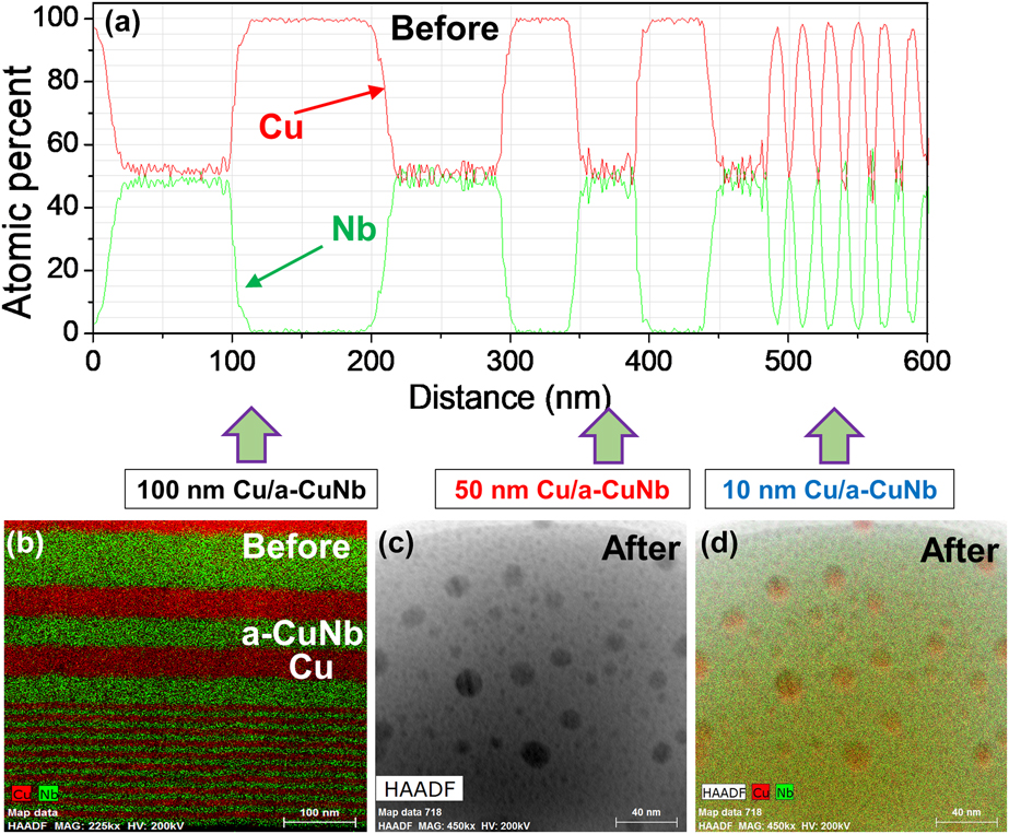
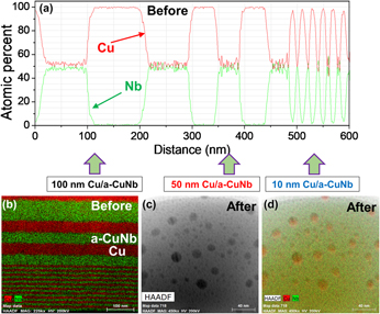
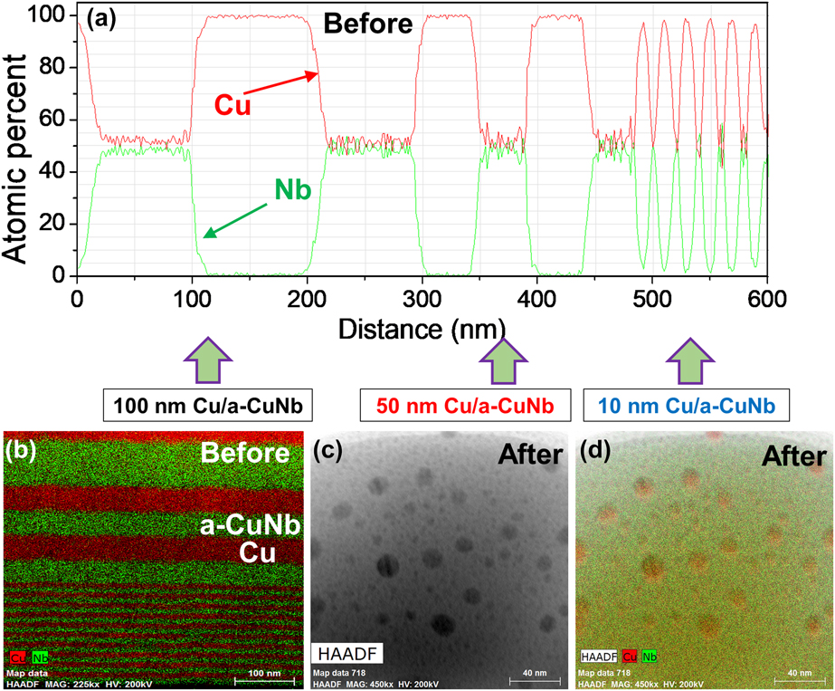
EDS composition profile of Cu/a-CuNb nanolaminates with varying h is shown in Fig. 3(a), and no element segregation was observed before irradiation [Fig. 3(b)]. However, after irradiation to 5 dpa, Cu-enriched particles from several to tens of nanometers can be identified in the a-CuNb matrix [Figs. 3(c) and 3(d)].
Composition profile of Cu/a-CuNb nanolaminates and single-layer a-CuNb before and after irradiation. (a) Line scan profile of Cu/a-CuNb nanolaminates with varying h before irradiation. (b) EDS map of Cu/a-CuNb nanolaminates with varying h before irradiation. (c) HAADF image of single-layer a-CuNb after irradiation. (d) EDS map of (c) shows the formation of Cu-enriched particles inside the amorphous matrix after irradiation to 5 dpa.
Evolution of grain boundary and layer interface during irradiation
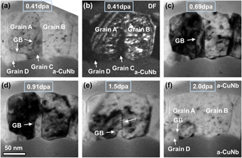
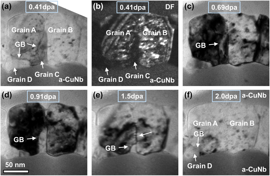
Grain boundary (GB) migration was observed during in situ radiation in Cu/a-CuNb 100-nm nanolaminates. As shown in the snapshots in Fig. 4 (details can be found in Supplementary material video 1), a small grain C existed between two larger grains, A and B. The GB between grain A and C gradually migrated with the increase of dose. During its migration, the GB actively interacted with defect clusters, and eventually grain C contracted and disappeared, leaving behind grains A and B. Besides, GB between grain A and D also migrated during the process, and the GB migration led to the shrinkage of grain D.
GB migration shown by in situ TEM snapshots during irradiation of Cu/a-CuNb 100-nm nanolaminates. (a, b) BF and DF TEM micrographs showing grain C between grain A and B. (c–e) GB migration during irradiation (0.69–1.5 dpa). (f) Removal of grain C as a result of GB migration. Detailed information can be found in the Supplementary material video 1.
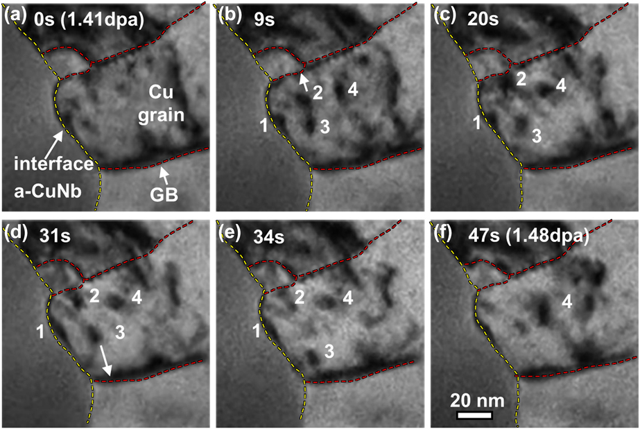
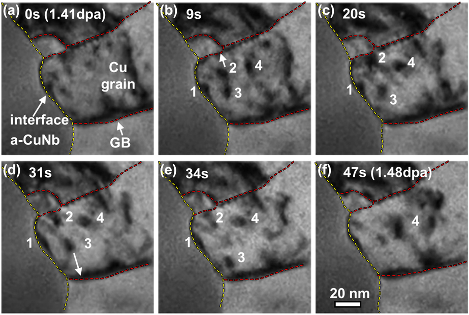
Interactions of defect clusters with layer interfaces were observed during irradiation as shown in Fig. 5 (See Supplementary material video 2). Defect cluster 1 at one layer interface was gradually absorbed by the interface. No significant morphological change of the interface could be observed. During radiation, defect clusters 2 and 3 migrated toward opposite GBs and were readily absorbed by the GBs. Defect cluster 4 away from interface and GBs changed its morphology but remained in the grain during radiation.
Defect absorption by GB and crystalline/amorphous layer interface shown by the in situ TEM snapshots during irradiation of Cu/a-CuNb 100-nm nanolaminates. (a–f) Defect cluster 1 was gradually absorbed by layer interface (yellow dashed line); defects 2 and 3 were absorbed by grain boundaries (red dashed lines), while defect 4 remained after irradiation. Detailed information can be found in Supplementary material video 2.
Layer thickness effect in grain coarsening and defect absorption
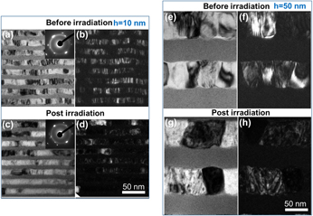
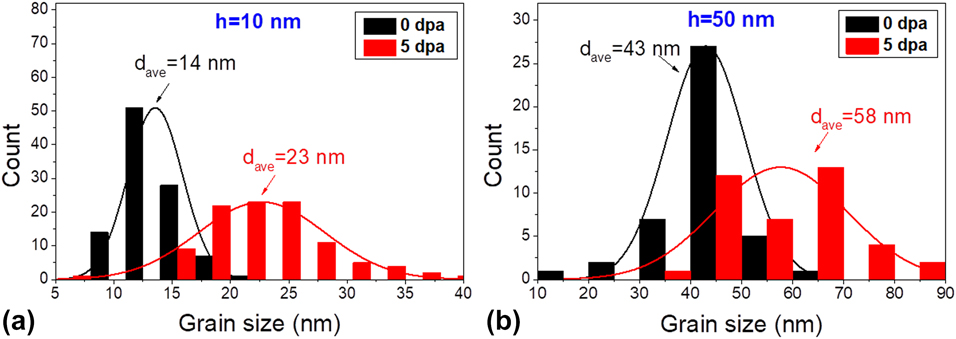
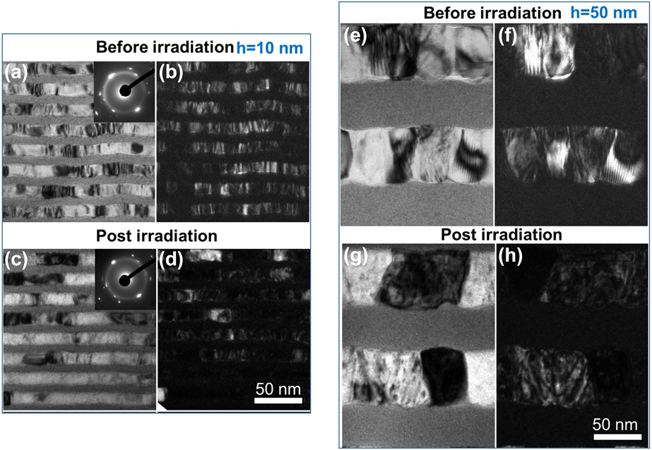
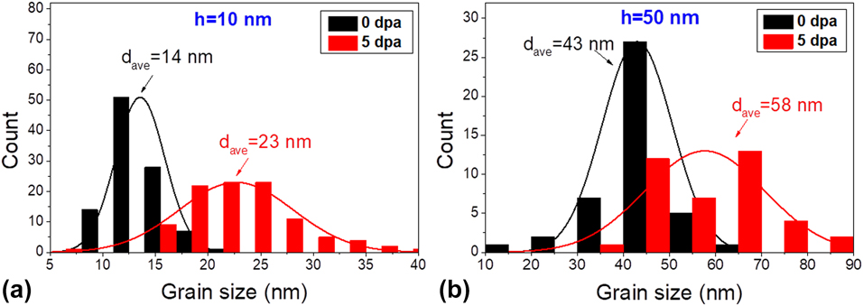
TEM images of Cu/a-CuNb 10 and 50-nm nanolaminates before and after irradiation are compared in Fig. 6. Before irradiation, the grain size of Cu is similar to h, consistent with the previous study [Reference Fan, Liu, Xue, Rahimi, Bahr, Wang and Zhang40]. After irradiation to 5 dpa, the grain size of both multilayer systems increased and grain coarsening was more prominent in the Cu/a-CuNb 10-nm nanolaminates. Grain size was calculated as the diameter measured from projection area of grains in TEM images. Comparison of Cu grain size distributions in Fig. 7 shows that for Cu/a-CuNb 10-nm nanolaminates, the average Cu grain size increases by 67% from 14 to 23 nm, whereas the average Cu grain size in the Cu/a-CuNb 50-nm nanolaminates increases moderately from 43 to 58 nm (∼34% increase).
Comparison of microstructure of Cu/a-CuNb 10 and 50-nm nanolaminates before and after irradiation. (a–d) BF and DF TEM images showing grain coarsening in irradiated Cu/a-CuNb 10-nm nanolaminates. (e–h) Grain growth was also observed in irradiated Cu/a-CuNb 50-nm nanolaminates.
Cu grain size distribution before and after irradiation to 5 dpa for (a) Cu/a-CuNb 10-nm and (b) Cu/a-CuNb 50-nm nanolaminates. The average grain size of Cu increases from ∼14 to 23 nm (∼67% increase) for the irradiated Cu/a-CuNb 10-nm nanolaminates and increases from ∼43 to 58 nm (∼34% increase) for the Cu/a-CuNb 50-nm nanolaminates.
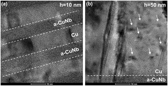
In the irradiated Cu/a-CuNb 10-nm nanolaminates, very few defect clusters remained in Cu layers [Fig. 8(a)]. In contrast, the Cu layers in the irradiated Cu/a-CuNb 50-nm nanolaminates contained abundant defect clusters and stacking faults [Fig. 8(b)].
Defect morphology after irradiation of (a) Cu/a-CuNb 10-nm and (b) Cu/a-CuNb 50-nm nanolaminates in TEM images. After irradiation, the grain interior of Cu/a-CuNb 10 nm contained few defect clusters, whereas for the irradiated Cu/a-CuNb 50 nm, abundant defect clusters and stacking faults existed in Cu layers.

Discussion
The formation of nanocrystals and nanotwins in irradiated amorphous-CuNb layers
It has been shown that nanocrystals and nanotwins embedded in certain amorphous alloys (or the so called metallic glasses) can substantially improve the mechanical properties of amorphous composites [Reference Chen, Inoue, Zhang and Sakurai41, Reference Pauly, Gorantla, Wang, Kühn and Eckert42]. Various types of radiation techniques have been used to introduce nanocrystals in amorphous alloys, such as electron irradiation [Reference Nino, Nagase and Umakoshi43, Reference Nagase, Nakamura and Umakoshi44, Reference Fu, Carter, Martin, Xie, Zhang, Wang, Littleton and Shao45, Reference Xie, Zhang, Louzguine-Luzgin, Zhang and Inoue46, Reference Tarumi, Takashima and Higo47], heavy ion irradiation [Reference Brimhall48, Reference Luo, Yang and Chen49, Reference Carter, Fu, Martin, Xie, Zhang, Wang, Wijesundera, Wang, Chu and Shao50, Reference Myers, Charnvanichborikarn, Wei, Luo, Xie, Kucheyev, Lucca and Shao51], and helium irradiation [Reference Xie, Shao, Louzguine-Luzgin and Inoue52, Reference Carter, Fu, Bassiri, Dvorak, Theodore, Xie, Lucca, Martin, Hollander and Zhang53]. However, generally the elements in the amorphous alloys are miscible and the irradiation-induced nanocrystals usually contain multiple elements. For example, Fu et al. [Reference Fu, Carter, Martin, Xie, Zhang, Wang, Littleton and Shao45] showed that crystalline Cu10Zr7 phases formed in amorphous Cu50Zr45Ti5 under 200-keV electron irradiation. Since the composition of nanocrystals is not significantly different from the composition of the amorphous matrix in the prior studies, substantial compositional segregation may not be required for nanocrystal formation. However, in our work, Cu and Nb in a-CuNb layers have a positive heat of mixing, 3 kJ/mol [Reference Takeuchi and Inoue54]. Consequently, substantial compositional change in the form of phase segregation is necessary for nanocrystallization during irradiation. For a-CuNb studied in this work, 200-keV electron beam irradiation under TEM did not lead to nanocrystal formation. Under 1-MeV Kr ion irradiation, nanocrystals and nanotwins formed in Cu/a-CuNb 100-nm nanolaminates, but not observed in the multilayer systems with h of 10 and 50 nm.
Upon irradiation, atoms in the amorphous matrix acquire extra kinetic energy to migrate, and irradiation can enhance the diffusion and segregation of Cu and Nb atoms. In addition, displacement cascades and subcascades due to heavy ion bombardment create a large amount of vacancies and interstitials in crystalline materials. In the case of amorphous alloys, excess free volume can be generated during ion bombardment. The excess free volume not only assists the diffusion of atoms but also serves as nucleation sites for crystallization. Due to radiation-enhanced diffusion in immiscible a-CuNb layers, substantial compositional segregation occurred as shown in the EDS map in Fig. 3. Facilitated with enhanced diffusion and compositional segregation, nanocrystals and nanotwins can be nucleated and formed in the amorphous matrix. Once formed, they will remain stable since these nanocrystals and nanotwins are energetically more favorable than metastable amorphous phase. The HRTEM images in Fig. 2 demonstrated crystalline lattices of nanocrystals and nanotwins in amorphous matrix. It is intriguing to see nanotwins formed in a-CuNb layers. Without high-resolution in situ TEM radiation, real-time formation mechanism of nanotwins cannot be uncovered. We speculate there are two possible nanotwin formation processes in the amorphous matrix. The first process involves the formation of isolated nanocrystal and their coalescence to form the nanotwinned structure. This mechanism has been demonstrated in the formation of Ag crystals by annealing [Reference Courty, Henry, Goubet and Pileni55]. On the other hand, a nanocrystal can be sheared and transformed to twinned crystal due to the lattice strain. Yu et al. [Reference Yu, Chen, Li, Liu, Wang, Kirk, Li and Zhang56] showed grain rotation in nanocrystalline metals due to Kr irradiation–induced in-plane strain. Since it is hard for crystals embedded in amorphous matrix to rotate, they could undergo shear deformation to accommodate irradiated-induced strain, which may result in deformation twins. Irradiation-induced formation of nanotwins and nanocrystals may provide an alternative route to introduce second phases in amorphous matrix to improve the mechanical properties of amorphous alloys.
Defect absorption by GB and crystalline/amorphous interface
Both GBs and C/A interfaces are effective defect sinks and contain excess free volume. Comparison of defect interaction with GB and C/A interface is shown in Fig. 5. If defects are far away from GB or C/A interfaces as the case for defect cluster 4, they are more likely to survive over a longer period of radiation. But when defect clusters (2 and 3) are in close proximity to GBs, they can be annihilated quickly. In contrast, absorption of defect clusters by C/A interfaces is a relatively sluggish process as evidenced by the gradual absorption of defect clusters along the interface observed during in situ radiation. This difference might arise from the inherently different natures between two types of boundaries. GBs are interfaces between two crystals with different crystallographic orientations, while C/A interfaces are phase boundaries between crystalline and amorphous phases, where both chemistry and lattice continuity are not maintained. GBs can effectively interact and absorb defects. Sun et al. [Reference Sun, Song, Yu, Chen, Kirk, Li, Wang and Zhang57] showed that defect clusters can be rapidly absorbed by high-angle GBs in nanocrystalline Ni, and dislocation segments in contact with these GBs in Ni can be gradually absorbed by the GBs. Bai et al. [Reference Bai, Voter, Hoagland, Nastasi and Uberuaga58] showed that the irradiated GBs are interstitial loaded and they can reemit interstitials back to the grain interior to annihilate vacancies to promote recombination. El-Atwani et al. [Reference El-Atwani, Nathaniel, Leff, Hattar and Taheri59] showed that the absorption of defect clusters by GBs depends on the misorientation angles between grains. Tschopp et al. [Reference Tschopp, Solanki, Gao, Sun, Khaleel and Horstemeyer60] have used molecular statics simulations to show that misorientation angle and GB energy are both correlated with the sink strength of GBs in Fe. Chen et al. [Reference Chen, Wang, Chen and Shao61] showed that stress field and defect formation energy minima on GBs play an important role in point defect absorption by GBs through MD simulations.
But C/A interfaces separating chemically and crystallographically different phases are quite different from conventional high-angle GBs. It is likely that defect absorption by C/A interface is a diffusion-controlled process. For instance, when a dislocation loop generated in Cu is in contact with C/A interface, the excess free volume at the C/A interfaces may allow the gradual absorption of dislocation loops by local rearrangement of atomic clusters in a-CuNb. Such a gradual defect capture/absorption process may not lead to significant morphological changes during defect-interface interactions at least under the radiation conditions explored in this study.
The movement of GBs observed during in situ radiation in Cu layers also contributes to the removal of defect clusters. As shown in the in situ snapshots of Fig. 4, GB between Grain A and C started to migrate from the point with the highest curvature as a result of chemical potential gradient. The chemical potential along surface can be expressed as follows [Reference Voorhees62, Reference Rhines, Craig and DeHoff63]:
 $$\mu = {\mu _{\rm{o}}} + {V_{\rm{m}}}\gamma k\quad ,$$
where k is the mean interfacial curvature, μo is the chemical potential of atoms at a flat interface, V m is the molar volume, and γ is the surface energy. Equation (1) shows that atoms will flow from regions of large curvature to small curvature as confirmed by the GB migration shown in Fig. 4. During its migration, the GB actively interacts with and annihilates defect clusters along its path. Consequently, the shape and structure of the GB changes during defect-GB interactions. The migration and elimination of grain C during in situ radiation is analogous to Ostwald ripening process, and grain coarsening during irradiation is facilitated by radiation-enhanced diffusion and defect-GB interactions. The high-density interfaces including both GBs and C/A phase boundaries in C/A nanolaminates lead to efficient defect absorption and enhance their radiation tolerance, and the effects of grain size and layer thickness are discussed below.
Size effect on the radiation response of Cu/a-CuNb nanolaminates
Prior studies show that h greatly affects the radiation tolerance of C/C nanolaminates, but size effect on radiation response of C/A nanolaminates is rarely studied. In our study, size effect is manifested in three ways: nanocrystallization in amorphous matrix, grain coarsening in Cu, and defect absorption in crystalline Cu layers. First, as stated in the previous section, nanocrystals or nanotwins were observed in the Cu/a-CuNb 100-nm nanolaminates but not in 10- or 50-nm nanolaminates. Nanocrystallization in a-CuNb layers requires radiation-enhanced diffusion and the assistance of radiation-induced extra free volume. But in nanolaminates with smaller h, a higher density of GBs and C/A interfaces can efficiently remove point defects induced by radiation and decrease the excess free volume generated in the amorphous layer. Consequently, the chance of forming nanocrystals is reduced. Therefore, nanocrystals are more likely to be observed in Cu/a-CuNb nanolaminates with larger h. Similar size-dependent crystallization phenomenon has been observed during in situ radiation of Fe/amorphous-Y2O3 nanolaminates [Reference Chen, Jiao, Sun, Song, Yu, Liu, Kirk, Li, Wang and Zhang31]. The critical layer thickness below which nanocrystal formation is suppressed may be affected by chemical composition, processing history, radiation dose, and sink strength of interface, and such a hypothesis is worthy of future investigations.
Second, grain coarsening in Cu is more obvious in irradiated Cu/a-CuNb nanolaminates with smaller h (Figs. 6 and 7). The underlying reasons can be 2-fold. Nanolaminates with smaller h have larger GB curvature and greater GB energy due to smaller grain size. Both factors provide larger driving force for GB migration. Furthermore, defect clusters confined in crystalline layers with smaller h interact more frequently with GBs and thus facilitate the grain coarsening process. Therefore, more substantial grain coarsening is anticipated in C/A nanolaminates with smaller h.
Third, after irradiation, grain interiors contain less defect clusters in C/A nanolaminates with smaller h, as shown in Fig. 8. The size-dependent variation of defect density should be attributed to the high density of GBs and C/A interfaces. The sink strength of GB and C/A interface can be estimated by the following equations [Reference Zhang, Hattar, Chen, Shao, Li, Sun, Yu, Li, Taheri, Wang, Wang and Nastasi19]:
 $$k_{{\rm{gb}}}^2 = {{15} / {{d^2}}}\quad ,$$
 $$k_{\rm{h}}^{\rm{2}} = {{12\eta } / {{h^2}}}\quad .$$
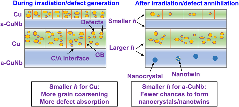
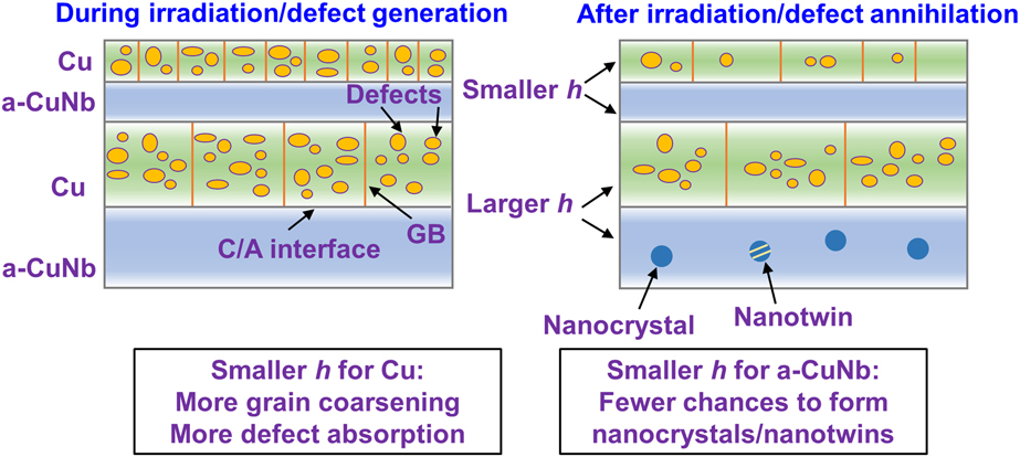
where d is the grain size and η is the sink efficiency. For incoherent and immiscible interfaces like C/A interface, η may be large. As shown in Eqs. (2) and (3), the sink strength is inversely proportional to h 2 and d 2. The increased sink strength with reducing h and d can greatly relieve radiation damage by absorbing defects through GBs and C/A interfaces. Although the density of GBs would decrease due to irradiation-induced grain coarsening, C/A interfaces are stable during radiation and remain as effective defect sinks with little morphological change under the irradiation conditions explored in this study. The effects of grain size and layer thickness can be summarized in Fig. 9. In short, smaller d and h for crystalline layers leads to more grain coarsening and more defect absorption, but smaller h for amorphous layers can potentially result in fewer chances to form nanocrystals. Therefore, to maintain the structural stability of C/A nanolaminates under irradiation without compromising defect absorption, C/A nanolaminates with thinner amorphous layers and relatively thicker crystalline layers may be desired. Prior studies suggest that nanocrystals in amorphous layers may potentially toughen C/A nanolaminates [Reference Zhang, Liu and Sun64, Reference Zhang, Liu and Sun65]. Thus, crystalline/amorphous nanolaminates with well-designed layer thickness and thickness ratio may be desirable to achieve a combination of good mechanical properties and radiation tolerance.
A schematic illustrating the grain size and layer thickness effect on grain coarsening, defect absorption, and nanocrystal formation.
Conclusions
Radiation response of crystalline Cu/amorphous-CuNb nanolaminates was studied by performing in situ Kr ion irradiation under TEM. Nanocrystals and nanotwins formed in the amorphous CuNb layers in Cu/a-CuNb 100-nm nanolaminates, but were largely absent in thinner nanolaminates. Radiation-enhanced diffusion process promotes composition segregation and the formation of nanocrystals. Absorption of defects by grain boundaries and crystalline/amorphous layer interfaces were captured by in situ studies and compared. Both stationary and migrating grain boundaries trap and annihilate defect clusters. Layer interfaces can effectively absorb defects without obvious microstructural change. Furthermore, Cu/a-CuNb nanolaminates with smaller layer thickness absorb defects more effectively and also experience more obvious grain coarsening in Cu layers. This study demonstrates size-dependent radiation response of crystalline/amorphous nanolaminates and may provide insights to the enhanced radiation tolerance of nanolayered metallic glass nanocomposites.
Experimental methods
Alternating crystalline Cu and a-CuNb layers were deposited by direct current magnetron sputtering on silicon substrate. The a-CuNb layer was co-sputtered with equal at.% of Cu and Nb. Base pressure was better than 1 × 10⁻⁷ torr, and 1–3 × 10⁻³ torr Ar was used during deposition. Two sets of nanolaminates were chosen for in situ radiation studies: Cu/a-CuNb 100-nm nanolaminates with equal h and Cu/a-CuNb nanolaminates with h varying from 10, 50, to 100 nm to study the size effect on radiation response. Single-layer a-CuNb was also irradiated as a reference. The samples for TEM characterization were prepared by mechanical grinding, polishing, and followed by ion milling. Microstructural characterization and energy-dispersive X-ray spectroscopy (EDS) chemical mapping were conducted using an FEI Tecnai G2 F20 microscope and an FEI Talos 200X TEM/STEM with ChemiSTEM (X-FEG and SuperX EDS with four silicon drift detectors) operated at 200 kV (Thermo Fisher Scientific, Hillsboro, Oregon). In situ 1-MeV Kr++ ion irradiation was conducted at room temperature at the Intermediate Voltage Electron Microscopy (IVEM) facility at Argonne National Laboratory. The microstructural evolution during irradiation was captured by a CCD camera at a frame rate of 15 frames/s. Radiation damage in displacement per atom (dpa) is calculated by SRIM with Kinch–Pease method [Reference Ziegler, Ziegler and Biersack66]. The thickness of the TEM foil is estimated to be ∼100 nm, and the dose used in this study is taken as the average dose from 0 to 100 nm in the SRIM-calculated profile for Cu. The average dose rate is 2.5 ×10⁻³ dpa/s and 1.8 × 10⁻³ dpa/s for Cu and a-CuNb layers, respectively.
Supplementary material
To view supplementary material for this article, please visit https://doi.org/10.1557/jmr.2019.24.
Acknowledgments
We acknowledge the financial support by NSF-CMMI-1728419. C. Fan is supported by the Bisland Fellowship at Purdue University. H. Wang acknowledges the support from the U.S. Office of Naval Research (N00014-16-1-2778). This work was supported by the U.S. Department of Energy, Office of Nuclear Energy under DOE Idaho Operations Office Contract DE-AC07- 051D14517 as part of a Nuclear Science User Facilities experiment. Accesses to the Life Sciences Microscopy Center and Materials Science Microscopy Center at Purdue University are also acknowledged. We also acknowledge DOE-NEUP 18-15703 for partial financial support.