I. INTRODUCTION
Growth of nanoarchitectures with a tunable dimension and structure complexity represents a challenge in the field of nanoscience and is an essential step toward the realization of multifunctionality of nanosystems.Reference Yan, He, Johnson, Law, Saykally and Yang1–Reference Matthew and Song4 In particular, one-dimensional semiconductor heterostructures have gained increasing attention in recent years because of their synergic physical properties that originate but differ from the individual constituents and, thus, are more useful for constructing new-concept nanoscale optoelectronic devices.Reference Cheng, Liu, Sie, Zhou, Zhang, Gong, Huan, Sum, Sun and Fan5–Reference Hwang, Boukai and Yang9 Currently, the typical synthetic methods for high-quality monocrystalline heterostructures are based on vapor phase epitaxial growth such as metal-organic vapor phase epitaxy and molecule beam epitaxy, which utilizes the moderate mismatches between the two different materials and involves the vapor–liquid–solid process. In contrast to the vapor phase epitaxy, solution epitaxial growth of heterostructures is of particular interest because of its simplicity of fabrication and low cost, although it is more challenging to satisfy the lower mismatche requirement.Reference Dong, Tang and Buhro10–Reference Fan, Ding, Liu, Tian and Wang12 In the past few years, various oxide semiconductor heterostructures such as SnO2/Fe2O3,Reference Zhang, Sun, Jia, Yan, You and Yan13 ZnO/TiO2,Reference Wang, Sun, Zhao, Zhou, Chen and Jiang14 and SnO2/TiO2Reference Gubbala, Chakrapani, Kumar and Sunkara15, Reference Qian, Liu, Xiao, Jiang, Cao, Ai and Yang16 have been investigated because of their wide applications. Among them, TiO2 and SnO2 are well-known wide direct-bandgap materials and possess application potential in photoelectrochemical (PEC) water splitting,Reference Feng, Shankar, Varghese, Paulose, Latempa and Grimes17 dye-sensitized solar cells,Reference O’Regan and Gratzel18 gas sensing,Reference Tan, Ho, Wong, Kawi and Wee19 and so on. It has been previously demonstrated that TiO2 coupling with SnO2 semiconductor can facilitate the charge separation and transportation because of the proper band edge alignment and higher electron mobility of SnO2 and thus boost up the photoconversion efficiency.Reference Gubbala, Chakrapani, Kumar and Sunkara15, Reference Qian, Liu, Xiao, Jiang, Cao, Ai and Yang16 Although various methods have been explored for the controlled synthesis of nanostructures of both SnO2 and TiO2 individually, a high level of structural and morphological control for the SnO2/TiO2 heterostructured nanowires has not been reported yet.
Here we report a facile synthetic route to the fabrication of dendritic SnO2/TiO2 heteronanostructures for the first time by selecting pregrown single crystalline SnO2 nanowires as the substrate for the solution epitaxial growth of TiO2 nanorod branches. The interface epitaxy, as determined from electron microscopy analysis, accounts for the twofold symmetry and the unusual growth direction of TiO2. As a proof-of-concept demonstration of their functional property, the nanostructures SnO2/TiO2 are tested as photoanode for PEC water splitting.
II. EXPERIMENTAL
A. Synthesis of SnO2–TiO2 hybrid nanowires
The SnO2 nanowires were synthesized by a standard chemical vapor deposition route following our previous publications.Reference Cheng, Liu, Yang, Zhou, Sun, Chen, Yu, Zhang, Gong, Sun and Fan20 Briefly, an equal amount of SnO2 powder (99.9%; Sigma Aldrich, St. Louis, MO) and graphite powder (99%; Sigma Aldrich, Switzerland) were grounded and transferred to an alumina boat, which was located at the center of a quartz tube furnace. Gold sputter–coated Si substrates were typically placed 1−4 cm away from the center of the boat. The temperature of the furnace was ramped to 1050 °C at a rate of 50 °C/min and kept at that temperature for 1 h under a constant flow with 50 sccm of Ar + O2 (99.5% + 0.5%) mixed gas and a pressure of 15 mbar. After the furnace cooled to room temperature, the substrate surface turned to white or light gray color, indicating the deposition of materials. For the growth of TiO2 nanobranches, the SnO2 nanowires–covered substrates were placed within a 50 mL sealed Teflon-lined stainless steel autoclave containing 25 mL of toluene, 1 mL of tetrabutyl titanate, and 1 mL of hydrochloric acid. The hydrothermal process was conducted at 180 °C for various periods from 1 min to 5 h. After the reactions, the substrates were rinsed with deionized water and dried with N2 blow.
B. Characterizations
The morphology and structures of as prepared product were characterized with a JEOL JSM-6700F field emission scanning electron microscope (FE-SEM, JEOL, Tokyo, Japan) and a JEM 2010F high resolution transmission electron microscope (HRTEM, JEOL, Tokyo, Japan). X-ray powder diffraction (XRD; Bruker AXS Inc. Karlsruhe, Germany) patterns were recorded on a Bruker D8 Advance diffractometer using Cu Kα radiation.
C. PEC water splitting measurement
The PEC characteristics of twofold symmetry SnO2/TiO2 electrodes (working area, 0.2 cm2) as photoanodes were measured using CHI 760C (CHI Instrument, Austin, TX) potentiostat in a three-electrode cell with 1 M NaOH as electrolyte using Ag/AgCl in saturated KCl as a reference electrode and Pt sheet as a counter electrode. The linear sweep voltammagram curves were obtained in 1 M NaOH in the dark or under illumination. The chronoamperometry curves were measured at 0.5 V versus Ag/AgCl. The samples were illuminated with simulated sunlight from a 150-W xenon lamp (SS150; Sciencetech Inc., London, Canada) using AM 1.5G filter with a measured intensity of 1 sun (100 mW cm−2, spectrally corrected) at the sample face.
III. RESULTS AND DISCUSSION
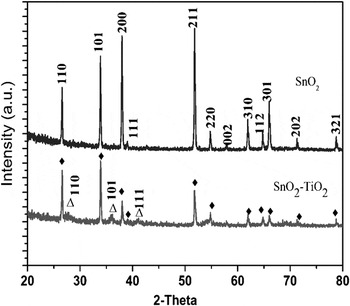
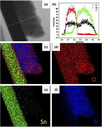
Figure 1(a) shows the typical scanning electron microscope (SEM) and transmission electron microscope (TEM) images of the primary SnO2 nanowires. The nanowires have a diameter of 40−80 nm and length of several tens of micrometers with very smooth surfaces. After the hydrothermal growth process, very dense TiO2 nanorods branched out mainly from the two side facets of SnO2 nanowire trunks, resembling a dendritic structure [Figs. 1(b) and 1(c)]. In general, the TiO2 nanorod branches assembling in a bundle structure stand with a fixed ∼70° angle to the two side surfaces of the SnO2 nanowires as multiple rows in a parallel manner, forming a twofold point symmetry. The length of the TiO2 nanorods ranges from 300 to 400 nm and the diameter of individual TiO2 nanorod is ∼10 nm. The XRD patterns obtained from the SnO2 and SnO2/TiO2 hybrid structures confirm that both SnO2 and TiO2 are tetragonal rutile phase (Fig. 2). Further compositional analysis was conducted by energy dispersive x-ray spectroscopy elemental mapping. Figure 3 shows the line scanning and elemental mapping results, which clearly illustrates that the trunk and the branches of the heterostructures are composed of pure SnO2 and TiO2, respectively.
General morphology of the nanostructure. (a) Scanning electron microscope (SEM) image of the primary SnO2 nanowires. Inset: transmission electron microscope (TEM) image of one SnO2 nanowire. (b, c) Typical SEM images of the dendritic SnO2/TiO2 nanostructures.

X-ray powder diffraction patterns of primary SnO2 nanowire backbones (top) and dendritic SnO2/TiO2 heterostructures (bottom), “♦” indicates the rutile phase of SnO2 and “∆” indicates the rutile phase of TiO2.

Composition analysis by energy dispersive x-ray spectroscopy (EDX). (a) TEM image of a single dendritic SnO2/TiO2 structure. (b) EDX line scanning along the direction indicated in (a) showing the element profile. (c)–(f) Elemental mapping images by scanning TEM.

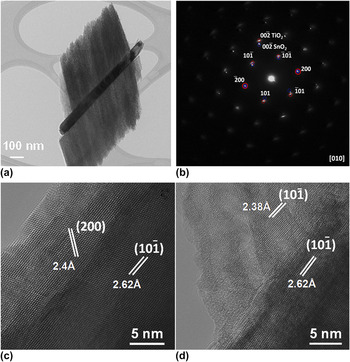
Figure 4(a) shows a typical TEM image of the SnO2/TiO2 dendrite nanorods. The quasi two-dimensional (2D) structure was tilted to allow its selected area electron diffraction pattern to be recorded in the [010] zone axis. The diffraction pattern [Fig. 4(b)] consists of two sets of clearly correlated patterns, from which one can see that both the SnO2 and TiO2 are in the same zone axis and have the same orientation, revealing the perfect interfacial lattice relationship between the two stem and branch. Further insight into the structural information was obtained by HRTEM in its [010] zone axis. On the basis of the HRTEM images taken from the SnO2 backbone [Fig. 4(c)] and the interface [Fig. 4(d)], the lattice spacings are measured to be 2.62 and 2.38 Å, which are consistent with the d-spacings of  planes of tetragonal SnO2 and
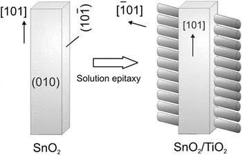
 of TiO2, respectively. From the above HRTEM and selected area electron diffraction (SAED) analysis, we can conclude that the SnO2 nanowire stems grow in the [101] direction bounded by
 and {010} surface facets. The longitudinal direction of the TiO2 branch is then determined to be along
 . The stem–branch angle determined from these reciprocal lattice peaks [Fig. 4(b)], 70.6°, is consistent with the 68° angle between the two growth directions for the stem and branch. Therefore, the adopted epitaxial orientation relationship between the stem and branch is TiO2[010]//SnO2[010] and TiO2
 //SnO2
 . The perfect alignment observed in these branch structures is reasonable considering the relatively small lattice mismatch (−0.91%) between the
 crystal plane of rutile SnO2 [lattice plane spacing d
 =2.62 Å] and TiO2 [d
 =2.38 Å]. Thus, the TiO2 nanorod branches preferably grew in the two
 side faces, but not on the other (±010) faces, of the SnO2 nanowire stems, resulting in the twofold point symmetry dendritic structure.
Crystallographic orientation by TEM investigation. (a) TEM image of one SnO2/TiO2 dendritic structure. (b) Corresponding electrion diffraction pattern recorded from the SnO2/TiO2 trunk–branch interface with the [010] zone axis. The diffraction spots from rutile SnO2 and TiO2 planes are labeled in blue and red, respectively. High resolution TEM images taken from (c) the SnO2 nanowire trunk and (d) the trunk–branch interface.

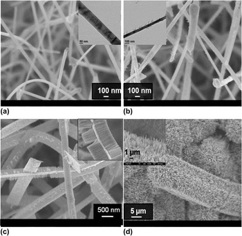
To obtain an insight of the morphology evolution of the SnO2/TiO2 dendritic nanostructures, time-dependent experiments were conducted. SEM images of the obtained nanostructure are shown in Fig. 5. With the reaction time being shorter than 1 min, there was only a sparse growth of nanorods on the surface of SnO2 nanowires; only a few tiny nanorods formed [Fig. 5(b)] because of the few initial nucleation and growth sites. Extending the reaction to 5 min resulted in the growth of very dense TiO2 nanorod branches, forming the hierarchical structures with a twofold point symmetry as we discussed earlier. When the reaction time was further increased to 5 h, the TiO2 nanorods, several micrometers long, covered the whole surface of SnO2 nanowires radially without an evident heterosymmetry [Fig. 5(d)].
Time-dependent growth of the SnO2/TiO2 dendritic nanostructures. (a) Before growth; (b) 1 min; (c) 5 min; (d) 5 h. Insets in (a) and (b) are the corresponding TEM images. Insets in (c) and (d) are the enlarged view.

The growth process is schematically shown in Fig. 6. During the initial growth process, TiO2 nanoparticles tend to nucleate onto the SnO2 side surfaces. Driven by a minimization of the lattice misfits, the rutile phase TiO2 nanoparticles are preferentially oriented along the  direction on the
 facets of SnO2 under the synthetic condition we used, which has been evidenced by HRTEM and SAED. Herein, the solution interface epitaxy is essential for the formation of the dendritic nanostructures with a twofold point symmetry. It is noteworthy that the preferential growth direction of TiO2 branches on the SnO2 nanowire backbones is
 , which differs from the previously reported [001] preferential growth direction on F:SnO2 glass substrateReference Feng, Shankar, Varghese, Paulose, Latempa and Grimes17 (as well as our own data). It has been reported that, in the vapor phase epitaxial growth of semiconductor nanowires, the orientation of the substrate surface can mediate the growth directions, and thus the crystallographic orientations, of the nanowires owing to a designed interface epitaxy.Reference Kuykendall, Pauzauskie, Zhang, Goldberger, Sirbuly, Denlinger and Yang21, Reference Ding, Gao and Wang22 In the absence of such interface mediation, the TiO2 nanorods grow spontaneously along the [001] direction, as is the case for most tetragonal systems. The effect of interface heteroepitaxy on the three-dimensional symmetry has also been demonstrated in our laboratory in other material combinations with moderate lattice mismatches, such as nanowires of SnO2/ZnO,Reference Cheng, Liu, Yang, Zhou, Sun, Chen, Yu, Zhang, Gong, Sun and Fan20 and SnO2/α-Fe2O3.Reference Zhou, Cheng, Liu, Jia, Zhang, Gong, Ting and Fan23 In contrast, with the absence of a preferable interface lattice matching, as in the case of Si/ZnO,Reference Cheng, Yan, Wong, Li, Zhou, Yu, Shen, Yu and Fan24 the nanorod branches have only random orientations with respect to the trunk.
Schematics of the growth processes and structural properties of the SnO2/TiO2 dendritic nanostructures.

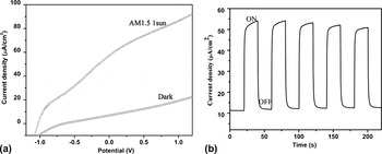
For potential application in energy generation, the twofold symmetric SnO2/TiO2 nanodendrite sample grown for 5 min was investigated for PEC water splitting. A three electrode system was adopted using 1 M NaOH solution as the electrolyte, platinum sheet as the counter electrode, and Ag/AgCl as the reference electrode. Figure 7(a) shows the linear sweep voltammagrams recorded in the dark and with illumination of AM1.5 1 sun. Upon illumination, the SnO2/TiO2 showed pronounced photocurrent starting at ∼−1.0 V and continues to increase to 85 μA/cm2 at +1.0 V. No saturation of photocurrent is observed even at more positive potential, which indicates efficient charge separation in SnO2/TiO2 upon illumination. The transient photocurrent curve [Fig. 7(b)] demonstrates the electrode has a fast photoresponse speed and reasonably good photostability. The relatively inferior performance of such SnO2/TiO2 dendritic nanostructured photoanode in comparison to previous reports on pure anatase TiO2 nanotubesReference Zhang, Hossain and Takahashi25 could be due to the higher contact resistances between TiO2 and SnO2 and between SnO2 and the Si substrate. Also, the overall spatial density of our dendritic nanostructure is still much lower than those highly packed TiO2 nanotubes by anodization. Nevertheless, there is much room for improvement by, e.g., growing such structures on more conductive substrate, increasing the overall spatial density of the dendritic nanostructures and increasing the electric conductivity of the SnO2 nanowire stem and surface sensitization by semiconducting nanoparticles of CdS.Reference Banerjee, Mohapatra, Das and Misra26, Reference Lin, Lu, Hsieh and Chien27
Photoelectrochemical performance of SnO2/TiO2 dendritic nanostructures as the photoanode. (a) Linear sweep voltammagrams collected in the dark and at AM1.5 (100 mW/cm2) illumination. (b) Amperometric I–t curves measured at an applied bias of +0.5 V at 100 mW/cm2 with 20 s light on/off cycles.

IV. CONCLUSION
In summary, a general solution heteroepitaxy growth method is used for the successful fabrication of quasi 2D SnO2/TiO2 dendritic nanoheterostructures. Electron microscopy characterizations reveal a perfect epitaxial relationship between the SnO2 nanowire trunks and TiO2 nanorod branches, which is the determining factor for the different growth direction,  , of the TiO2 nanorods from the usual [001]. When used as photoanode material, such hybrid nanowires might be useful for PEC water splitting applications, especially after further improvement strategies are adopted.
ACKNOWLEDGMENT
We thank Mr. G.Z. Sun and Prof. L.X. Zhen, in School of Mechanical and Aerospace Engineering, Nanyang Technological University, for providing the electrochemical workstation.