Introduction
Phased array radar has advantages including adaptability to various complex meteorological conditions, a long detection distance, and high resolution [Reference Yu, Hong, Jiang and Zhang1]. The advanced communication technologies which make the interconnection of everything feasible in the future is under active investigation [Reference Lin and Ziolkowski2]. However, in the research of traditional phased array antenna, there exist drawbacks such as narrow bandwidth [Reference Maximidis, Caratelli, Toso and Smolders3–Reference Yang, Ban, Li, Sun and Sim5], high cost [Reference Palmer, Yeary, Schvartzman, Salazar-Cerreno, Fulton, Bodine, Kirstetter, Sigmarsson, Yu, Zrnić, Meier and Herndon6], high profile [Reference Fofana, Fuchs, Avrillon, Colombel, Lézé and Palud7, Reference Baldazzi, Al-Rawi, Cicchetti, Smolders, Testa, van Coevorden Moreno and Caratelli8], and lack of generalizability. The adoption of the modular subarray design with broadband characteristics can improve these drawbacks.
The CP antenna has the merits of anti-attenuation, anti-multipath interference, and anti-multipath reflection [Reference Wei, Liao, Xue and Che9–Reference Bu and Qu11]. Therefore, it is widely applied in fields such as radar, navigation and satellite communications. There exist some basic types to achieve broadband CP antennas, such as microstrip slot antenna, substrate integrated waveguide slot antenna, loop antenna, monopole antenna, slot monopole antenna, and dipole antenna. In [Reference Mu, Zhao, Xiao, Niu, Fu and Zheng12], a dipole 8 × 8 CP phased array antenna with a stripline-to-slotline balun was discussed. The array antenna has a bandwidth of 2–12 GHz (142.8%) and ±60° scanning range. In [Reference Duan, Zhu, Wang and Geyi13], a CP heterogeneous antenna array is proposed. The array consists of one top element and six identical side elements. It has ±60° scanning range within the working bandwidth range of 3.2–3.8 GHz (17.1%). In [Reference Feng, Li, Cao, Liu, Yang and Wei14], a broadband CP cross-dipole antenna with a 3-dB AR bandwidth of 85.5% (1.94–4.84 GHz) was achieved. While these antennas exhibit excellent performance, they have relatively high-profile heights of 0.32λ, 0.55λ, and 0.38λ, respectively.
The microstrip patch antenna, valued for its low profile, cost-effective manufacturing, lightweight design, and well-defined radiation properties [Reference Wang, Zhao, Sun, Du, Yang and Yang15], has gained widespread adoption in millimeter-wave band antenna applications. In [Reference Yang, Zhou, Yu and Li16], a sequential phase feed 2 × 2 patch array was proposed. The antenna array achieves a 3-dB AR bandwidth of 4.52–5.4 GHz (17.7%). In [Reference Zhang, Hong, Ding, Yang, Zhu and Hu17], a 1 × 32 left-handed circular polarization (LHCP) phased array using 3 × 3 patch antenna elements was proposed. The AR bandwidth of 24.15–27.5 GHz (12.97%) and the scanning range of ±42° were achieved. In addition, compared with single-CP antennas [Reference Mu, Zhao, Xiao, Niu, Fu and Zheng12, Reference Duan, Zhu, Wang and Geyi13, Reference Yang, Zhou, Yu and Li16–Reference Kim, Chae, Jo, Yeo and Yu19], dual-CP antennas can reduce the antenna aperture size, enhance aperture utilization, and increase the capacity of the communication system. Many articles have studied dual-CP antennas. In [Reference Mao, Gao, Wang and Sri Sumantyo20], by composing different coupling elements in the two input paths, an intrinsic ±90° phase difference is obtained to realize dual-CP. The antenna has an AR bandwidth of 4.9–5.5 GHz (11.5%). In [Reference Yang and Rahmat-Samii21], dual-CP is achieved through reconfigurability enabled by PIN diodes. Dual-CP can also be achieved through dual orthogonal microstrip line feeding [Reference Saini and Dwari22, Reference Chandu and Karthikeyan23] or by designing a dual-CP feeding network [Reference Liu, Cheng and Yao24, Reference Wang and Qu25]. In [Reference Wang and Qu25], an aperiodic dual-CP scanning array based on the perturbation principle was proposed. The proposed aperiodic array has an AR bandwidth of 3–5.3 GHz (55.4%) and a scanning range of ±45°. In [Reference Li, Guo and Hao26], an aperture-coupled patch phased array is proposed, which provide dual-linear polarization (LP) and dual-CP. Its scanning range is ±50° and the AR bandwidth is 17.7–21.2 GHz (17.99%). To improve the bandwidth, a stacked microstrip patch can be used [Reference Yang, Zhou, Yu and Li27]. However, higher-order modes may emerge on the patches as the frequency increases. Some solutions have been proposed in [Reference Ding, Wu, Wen, Wu and Li28], where parasitic elements have been placed around the master radiating patch to improve both impedance bandwidth and gain flatness. Nevertheless, this comes at the expense of an increased antenna footprint.
In this paper, a low-profile dual-CP active phased array modular subarray is proposed. The subarray elements adopt stacked microstrip patch antennas, with adjacent resonant points introduced to effectively broaden the bandwidth. The dual-CP phase-shift network is designed with two input ports. By applying signals to different input ports, a ±90° phase difference can be generated at the output port. Combined with the transmitter/receiver (T/R) module, the proposed subarray can freely synthesize and switch between LHCP and right-handed circular polarization (RHCP). The feeding method employs the mirror-feed technique to counteract the impact of asymmetry, thereby improving the consistency of scanning gain and AR at both positive and negative angles. Meanwhile, employing Frequency Division Multiple Access (FDMA) technology, it can simultaneously form LHCP and RHCP beams for scanning. Finally, an 8 × 8 scale phased array composed of modular subarrays was fabricated and measured, with the simulated and measured results showing good agreement.
Analysis and design of the proposed modular subarray
Proposed antenna element structure
The proposed modular subarray element structure is shown in Fig. 1. The antenna element consists of a slave radiation layer, dielectric layer 1, an air layer, a master radiation layer, dielectric layer 2, metal layer 1, dielectric layer 3, a network layer, dielectric layer 4, and metal layer 2, arranged from top to bottom. Dielectric layer 1 is made of FR4 (εr = 4.4, tan δ = 0.02), while dielectric layers 2, 3, and 4 are composed of TSM-DS3 (εr = 3.0, tan δ = 0.0011)
Proposed antenna element with (a) 3D view, (b) perspective view.

The antenna element is a stacked microstrip patch antenna employing dual-feed points and electromagnetic coupling feed methods. It is composed of two parts: the antenna radiator and the dual-CP phase shift network. The antenna radiator part includes the slave radiation layer, dielectric layer 1, air layer, master radiation layer and dielectric layer 2. The master and slave radiation layer are rhombic patches with different side lengths, printed on the dielectric layer. Their side lengths are 6.9 and 5 mm, respectively. The master radiation antenna radiates LHCP and RHCP waves into space, while the slave radiation antenna broadens the bandwidth and enhances the gain.
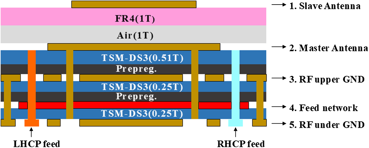
The dual-CP phase shift network part employs a stripline structure, consisting of metal layer 1, dielectric layer 3, phase shift network layer, dielectric layer 4 and metal layer 2. Metallized vias are designed in dielectric layer 2 and dielectric layer 3 to connect the phase shift network and the master radiation antenna. As shown in Fig. 1(b), by reasonably arranging metalized grounding holes, a cavity-like structure can be effectively formed to block the coupling crosstalk between each antenna element. Additionally, connecting the upper and lower metal layers of the stripline can effectively eliminate the resonance, which can effectively improve the active VSWR of the dual-CP phased array modular subarray.
In addition, Fig. 2 shows the profile of the proposed multilayer antenna element. The antenna element consists of five metal layers, each with a thickness of 1 ounce, four dielectric layers and one air layer. Among them, the thicknesses of dielectric layer 1, air layer, dielectric layer 2, dielectric layer 3 and dielectric layer 4 are 1, 1, 0.51, 0.254, and 0.254 mm, respectively.
Proposed antenna element with multilayer configuration.

The antenna element is driven by a miniaturized dual-CP feeding network, with each port responsible for generating either LHCP or RHCP. The introduction of the air layer and the use of the radiation patch effectively expand the bandwidth. Meanwhile, this low-profile design (with a profile height of 0.12λ) is highly conducive to vehicle conformability, which reduces the complexity of engineering applications.
Design of antenna element
The bandwidth of a single-layer microstrip patch antenna is relatively narrow. To enhance the bandwidth, a stacked microstrip patch configuration is employed. By adjusting the Interlayer dielectric thickness (h) and the patch dimensions (L1, L2), the resonance frequencies of the master and slave patches are brought closer together, resulting in a continuous wideband response. The resonant frequency is expressed as follows:
 \begin{equation}{f_n} = \frac{c}{{2\left( {{L_n} + \Delta L} \right)\sqrt {{\varepsilon _{r,{\text{eff}}}}} }},\end{equation}
 \begin{equation}\Delta L = 0.412h\frac{{({\varepsilon _{r,{\text{eff}}}} + 0.3)(W/h + 0.264)}}{{({\varepsilon _{r,{\text{eff}}}} - 0.258)(W/h + 0.8)}},\end{equation}
 \begin{equation}{\varepsilon _{r,{\text{eff}}}} = 0.5\left[ {{\varepsilon _r} + 1 + \left( {{\varepsilon _r} - 1} \right){{\left( {1 + \frac{{10h}}{W}} \right)}^{ - 0.5}}} \right],\end{equation}
where Ln is the length of the patch in the nth layer,  $\Delta L$is the edge extension correction, ɛr, eff is the effective dielectric constant, W is the patch width, and ɛr is the relative permittivity of the substrate.
The total bandwidth after stacking is given by the following relationship between the bandwidths of the primary and secondary patches:
 \begin{equation}{B_{{\text{total}}}} = \sqrt {B_1^2 + B_2^2 + 2k{B_1}{B_2}} ,\end{equation}
where B1 and B2 are the bandwidths of the master and slave patches, respectively. k is the interlayer coupling coefficient, which is dimensionless and represents the strength of electromagnetic coupling between the layers. It typically ranges from 0 (no coupling) to 1 (maximum coupling), with stronger coupling leading to a wider total bandwidth. Increasing the interlayer dielectric thickness h can reduce interlayer coupling k ( $k \propto 1/h$). During design, a balance must be struck between bandwidth and interlayer dielectric thickness.
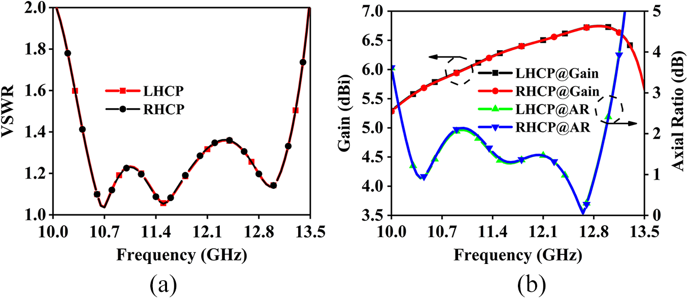
As shown in Fig. 3, the proposed antenna element attains optimized performance through careful tuning of the resonant frequencies of its master and slave patches, as well as the integrated phase-shift network. The VSWR of both LHCP and RHCP ports remains below 2 within the frequency range of 10.04–13.5 GHz (29.3%). The antenna element achieves a gain exceeding 5.3 dBi over 10.0–13.5 GHz (29.8%), while maintaining an axial ratio (AR) below 2.5 dB within 10.17–13.06 GHz (24.9%). Furthermore, it can be observed from the result diagram that the simulation results for both LHCP and RHCP are perfectly consistent, a result attributed to the complete symmetry of the antenna radiation layer and the 3-dB bridge network structure. This indicates that the antenna element has great potential for application in a wide range of scenarios.
Proposed antenna element with (a) VSWR and (b) gain and AR of LHCP and RHCP with frequency.

Design of phase-shift feed network
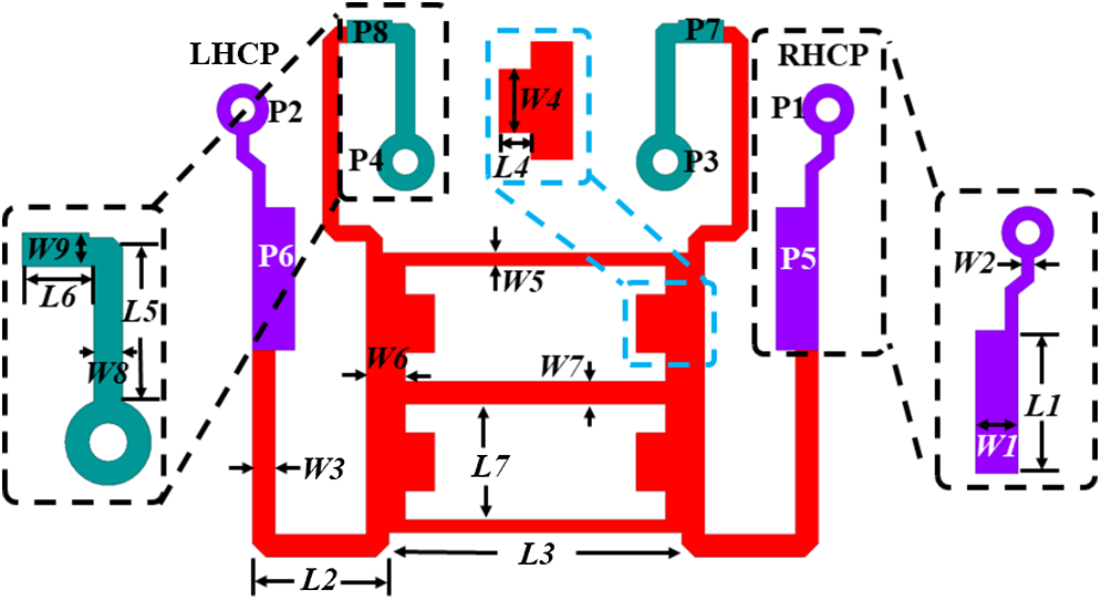
The miniaturized 3-dB bridge-type phase-shift network is shown in Fig. 4, and its size is shown in Table 1. The key to achieve dual-CP is that the miniaturized 3-dB bridge phase shift network provides the amplitude and phase required for CP. Port 1 and port 2 (labeled as P1 and P2 in Fig. 4) correspond to RHCP and LHCP feed ports in Fig. 2 respectively. Feed ports 1 and 2 provide a phase difference of 90° and −90° with respect to ports 3 and 4 (labeled as P3 and P4 in Fig. 4).
Proposed 3-dB bridge phase shift network.

Size of phase shift network

The two ports of each antenna element are independently connected to one radio frequency (RF) channel, which can independently control the amplitude and phase of the excitation. To achieve simultaneous dual-CP, FDMA technology is employed, allowing the antenna element to excite signals of different frequencies at port 1 and port 2 simultaneously.
Since the feeding network and radiation patch are inseparable components of the stacked microstrip antenna, impedance matching between them is crucial. Therefore, in this communication, an impedance matching method is employed to adjust the matching characteristics at the connector. By introducing high and low impedance lines at the positions labeled as P5, P6, P7, and P8 in Fig. 4, the matching performance at the connector ports is significantly enhanced.
The feeding network designed on this basis has excellent VSWR, amplitude and phase in the band. It can be seen from Fig. 5 that in the frequency range of 10.23–12.77 GHz (22.08%), the isolation is less than −13.2 dB, the VSWR of port 1 and port 2 are less than 1.71, the VSWR of port 3 and port 4 are less than 1.58, the amplitude difference is less than 0.35 dB, and the phase difference is less than ±4.1° in the frequency range of 10.23–13.8 GHz (22.08%).
Proposed 3-dB bridge phase shift network with (a) isolation, (b) VSWR, (c) insertion loss, and (d) phase.

Design and measurement of proposed subarray
In traditional phased array antenna design, varying scenarios necessitate different antenna sizes. While customizing antennas for specific applications can yield optimal performance, it also introduces design challenges, extended development cycles, higher cost, and increased complexity in both usage and maintenance.
To reduce the complexity of engineering applications and enhance versatility, a dual-CP modular subarray is constructed using the aforementioned dual-CP antenna elements, as shown in Fig. 6. The modular subarray consists of 64 dual-CP antenna elements. To address challenges such as the wiring of the feeding network, connector placement, and the avoidance of grating lobes during scanning, a spacing of 13 mm (0.49λ) is chosen as the optimal array configuration. Each subarray has a complete structure and function, allowing it to be used independently or extended as needed.
(a) Schematic diagram of the active phased subarray prototype. (b) Modular subarray design employs the mirror-feed technique.

It can be clearly seen in Fig. 6(b) that the structure of the pitch plane is completely symmetrical, which is conducive to ensuring the scanning consistency of the phased array antenna at the positive and negative angles of the pitch plane. Additionally, to counteract the effects of asymmetry in the azimuth plane, the mirror-feed technique facilitates the expansion of both gain and AR bandwidth.
The schematic diagram and prototype diagram of the T/R module are shown in Fig. 7(a) and Fig. 7(b). Each dual-CP antenna outputs two ports of LHCP and RHCP. Each RF channel contains low noise amplifier, power divider, switch, power amplifier, phase shifter, attenuator and equalizer. Each subarray is equipped with two combiners to simultaneously form two beams. By switching the switch, LHCP or RHCP can be selected as needed.
Transmitter and receiver module with (a) circuit diagram and (b) fabricated die photo.

The active VSWR simulation results of the modular subarray are shown in Fig. 8. The active VSWR remains below 2 for azimuthal LHCP, azimuthal RHCP, elevation LHCP, and elevation RHCP in the frequency ranges of 10.23–13.52 GHz (27.71%), 10.17–13.56 GHz (28.57%), 10.14–13.35 GHz (27.33%), and 10.15–13.38 GHz (27.45%), respectively.
Simulated active VSWR of azimuth plane of the subarray with (a) LHCP and (b) RHCP, elevation plane with (c) LHCP and (d) RHCP.

As shown in the AR simulation results of the modular subarray in Fig. 9, it is observed that the AR for azimuthal LHCP, azimuthal RHCP, elevation LHCP, and elevation RHCP remains below 3 dB within the frequency ranges of 10.2–13.15 GHz (25.27%), 10.2–13.15 GHz (25.27%), 10.05–12.77 GHz (23.84%), and 10.05–12.77 GHz (23.84%), respectively. For ± 60° beam scanning, the AR for azimuthal LHCP, azimuthal RHCP, elevation LHCP, and elevation RHCP remains below 6 dB within the frequency ranges of 10.18–13.34 GHz (26.87%), 10.18–13.34 GHz (26.87%), 10.2–12.8 GHz (22.61%), and 10.21–12.81 GHz (22.59%), respectively.
Simulated AR of azimuth plane of the subarray with (a) LHCP and (b) RHCP, elevation plane with (c) LHCP and (d) RHCP.

By considering all polarization states and scanning directions, the overall frequency range in which the active VSWR remains below 2 and the AR stays below 3 dB (±45°) and 6 dB (±60°) is determined as the common range among these cases. This range is 10.23–12.77 GHz (22.08%).
The proposed subarray prototype along with the near field and far field test environments are shown in Fig. 10. Since the structures and results of LHCP and RHCP are essentially identical, the LHCP data are omitted in this paper, and only the RHCP results are presented.
Prototype of the active phased subarray with (a) beam control and power supply, (b) fabricated prototype and the measurement in the anechoic chamber, (c) antenna array surface, and (d) far-field measured environment.

The simulated and measured radiation patterns and AR results are shown in Fig. 11, where only the gain and AR in the main beam region for each scanning angle are displayed for clarity. The corresponding quantitative results at representative frequencies are summarized in Table 2.
Measured and Simulated gain and AR for the azimuth and elevation plane of the subarray at (a) 11.45 GHz of azimuth plane, (b) 12.10 GHz of azimuth plane, (c) 12.75 GHz of azimuth plane, (d) 11.45 GHz of elevation plane, (e) 12.10 GHz of elevation plane, and (f) 12.75 GHz of elevation plane.

Comparison of simulation and measurement results

The results show good agreement between the simulated and measured radiation patterns. Slight differences are observed between the measured and simulated peak gains at 11.45, 12.1, and 12.75 GHz, while the gain drop trends during scanning remain consistent. Similarly, while the measured AR results are generally slightly worse than the simulation, a small portion of the measured AR values are comparable to or even better than the simulated results. Overall, the trend between simulation and measurement remains consistent.
To highlight the novelty of the proposed design, a comparative study of some other competitive phased array antennas is shown in Table 3. Compared with the reported works, the proposed array achieves a wider AR bandwidth, a lower profile, and a larger 2D scanning range under dual-CP operation. These results confirm the superior performance of the proposed design in terms of polarization diversity, bandwidth, and structural compactness.
Comparison between reported works and proposed antenna

Conclusion
In this paper, a novel wideband low-profile dual-CP active phased array modular subarray is designed, analyzed, and measured. The proposed subarray is based on the wideband dual-CP antenna element to achieve radiation, with beam synthesis and switching performed by the T/R module. The mirror-feed technique is employed to improve the consistency of scanning beams at both positive and negative angles. Additionally, the modular design enables the construction of active phased array antennas of various sizes, allowing adaptability to different application scenarios. Finally, an array prototype is fabricated to verify its scanning capability of ±60° in both the azimuth and elevation planes. With the advantages of low profile, a wide bandwidth (22.08%) and a broad scanning angle, the proposed subarray is suitable for various application scenarios that require beam scanning.
Acknowledgement
This work is supported in part by the Scientific Research Program Funded by the Shaanxi Provincial Education Department (No. 22JC058), the Technology Innovation Leading Program of Shaanxi (No. 2024ZC-YYDP-33), and the Interdisciplinary Research Program of the School of Electronic Engineering, Xi’an University of Posts and Telecommunications (No. XKJC2507).
Competing interests
The author(s) declare none

Yunqi Zhang received the B.E., M.E., and Ph.D. degrees from Xidian University, Xi’an, China, in 2009, 2012, and 2015, respectively. He is currently with Xi’an University of Posts and Telecommunications. His research interests include circularly polarized antennas, orbital angular momentum (OAM), and phased array antennas.

Quanbo Liu received the B.S. degree in Electromagnetic Fields and Wireless Technology from Xianyang Normal University (XYNU) in 2023. He is currently pursuing the M.S. degree in the School of Electronic Engineering, Xi’an University of Posts and Telecommunications (XUPT), where his research focuses on sparse arrays

Xinwei Wang received the B.S. degree in Electronic Science and Technology from Weifang University, China, in July 2011, and the M.S. degree in Electronics and Communication Engineering from Xi’an University of Posts and Telecommunications (XUPT), China, in July 2014. He is currently pursuing the Ph.D. degree at XUPT, and his research interests focus on BeiDou Satellite Navigation System (BDS) technologies.

Shanzhe Wang (M’22) received the M.S. and Ph.D. degrees in Electronic Science and Technology from Beijing Jiaotong University, Beijing, China, in 2017 and 2022, respectively. In 2022, he joined the School of Electronic Engineering, Xi’an University of Posts and Telecommunications, as a Lecturer. His current research interests include beam-scanning antennas and leaky-wave antennas.

Zhian Wang is currently pursuing the B.S. degree in Electromagnetic Fields and Wireless Technology at the School of Electronic Engineering, Xi’an University of Posts and Telecommunications (XUPT), China.

Wenjia Zhou received the Ph.D. degree in Engineering from Northwestern Polytechnical University (NPU) in 2017. In the same year, she joined the Department of Electronic Information, School of Electronic Engineering, Xi’an University of Posts and Telecommunications (XUPT). Her recent research and teaching interests include antenna theory and engineering, satellite navigation and communication, radar signal delay analysis, and simulation techniques.

Jiateng Chen received the B.S. degree from Xi’an University of Posts and Telecommunications (XUPT) in 2019, and the M.S. degree from the School of Electronic Engineering, Xi’an University of Posts and Telecommunications (XUPT), in 2024. His research focused on phased array antennas.