Introduction
As one of the most important components in dye-sensitized solar cells (DSSCs), the noble metal platinum is often used as counter electrode because of its superior electrocatalytic activity, high electrical conductivity as well as good chemical stability.[Reference O'Regan and Gratzel1] In view of the limited reserve and high cost of Pt, it is highly important to search for less expensive Pt-free counter electrode alternatives with a similarly high electrocatalytic activity for future development of DSSCs. In recent years, various low-cost alternatives to platinum in DSSCs have been investigated,[Reference Wu, Lin, Wang, Wang, Guo, Qi, Peng, Hagfeldt, Grätzel and Ma2] including carbon materials,[Reference Jiang, Li, Wang and Gao3, Reference Kavan, Yum and Gratzel4] conducting polymers,[Reference Saito, Kitamura, Wada and Yanagida5, Reference Wu, Li, Fan, Lan, Li, Lin and Hao6] transition metal nitrides,[Reference Jiang, Li and Gao7, Reference Li, Song, Pan and Gao8] sulfides,[Reference Wang, Anghel, Marsan, Ha, Pootrakulchote, Zakeeruddin and Gratzel9, Reference Sun, Qin, Huang, Guo, Li, Luo and Meng10] carbides,[Reference Wu, Lin, Hagfeldt and Ma11] oxides[Reference Wu, Lin, Hagfeldtb and Ma12, Reference Lin, Wu, Wang, Hagfeldt and Ma13] and most recently phosphide.[Reference Dou, Li, Song, Pan and Gao14] But seldom included in all these materials, except for carbon materials, are one-dimensional (1D) nanostructures. In principle, the electrocatalytic activity of Pt-alternative materials is not only related to their intrinsic electronic structure but also related to their structure and morphology. Typically, a highly efficient counter electrode of DSSC needs to have a large surface area, high electrical conductivity and an open structure for accommodating and rapidly transporting electrolyte of iodide/tri-iodide.[Reference Jiang, Li and Gao7] Usually, a large surface area comes with more grain boundaries between the nanoparticles, a feature that can hinder electron transport. In this sense, 1D nanomaterials such as nanowires and nanotubes are advantageous due to the possibility of having both high electrical conductivity and superior electrocatalytic activity. The porous Ni2P nanowires reported here represent a glaring example of such 1D nanomaterials.
Transition metal phosphides are known to have noble metal-like catalytic activity, good electrical conductivity and high chemical stability. The purpose of this work was to develop a new strategy to synthesize 1D nanomaterial of Ni2P and explore its use as DSSC counter electrode. To this end, we first synthesized self-assembled Ni(SO4)0.3(OH)1.4 nanobelts precursor by the hydrothermal method. Then through phosphatization of the Ni(SO4)0.3(OH)1.4 nanobelts precursor, we have created a new kind of porous Ni2P nanowires. Significantly, such porous Ni2P nanowires have demonstrated the excellent electrocatalytic characteristics when used as a replacement of Pt for the counter electrode of DSSCs.
Experimental results
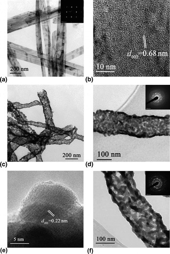
The self-assembled Ni(SO4)0.3(OH)1.4 nanobelts look very thin and uniform (see Fig. 1 and Fig. S1 in Supplementary materials), which measure 100–200 nm in width. Actually, these belts are composed of even smaller single nanobelts. For a single nanobelt, the thickness is about 4–6 nm and the width is about 50 nm. Most of the single nanobelts are paralleled and layered together forming the bigger, 100–200 nm wide nanobelts. The selected area electron diffraction (SAED) pattern [Fig. 1(a)] clearly shows the single-crystalline pattern of the nanobelts. As shown in the scanning electron microscopy (SEM) and transmission electron microscopy (TEM) images, the nanobelts of Ni(S04)0.3(OH)1.4 turned to the as-formed porous Ni2P nanowires after the phosphatization in the toluene solution containing yellow phosphor at the temperature of 200 °C. The middle of the wires looks hollow and porous, and the diameter of the most wires is about 100–250 nm. The TEM images in Fig. 1 clearly illustrating the porous nanowires are made of closely connected nano grains, the most grains diameter of the wires is about 10–25 nm. And the nanowires are porous with a lot of nano holes spread in the grains, which also means a large surface area. The high-resolution transmission electron microscopy (HR-TEM) image in Figs. 1(b) and 1(e), together with the SAED pattern in Figs. 1(a) and 1(d), identifies the lattice spacing of 0.68 nm can be ascribed to the (0,0,2) planes of monoclinic Ni(SO4)0.3(OH)1.4, and the lattice spacing of 0.22 nm can be ascribed to the planes (2, 0, 1) of hexagonal Ni2P (see Refs. S1 and S2). All the HR-TEM images and the SAED patterns in Fig. 1 are consistent with the parameters of the X-ray diffraction (XRD) patterns shown in Fig. S3. So together with the XRD, SEM and the TEM, it is reasonable to conclude that the porous Ni2P nanowires are formed because of the lattice shrinkage of Ni(SO4)0.3(OH)1.4 precursor nanobelts induced by chemical transformation. Specifically, after the phosphatization, the lattice shrank leading to the structural reconstruction, namely, the 1D physical twisting/merging to porous wires. The Ni2P nanowires could keep the nanowire morphology after it was sintered for 1 h at 400 °C in the Ar atmosphere [as shown in Fig. 1(f) and Fig. S2(d)]. On the other hand, the SAED pattern and the XRD pattern [Fig. S3(b)] show that the hexagonal phase is maintained, although the grains are somewhat larger. And there are still many perhaps even larger nanoholes spread on the nanowires, and the grains are still closely connected together.
TEM images of Ni(SO4)0.3(OH)1.4 nanobelts (a, b), Ni2P nanowires (c–e), Ni2P nanowires 400 °C (sintered in Ar atmosphere) (f).

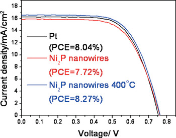
Figure 2 shows the J–V characteristic curves of the DSSCs with Pt, Ni2P nanowires and Ni2P nanowires 400 °C (sintered in Ar atmosphere) as counter electrodes. The detailed photovoltaic parameters from the J–V curves and the electrochemical impedance spectra are summarized in Table I. In general, the Ni2P nanowires electrode presents an excellent photovoltaic performance, comparable with the Pt counter electrodes.
J–V characteristic curves of DSSCs with different counter electrodes of the Pt, as-formed Ni2P nanowires and Ni2P nanowires 400 °C (sintered in Ar atmosphere), measured under simulated sunlight of 100 mW/cm2 (AM 1.5).

Photovoltaic parameters of DSSCs with different counter electrodes.

As the counter electrodes of DSSCs, the surface electrocatalytic activity is an important factor for the photovoltaic performance. Not only the superb intrinsic property of Ni2P, but also the trifunctional structure of large surface area, high electrical conductivity and convenient structure for the iodide/tri-iodide transportation, are of benefit to the high electrocatalytic activity. The self-assembled Ni2P nanowires just fulfill these requirements, qualifying it as a high-performance counter electrode materials for DSSCs. The large surface area resulting in a little charge-transfer resistance between the electrolyte/electrode interface. The closely connected grains of the wires resulting in an efficient electron transport network and high electrical conductivity for the electron transportation. The porous structure of the electrode made of nanowires providing convenient pathway for the iodide/tri-iodide transportation. Therefore, such a trifunctional structure is more preferable not only for little charge-transfer resistance, convenient electron transportation path and good electrical conductivity, but also for the convenient transportation of iodide/tri-iodide in the electrolyte, contributing to the enhanced photovoltaic performance. What is more, the source of the Ni2P material is abundant as compared with the noble metal Pt, and the chemical stability of Ni2P in contact with the electrolyte can be directly translated into the good stability of DSSCs which use the 1D porous Ni2P nanowires counter electrode (see Fig. S6).
Conclusions
In summary, we have for the first time succeeded in synthesizing 1D porous Ni2P nanowires through the easy phosphatization of a nanobelt precursor. The novel porous nanowires have been first investigated as highly efficient and low-cost counter electrodes of DSSCs. The phosphatization of the Ni(SO4)0.3(OH)1.4 nanobelts led to the formation of the porous Ni2P nanowires, which were driven by the built-in strain and thereby self-assembled into the porous Ni2P nanowires via a twisting/merging mechanism in an easy way. This nanostructure enjoys a large surface area, amenability to form a closely connected electron transport network imparting convenient transport of both electrons and the iodide/tri-iodide electrolyte and the high superior electrocatalytic activity. Our findings have general implications in the fabrication of porous functional nanowires through the chemical transformation and the subsequent strain-induced physical twisting/turning mechanism from nanobelt precursors. Indeed, the excellent DSSC performance has been achieved when the porous Ni2P nanowires were used as counter electrode, which is comparable to that of the conventional Pt counter electrode. Clearly, the porous Ni2P nanowires have great potential as a low-cost alternative to the expensive noble metal Pt in the future developments and applications of DSSCs.
Acknowledgments
This work was supported by the HK-RGC General Research Funds (GRF Nos. HKUST 604809 and 605710) and HKUST (SRFI11EG17-D).
Supplementary materials
For supplementary material for this article, please visit http://dx.doi.org/10.1557/mrc.2012.16