I. INTRODUCTION
Orthogonal frequency-division multiplexing (OFDM) modulation schemes enable robust signal transmission in severe multi-path fading environments. High spectral efficiency can be reached but the large peak to average power ratio (PAPR) of OFDM signals results in a difficult challenge for power amplifier (PA) design to meet both linearity and power efficiency performances.
Linearity requirements can be met at significant output power back-off to the detriment of power added efficiency (PAE). Meeting linearity requirements like error vector magnitude (EVM) or ACPR at high PAE can be achieved if one implements a dynamic supply voltage in accordance with input envelope power variations. The leading idea is to maintain a quasi-constant saturated gain of PAs [Reference Nam and Kim1–Reference Deng, Gudem, Larson, Kimball and Asbeck7]. This challenge in PA design is of great interest when applied to high power (a few tens of watts or more). Nevertheless, in such conditions, the task is quite difficult because the dynamic supply voltage circuit must handle large DC current and voltage and a sufficiently wide bandwidth for an efficient processing of the base-band envelope signal.
In [Reference Bacqué8], experimental results obtained with a built-in 100 W LDMOS envelope tracking (ET) PA operating in a 50–500 MHz bandwidth and including base-band digital predistortion have been reported. This paper complements previous work reported in [Reference Bacqué8], by focusing on main steps and design rules to optimize the ET amplifier efficiency and linearity. A main aspect of this paper is to describe a straightforward methodology that has not been reported to our knowledge in this way in other similar works.
Section II of the paper focuses on the procedure followed for the extraction of drain bias control laws from multi-bias quasi-static AM/AM and AM/PM characteristics of the RF PA. The bias control circuit is then described and characterized under continuous-wave (CW) power swept excitations to validate its capability to be applied to high PAPR modulated signals with appropriate voltage range and high DC current when it is terminated into a low load impedance (in the order of a few ohms).
In Section III, the combination of ET technique and digital base-band predistortion [Reference Guo and Cavallaro9, Reference Besbes and Le-Ngoc10] is presented for an OFDM modulation scheme. It provides significant enhancements in PA linearity. The calibrated time domain envelope measurement system developed for this purpose is described. Key features concerning envelope time alignments are mentioned along with the predistortion algorithm implemented to take into account and compensate a part of the ET amplifier memory effects. Finally, we point out promising capabilities of the proposed technique and mention possible future trends to investigate.
II. DYNAMIC ET AMPLIFIER DESIGN
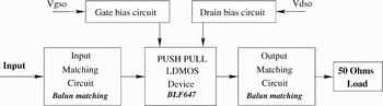
The wide-band high-PA used in this work is presented in Fig. 1. It is developed around a high-power LDMOS push–pull transistor (BLF647). The wide-band matching is done by using conventional semi-rigid coaxial baluns used at VHF/UHF frequencies [Reference Park, Burger and Titizian11]. The bias circuits are designed taking into account the amplifier stability and time-varying bias voltage requirements (voltage range, current handling, and frequency bandwidth).
Wide-band push–pull amplifier scheme.

A) Determination of the bias control laws
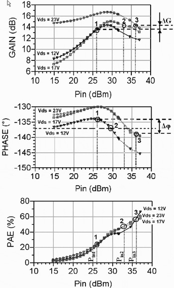
The development of an efficient bias control needs the determination of bias laws, which permits maintaining a constant complex gain in the compression zone. In a first step, AM/AM and AM/PM measurements enable the determination of the drain bias control function versus input power for the whole dynamic range that will be required for the OFDM signal used. An experimental test set-up, based on a vector network analyzer, was used to measure AM/AM and AM/PM characteristics with a CW stimulus. A nominal gain (14 dB/−137°) was chosen as shown in Fig. 2. In our case, the input power varies from 26 to 37 dBm. It corresponds here to a power range compliant with the OFDM signal having 11 dB PAPR. For different power levels in this range, the Vdso bias voltage is experimentally tuned until the nominal gain is approximately obtained. Figure 2 shows AM/AM and AM/PM characteristics obtained after Vdso adjustments for three different power levels.
Conversion characteristics and PAE measurements for selected bias conditions (Vgso = 5 V).

First, the reason to target this nominal gain is that it corresponds to the maximum PAE of the amplifier at about 2 dB gain compression and 28 V drain bias.
Second, it is important to mention here that the constant complex gain that is targeted and represented by a horizontal dotted line in Fig. 2 must be carefully checked and does not cross AM/AM and AM/PM curves at angular points or close to angular points. Otherwise, when continuous envelope variations and corresponding drain bias conditions are applied, severe ripples can arise in the complex gain profile of the ET amplifier. This will result in linearity performance degradation as well as increased difficulties expected for the base-band predistortion procedure and algorithm.
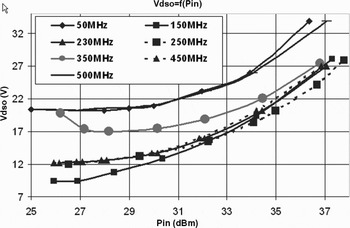
Third, class B operation has been chosen and a constant 5 V gate source bias voltage Vgso has been found to be relevant. In class B bias operation, the DC drain current of the amplifier is naturally controlled according to the RF input power level. This very interesting particularity of class B avoids the need to dynamically control the gate bias voltage. Bias laws (Fig. 3) are determined over the entire power range of the input signal and for a set of discrete frequencies. Figure 3 shows the optimal drain bias voltage Vdso necessary to maintain a constant 2 dB gain compression versus input power level. A 250 MHz CW carrier frequency has been chosen in Section III of this paper to validate the design methodology. At this carrier frequency, a 11–28 V voltage range is required for 10 dB input power variation that corresponds to the PAPR of OFDM signals.
Bias laws over the operating bandwidth versus input power Pin.

Finally, it is also verified that the ratio between drain bias voltage Vdso and DC drain current Idso remains almost constant at each point of the drain bias curve versus input power for a given carrier frequency. This ratio (Vdso/Idso) that is here, in our case, in the order of 4 Ω represents the resistive load impedance of the drain bias control circuits. All the design criteria mentioned above are important to ensure that the whole ET PA reaches good performances in terms of both PAE and linearity.
B) Dynamic bias hardware
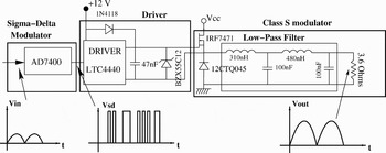
The available power, efficiency, and frequency bandwidth are three major features to be taken into account when designing the dynamic bias hardware. A maximum bias power is reached at the highest bias point of the RF amplifier (a 7 A drain current with a 28 V drain voltage in our case). Bias control circuits must exhibit the highest possible efficiency in order to keep the efficiency improvement of the overall system still interesting. Figure 4 shows the block diagram of the proposed system. The base-band envelope of the modulated signal is converted into a two-state switching signal using a ΣΔ modulator [Reference Keyzer, Hinrichs, Metzger, Iwamoto, Galton and Asbeck12, Reference Wang13, Reference Saari, Juurkko and Halonen14]. A class S modulator (or buck DC–DC converter), based on a fast-switching LDMOS transistor, feeds the drain bias port of the amplifier. The sampling frequency rate, regarding our application, should be at least 10 times the maximum frequency of the base-band signal.
ET PA.

Figure 5 shows the circuit developed with an AD7400 ΣΔ modulator running at 10 MHz maximum clock frequency. A high-speed switching MOSFET (IRF7471) is used and a Schottky diode (12CTQ045) is connected between the MOSFET source transistor and the ground plane. Due to the floating point on the source of the MOSFET, the use of a high-speed gate driver (LTC4440) is necessary. Furthermore, a 47 nF bootstrap capacitor is used to reduce the transition times. The low-pass output filter has a cut-off frequency of 1 MHz.
ΣΔ and class S modulator.

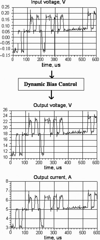
The measured efficiency of the drain bias circuit (ΣΔ+class S modulators) is about 90% for a 100 kHz input signal and a 10 MHz sampling frequency. Validation of this circuit was performed on a 3.6 Ω resistive load representative of the resistance of the drain DC access of the RF amplifier. A non-filtered 16QAM envelope waveform was used as an input signal for this test (see Fig. 6). A voltage range from 11 to 24 V was tuned. In accordance with the curve recorded at 250 MHz in Fig. 3, the ET circuit can be used for a modulated signal having 10 dB PAPR. This is the case of the OFDM signal used subsequently in this paper for the validation of the proposed technique. Measured output voltage and current are presented in Fig. 6; the measured peak power is about 150 W.
Drain bias control validation with a 3.6 Ω resistive load. Peak power = 150 W, bandwidth = 1 MHz, efficiency = 90% at 100 kHz.

III. COMBINED DIGITAL PREDISTORTION AND DRAIN DYNAMIC SUPPLY VOLTAGE TECHNIQUE
A) Test bench description
As mentioned in Section IIA, the ET PA may exhibit small complex gain ripple versus input envelope power variations. Although maximum attention has been paid to target a maximally flat complex gain trajectory, residual nonlinearities of the ET amplifier exist and can be efficiently compensated by base-band digital predistortion. The smoother the residual nonlinearities, the more efficient and simple the base-band predistortion method and algorithm. The research of a maximally flat complex gain in the design strategy reported here has motivated and justified the successive steps, starting from multi-bias static AM/AM and AM/PM characterization of the PA, tuning of the bias control circuit for appropriate voltage and current ranges, and then applying in a last step a base-band predistortion on the whole ET PA driven by an OFDM modulation scheme.
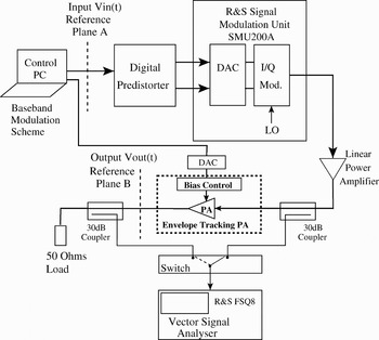
For base-band predistortion implementation, a test bench using a computer-controlled signal modulation unit and a vector signal analyzer was used as depicted in Fig. 7.
Test bench.

The dynamic range of the set-up is in the order of 60 dB. The OFDM modulation scheme is generated via a PC in the input reference plane A in Fig. 7 (base-band input signal Vin(t)). Complex envelope waveforms are measured with a vector signal analyzer and are error corrected using S parameters of cables, switches, and couplers. The complex output envelope waveform Vout(t) is measured in the output reference plane B in Fig. 7.
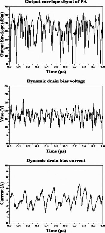
The time domain shapes of base-band signals used for digital predistortion and the ET bias system are obviously synchronized. Furthermore, they need to be properly time aligned or slightly delayed to reach maximum PA performances in terms of PAE and linearity. As an illustrative example, the time domain shapes of envelope signals at PA output and time-varying drain voltage and current are shown in Fig. 8. At 1 Mbit/s bit rate, the time delay between the PA input envelope and the bias command is not significant.
Base-band signal waveforms (predistortion is not applied here).

B) Digital base-band predistortion methodology
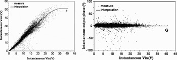
A first step consists in the measurement of the envelope transfer function between input and output reference planes A and B (see Fig. 7). Digital predistortion is not applied in this first training step and the characterization approach consists in the extraction of dynamic AM/AM and AM/PM characteristics from instantaneous input/output complex envelope waveform measurements. Preliminary to dynamic AM/AM and AM/PM characteristics extraction, input and output envelope waveforms must be time aligned. For that purpose, a cross correlation function between input and output waveforms is computed. An average time delay is then determined and compensated to obtain time-aligned input and output envelope waveforms [Reference Nanfack Nkondem15]. Dynamic AM/AM and AM/PM measurements are shown in Fig. 9. Measurements data spreading indicates the presence of memory effects.
Dynamic AM/AM and AM/PM conversions and fifth-order odd polynomial fit.

The average AM/AM characteristic, called F and plotted in continuous line in Fig. 9, is extracted by using the least mean square algorithm while the average AM/PM characteristic, called G, is extracted by using the Savitzky–Golay technique [Reference Savitzky and Golay16]. Inverse functions, respectively, denoted as F −1 and G −1, are then determined using the spline curve fitting technique and applied to input base-band modulated waveforms to achieve digital predistortion. In fact, F −1 acts as a gain multiplication factor normalized to the small-signal linear gain while G −1 acts as a phase compensation as illustrated in the block diagram in Fig. 10.
Digital predistorter.

C) Measurement results
The measurement conditions are summarized below:
• modulation scheme = OFDM,
• carrier number = 100,
• PAPR = 10.52 dB,
• RF frequency = 230 MHz,
• bit rate = 1 Mbit/s (250 kSymb/s)
• average output power = 44 dBm.
1) MEASURED OUTPUT SPECTRUM IN THREE DIFFERENT OPERATING CONDITIONS
Table 1 summarizes PAE and ACPR measurements at different operating conditions of the PA. Without digital predistortion, a 45 dBm output power is delivered with 38% PAE and 27 dB ACPR. This ACPR value was obtained at fixed drain bias and 8 dB input power back-off. The dynamic supply voltage technique enables a PAE improvement of 10 points as compared with the back-off technique. Furthermore, the linearity is enhanced. The bias command combined with digital predistortion improves the efficiency and linearity even if significant memory effects exist in the PA. When digital predistortion is applied to the ET-PA, one point of PAE is lost but an improvement of 5 dB ACPR is obtained.
Measured performances in different operating conditions.

Figure 11 shows the output spectrum at three operating conditions. The drain bias control associated with digital predistortion enables an ACPR improvement in the order of 15 dB, compared with fixed bias operation, and maximum PAE is maintained.
Output spectrum in three operating conditions (fixed bias, bias control, bias control and digital predistortion).

2) MEASURED PERFORMANCES OVER THE FREQUENCY BANDWIDTH OF THE AMPLIFIER
The control bias system was tested at various center carrier frequencies over the PA frequency bandwidth. Figures 12 and 13 show that both efficiency and ACPR are improved independently of the RF frequency carrier.
PAE versus carrier frequency (bit rate = 1 Mbit/s, no digital predistortion applied).

ACPR versus carrier frequency (bit rate = 1 Mbits/s, no digital predistortion applied).

IV. CONCLUSION
An ET 100 W LDMOS PA has been presented along with a time domain envelope characterization test bench including digital base-band predistortion methodology. An important feature reported here is that the overall system is able to take into account a significant part of memory effects and to control base-band signal timing in order to reach the best PAE/ACPR trade-off. In all, 37% PAE and −32 dBc ACPR optimum performances have been reached at 230 MHz carrier frequency and 1 Mbit/s bit rate.
This paper has described a straightforward methodology to design a high-efficiency and linear ET amplification solution. This work was done for wireless military communication applications. The next generation of base station PAs for multiband and multi-standard communications can also be addressed. For wider envelope bandwidth applications, the switched DC supplies operation mode can be investigated and the use of GaN devices can also be of great interest.
 Ludovic Bacque was born in Perigueux, France, on September 7, 1980. He received a Ph.D. degree in communication engineering from the University of Limoges, France, in 2008. In 2008, he joined Prâna in Brive France as an engineer. His main research interests are design and optimization of high power microwave power amplifiers.
 Gregoire Nanfack-Nkondem received a B.S. degree in electrical engineering from Dschang University, Dschang, Cameroon, in 1999 and an M.S. degree in electrical engineering from the Limoges University, Faculty of Sciences and Technologie Limoges, France, in 2005. He received a Ph.D. degree in electrical engineering from the University of Limoges in 2008. His doctoral research concerns the enhancement of high-efficiency power amplifiers linearity for WLAN OFDM systems.
 Philippe Bouysse was born in Aurillac, France, in 1965. He received a Ph.D. degree in communication engineering from the University of Limoges, France, in 1992. From 1992, he has been with the University of Limoges, Brive, as a teacher and researcher with XLIM Laboratory. His main research interests are the modeling of microwave transistors and the design and optimization of microwave power amplifiers.
 Guillaume Neveux was born in Civray, France, in 1976. He received a Diplôme d'Etudes Approfondies (DEA) degree from the Universite Paris 11, Orsay, France, in 2000 and a Ph.D. degree in electronics and communications from the Ecole Nationale Superieure des Telecommunications (ENST), Paris, France, in 2003. From 2004, he has been with the Instrumentation Group, XLIM Laboratory, University of Limoges, France. His research interests include nonlinear measurements with a large-signal network analyzer (LSNA), the study of RF sampling systems, and homodyne demodulation of multimode and multiband RF signal for mobile applications with five-port technology.
 Jean Michel Nebus was born in 1963. He received a Ph.D. degree in electronics at the University of Limoges, France, in 1988. In 1988, he joined Alcatel Space Industries in Toulouse, France, as a system engineer for a telecommunication satellite payload. From 1990, he is a teacher–researcher at the university of Limoges (Xlim Laboratory), France. His main areas of research are large signal characterization of microwave power transistors and high-efficiency power amplifier design.
 William Rebernak received a Dipl-Ing degree from electrical higher school in Paris in 1973. From 1973 to 1983, he worked in the radio-diffusion and television division of Thomson CSF. He was in charge of FM, television, and CERN equipment development. From 1984 to 1991, he was responsible for emitter and power radio-diffusion antennas development. From 1992 to 1994, he was in charge of electromagnetic study teams in Thales Communications. Until 1995, he was responsible for upstream studies in Thales communications division. He also participated in several European programs such as ACTS, BIOMED, ESPRIT, PCRD, FIRST, PROMURA, SUCOM, SUAW, and VICTORIA.
 Luc Lapierre was born in Clermont-Ferrand, France, in 1957. He received a Dipl-Ing degree from Ecole Superieure d'Electricite (ESE) in Paris, Gif sur Yvette, in 1980. In December 1981, he joined the French National Space Centre (CNES) in Toulouse, where he was involved in microwave research activities mainly oriented on solid-state components. He also worked as technical support in the development of microwave equipments for satellite payloads. He has been the Head of CNES Microwave Department and now he is a Microwave Expert in the Microwave and Time Frequency Department.
 Denis Barataud was born in Saint-Junien, France, in 1970. He graduated from “Ecole Nationale Superieure de Telecommunications de Bretagne” in 1994. He received a Ph.D. degree in electronics from the University of Limoges, in 1998. He was a postdoctoral scientist for Microwave Laboratory of the CNES of Toulouse, France, from 1998 to 1999. From 2000, he has been with the XLIM (formerly IRCOM) Laboratory at the University of Limoges, where he became an assistant professor in 2001. His research interests include the development of time-domain equipment and techniques for the characterization of nonlinear devices.
 Raymond Quéré (senior member IEEE) received an electrical engineering degree from ENSEEIHT Toulouse, France, in 1976, the French aggregation in applied physics in 1978, and a Ph.D. degree from the University of Limoges in 1989. In 1992, he was appointed full professor at the University of Limoges, where he leads the nonlinear high-frequency devices, circuits, and systems research group at IRCOM-CNRS Laboratory. His main field of interest is in the area of nonlinear device and circuit modeling with particular emphasis on nonlinear phenomena such as stability in power amplifiers. He is involved in a number of technical program committees and serves as a reviewer for several journals such as Electronic Letters, IEEE Transactions on MTT, etc. In 2005, he was appointed as the general Chairman of the European Microwave Week in Paris.