I. INTRODUCTION
Scandium nitride (ScN) belongs to the family of transition metal nitrides and inherits its outstanding physical properties, including high mechanical hardness, thermal, and chemical stability. Reference Gschneider, Melson, Melson, Youngblood and Schock1–Reference Gall, Petrov, Hellgren, Hultman, Sundgren and Greene4 ScN—an indirect n-type semiconductor—has a band gap of 0.9 eV. Reference Saha, Acharya, Sands and Waghmare5 The values of the direct band gap lie in the range of 2.1–2.6 eV. Reference Moram, Barber and Humphreys6,Reference Dismukes, Yim and Ban7 An average electron mobility of about 100 cm2 V−1 s−1 has been reported for high quality sputtered ScN thin films. Reference Dismukes, Yim and Ban7–Reference Burmistrova, Maassen, Favaloro, Saha, Salamat, Koh, Lundstrom, Shakouri and Sands10 The electron concentration is usually in the degenerate range (1020–1022 cm−3) due to unintentional doping with oxygen during ScN thin film deposition. Reference Gregoire, Kirby, Scopelianos, Lee and van Dover8–Reference Kerdsongpanya, van Nong, Pryds, Zukauskaite, Jensen, Birch, Lu, Hultman, Wingqvist and Eklund11 Even under high vacuum conditions, oxygen incorporation occurs due to the high affinity of Sc for oxygen. Reference Gregoire, Kirby, Scopelianos, Lee and van Dover8–Reference Moram, Novikov, Kent, Nörenberg, Foxon and Humphreys12 It has been shown that the carrier concentration can be slightly reduced for ScN thin films obtained by gas source molecular beam epitaxy (GSMBE) with a base pressure of 10−10 Torr Reference King, Davis and Nemanich13,Reference King, Nemanich and Davis14 or by efficiently suppressing impurity concentration during hybrid vapor phase epitaxy (HVPE) using a home-designed corrosive-free HVPE reactor. Reference Oshima, Villora and Shimamura15 Oxygen, which forms a solid solution alloy with ScN, causes a shift of the Fermi energy into the conduction band without changing the density of states (DOS) of pure ScN, Reference Burmistrova, Maassen, Favaloro, Saha, Salamat, Koh, Lundstrom, Shakouri and Sands10,Reference Kerdsongpanya, Alling and Eklund16 and it, thus, enhances the carrier concentration and electrical conductivity. Reference Kerdsongpanya, Alling and Eklund16
For years, ScN remained relatively unexplored. Recently, however, it has attracted attention due to its potential applications in spintronics, Reference Moram, Joyce, Chalker, Barber and Humphreys17 optoelectronics, Reference Moram, Kappers and Humphreys18,Reference Moram, Zhang, Kappers, Barber and Humphreys19 and thermoelectrics. Reference Burmistrova, Maassen, Favaloro, Saha, Salamat, Koh, Lundstrom, Shakouri and Sands10,Reference Kerdsongpanya, van Nong, Pryds, Zukauskaite, Jensen, Birch, Lu, Hultman, Wingqvist and Eklund11,Reference Zebarjadi, Bian, Singh, Shakouri, Wortman, Rawat and Sands20–Reference Kerdsongpanya, Alling and Eklund23 For instance, alloying ScN with Mn produces a dilute magnetic material. Reference Moram, Joyce, Chalker, Barber and Humphreys17 Since ScN(111) is lattice-matched to GaN(0001), using ScN as an interlayer or a substrate material results in efficient reduction in the dislocation density in GaN-based devices. Reference Moram, Kappers and Humphreys18,Reference Moram, Zhang, Kappers, Barber and Humphreys19 Furthermore, the band gap engineering utilizing III-nitride ternary compounds such as Ga1−x Sc x N, In1−x Sc x N, and Al1−x Sc x N leads to potential applications in optoelectronics as well as in piezoelectric sensors and actuators. Reference Deng, Evans and Gall24–Reference Moram and Zhang27
ScN has showed a remarkably high value of the thermoelectric power factor. Reference Burmistrova, Maassen, Favaloro, Saha, Salamat, Koh, Lundstrom, Shakouri and Sands10,Reference Kerdsongpanya, van Nong, Pryds, Zukauskaite, Jensen, Birch, Lu, Hultman, Wingqvist and Eklund11 A power factor of 3.3–3.5 mW/mK2 in the temperature range of 600–800 K has been reported for ScN(001) thin films grown on MgO(001) substrates using magnetron sputtering. Reference Burmistrova, Maassen, Favaloro, Saha, Salamat, Koh, Lundstrom, Shakouri and Sands10 Modeling of the thermoelectric properties showed that these values correspond to the theoretical optimum high temperature values for the ScN material. Reference Burmistrova, Maassen, Favaloro, Saha, Salamat, Koh, Lundstrom, Shakouri and Sands10 The oxygen contamination of about 1 at.% found in these ScN thin films results in advantageous positioning of the Fermi level inside the conduction band, leading to the improved thermoelectric properties of ScN. Reference Burmistrova, Maassen, Favaloro, Saha, Salamat, Koh, Lundstrom, Shakouri and Sands10,Reference Kerdsongpanya, Alling and Eklund16
In this study, we investigate the influence of the deposition pressure on the microstructure and thermoelectric properties of epitaxial ScN(001) thin films deposited by dc reactive magnetron sputtering onto MgO(001) substrates. We have found that among other deposition conditions such as substrate temperature and the composition of the reactive gases, Reference Burmistrova28 deposition pressure is the major parameter determining the crystallinity, surface morphology, and electric and thermoelectric properties of the ScN thin films. Increase of the deposition pressure from 2 to 20 mTorr leads to the degradation of the microstructure and a significant decrease in the value of the thermoelectric power factor.
II. EXPERIMENTAL PROCEDURES
ScN thin films were deposited onto 1 × 1 cm single-polished MgO(001) substrates by dc reactive magnetron sputtering in the high vacuum deposition chamber (PVD Products, Inc., Wilmington, MA) with a base pressure in the range of 10−7–10−8 Torr. The deposition chamber holds four guns (one is directly facing the substrate and other three are at 35° angle) and equipped with three dc power supplies. The substrates were ultrasonically solvent cleaned by subsequently soaking in toluene, acetone, and methanol for 5 min followed by a nitrogen blow dry. The confocal sputtering of the 99.99% pure Sc target of 2 in. diameter was performed at 150 W in a dc constant power mode in an Ar(10 sccm)/N2(3 sccm) atmosphere. The inlet for gasses is located at the low right corner of the back of the chamber. The target was presputtered at the deposition conditions for 5 min to remove any surface contamination and achieve a steady-state. The SiC heater was used to maintain a growth temperature at 650 ± 20 °C. Prior to the deposition, the MgO substrates were degassed at the growth temperature for 30 min. The temperature was controlled by both an infrared pyrometer and a thermocouple during growth. To investigate the influence of the deposition pressure, deposition of the ScN films with thicknesses in the range of 470–520 nm was carried out at 2, 5, 10, and 20 mTorr. The deposition pressure was maintained through the computer control via a throttle valve.
The orientation and microstructure of the ScN films were investigated by x-ray diffraction (XRD), scanning electron microscopy (SEM), plan-view and cross-sectional transmission electron microscopy (TEM), and scanning transmission electron microscopy (STEM) in a combination with electron energy loss spectroscopy (EELS) mapping. XRD was performed in a Panalytical X'pert diffractometer (PANalytical Inc., Westborough, MA) using Cu Kα radiation with a graded parabolic x-ray mirror optics equipped with an automatic attenuator. The SEM studies of the surface morphology were carried out using a high resolution through-lens backscattering electron detector in a FEI Nova 200 dual beam (FEI, Hillsboro, OR) SEM/focused ion beam (FIB). Plan-view TEM samples were prepared in the conventional way by mechanical polishing of the substrate followed by ion milling to electron transparency in the Gatan PIPS system using a 5 kV argon ion beam at a 8° incident angle. Cross-sectional TEM samples were made by the in situ lift-out technique in a FEI Nova 200 dual beam SEM/FIB using a Klöcke nanomanipulator. The structural TEM studies were carried out at 300 kV using a FEI Titan 80–300 transmission electron microscope. The STEM imaging was performed at 200 kV using a probe-corrected Hitachi HD2700C microscope equipped with a Gatan Enfina spectrometer. EELS maps were produced with 1.6 nm spatial resolution. EELS spectra for EELS maps were recorded point-by-point with a dispersion rate and acquisition time of 0.5 eV per channel and 4 s per point, respectively.
The electrical properties of the ScN films were measured in the van der Pauw configuration at room temperature in a MMR Technologies Hall measurement system using indium contacts. The electrical conductivity was obtained with H 50 van der Pauw controller prior to the measurements of the Hall electron mobility and electron concentration.
The measurements of the thermoelectric properties were carried out in 50 K intervals inside a thermostat under 10−6 Torr vacuum from room temperature up to 840 K. A radiant heater connected to a PID controller was used to set and control the temperature in the chamber. Samples were mounted across a measurement stage in a floating configuration. To ensure that both electrical conductivity and Seebeck coefficient were obtained at identical conditions, the values were measured simultaneously. Electrical conductivity in the conventional van der Pauw configuration was obtained from resistance measurements taken in eight crystallographic directions at each temperature, including both polarities. As the electrical resistance was found for a given temperature, the Seebeck coefficient was measured using two types of thermocouples. The absolute values for the Seebeck coefficients were extracted from the total measured voltage using a known thermocouple calibration. Before recording a voltage, a sufficient time was allowed to ensure a thermal equilibrium in the system.
III. RESULTS AND DISCUSSION
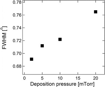
Figure 1 shows a typical 2θ–ω diffraction pattern of the ScN(001) thin film sputtered onto the MgO(001) substrate at 5 mTorr. Only the (002) ScN diffraction reflection was observed. The position of the 002 peak corresponds to 4.50 Å, a relaxed lattice constant of ScN in the growth direction. An epitaxial growth of the ScN thin film on the MgO substrate with cube-on-cube relationship of ScN(001)[100]║MgO(001)[100] was confirmed using the results of φ-scans for (111) MgO and (111) ScN reflections, shown in the inset of Fig. 1. Films deposited at 2, 10, and 20 mTorr show similar diffraction patterns and exhibit the same epitaxial relationships with respect to the MgO substrate. Figure 2 shows a full-width-at-half-maximum (FWHM) of the 002 ScN rocking curves as a function of the deposition pressure. FWHM values increase from 0.691 to 0.765° as the deposition pressure raises from 2 to 20 mTorr, respectively, indicating slight degradation of the crystal quality of the ScN film.
2θ–ω XRD pattern obtained from the ScN thin film deposited at 5 mTorr. The inset is the phi scan revealing the cube-on-cube epitaxial relationship between the ScN film and MgO substrate.

FWHM of 002 rocking curves for ScN films deposited at 2, 5, 10, and 20 mTorr, respectively. The FWHM increases with the raise of the deposition pressure.

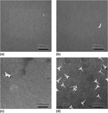
While there is no apparent variation in the 2θ–ω XRD patterns for ScN films deposited at different deposition pressures, their surface morphologies differ significantly. High-resolution SEM images of the surfaces of the ScN films as a function of the deposition pressure are presented in Fig. 3. The surface morphology of the ScN thin films grown at low deposition pressure—2 [Fig.3(a)] and 5 mTorr [Fig. 3(b)]—is composed of square flat-topped densely packed mounds. The sides of the mounds are oriented along (001) planes that are consistent with expected 4-fold symmetry of the rocksalt ScN. The characteristic mound lateral size increases with the deposition pressure from about 40 to 60 nm for ScN thin films grown at 2 and 5 mTorr, respectively. The surface mound structure of the ScN thin film deposited at 10 mTorr becomes less organized and nonuniform, as can be seen in Fig. 3(c). The lateral mound size fluctuates in the range of 60–200 nm. The shape of the large mounds becomes square with straight sides and sharp corners. The large square features become more pronounces as the deposition pressure reaches 20 mTorr [Fig. 3(d)]. As it is evident from the SEM image, there is a high density of secondary triangle-shaped grains that were not picked up by the XRD scan.
SEM images of the ScN thin films deposited at (a) 2, (b) 5, (c) 10, and (d) 20 mTorr, respectively. The surface morphology shows a strong dependence on the deposition pressure.

The formation of a mound structure is commonly observed on the surfaces of single-crystal ScN thin films Reference Gall, Petrov, Hellgren, Hultman, Sundgren and Greene4,Reference Burmistrova, Maassen, Favaloro, Saha, Salamat, Koh, Lundstrom, Shakouri and Sands10,Reference Gall, Petrov, Desjardins and Greene29 as well as in some other transition metal nitrides, semiconductors, and metals. Reference Stroscio, Pierce, Stiles, Zangwill and Sander30–Reference Ehrlich and Hudda33 On stepped surfaces, the downstep motion of an adatom laying in the vicinity of the step edge is inhibited by the Ehrlich–Schwoebel barrier Reference Ehrlich and Hudda33–Reference Golzhauser and Ehrlich35 resulting in a preferential uphill migration, thereby promoting nucleation on terraces. Depending on the magnitude of the barrier (which is a function of the substrate temperature), the degree of kinetic surface roughness and faceting varies. Reference Leal, Ferreira and Ferreira36 In the case of the ScN thin films being described herein, the substrate temperature was maintained at 650 °C, a temperature that is relatively high to provide sufficient adatom mobility to suppress the surface roughening. However, the regular arrays of mounds with a subnanometer height are still observed to form in the high-pressure films.
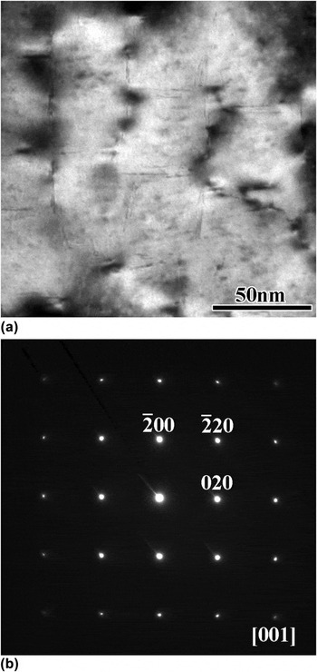
As can be seen in a plan-view TEM image in Fig. 4(a), nanopipes develop in the cusps surrounding the mounds, due to the atomic shadowing which causes a reduced deposition rate. This structure was previously observed in sputtered ScN thin films. Reference Gall, Petrov, Hellgren, Hultman, Sundgren and Greene4,Reference Burmistrova, Maassen, Favaloro, Saha, Salamat, Koh, Lundstrom, Shakouri and Sands10,Reference Gall, Petrov, Desjardins and Greene29 In addition to nanopipes, arrays of dislocations form to accommodate the approximately 7% lattice mismatch between the MgO(001) substrate and the ScN(001) thin film. Figure 4(b) presents a selected area electron diffraction (SAED) pattern obtained along the [001] zone axis of the ScN thin film deposited at 2 mTorr. Based on the evaluation of the high-order diffraction spots, a high crystal quality of the ScN material is confirmed.
(a) Plan-view TEM image of the ScN thin film sputtered at 2 mTorr and (b) SAED.

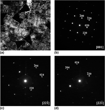
A dark field TEM image of the ScN film deposited at 20 mTorr prepared in a plan-view configuration is shown in Fig. 5(a). As was detected by SEM [Fig. 3(c)], triangle-shaped grains grow through the ScN(001) matrix. The mound boundaries internal to the film become more diffused and pronounced. This type of contrast may arise from defects running at an angle to the film surface. These defects do not reveal themselves in a SAED pattern taken from the area of the film of about 50 nm that is free of secondary grains [Fig. 5(b)]. The SAED is typical for single crystal ScN(001) and similar to one taken from the ScN thin film deposited at 2 mTorr [Fig. 4(b)]. The secondary grains exist in two distinct orientations rotated 90° with respect to each other. The orientation of the grains of
 $\left[ {2\bar 21} \right]$
and
 $\left[ {22\bar 1} \right]$
, respectively, is obtained from analysis of SAEDs [Figs. 5(c) and 5(d)] taken from the two perpendicular grains. This type of reflections is forbidden for the face centered cubic (FCC) lattice of the rocksalt ScN explaining the absence of reflections corresponding to secondary grains in the 2θ–ω XRD pattern.
(a) Dark field plan-view TEM image of the ScN thin film deposited at 20 mTorr. Secondary grains form within the ScN(001) epitaxial film. (b) SAED obtained from the area of the film free from secondary grains. (c) and (d) SAEDs obtained from a pair of secondary grains perpendicular to each other. The secondary grains are of <221> type.

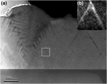
To study the inclined defects present in the plane view image [Fig. 5(a)], a cross-sectional sample was made through a secondary grain with a <221> type orientation; therefore, these defects can be imaged edge-on. Figure 6(a) shows a high angle annular dark field (HAADF) STEM image of the ScN thin film deposited at 20 mTorr. The inclined defects are clearly visible as dark lines running at an angle of about 60° with respect to the substrate surface. EELS mapping acquired from the area marked in Fig. 6(a) reveals the presence of oxygen [Fig. 6(b)]. Thus, during the deposition, oxygen is partially expelled from the ScN lattice and concentrates on the defects and grain boundaries, thereby potentially affecting electronic properties of ScN thin films deposited at 20 mTorr.
(a) HAADF cross-sectional STEM image of the ScN thin film deposited at 20 mTorr. The cross-section is taken through the secondary grain that is clearly seen on the left. Defects inclined about 60° with respect to the surface form. (b) EELS mapping from the defect showing the oxygen accumulation.

The evolution of the surface morphology during a film growth is mainly defined by the surface mobility of the adatoms and expected to strongly depend on substrate temperature and the flux of impinging particles or the deposition rate. All ScN thin films were deposited at the same substrate temperature of 650 °C. Therefore, the flux of the incoming particles including neutrals and plasma ions as well as their energies plays a major role in the structural evolution of the ScN films. At 2 mTorr, the mean-free-path (MFP) traveled by a particle before a collision event is about 2.5 cm, which is about one-fourth of the distance between the Sc target and the substrate in the used sputter configuration. Thus, the sputtering proceeds within an almost ballistic regime. In comparison, at 20 mTorr the MFP is an order of magnitude smaller. In addition, the high-energy bombardment enhances adatom mobility, and thus the surface planarization, thereby promoting the growth of high-quality, single-orientation epitaxial ScN thin films.
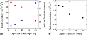
Figure 7 shows the electrical resistivity, electron mobility, and carrier concentration as a function of deposition pressure obtained from the room temperature Hall measurements in the van der Pauw configuration. All samples showed n-type semiconducting behavior. The ScN thin film deposited at 2 mTorr yields the highest mobility value of 98 cm2 V−1 s−1. The electron mobility decreases with increasing deposition pressure to 20 mTorr, reaching a value of 29 cm2 V−1 s−1. The electrical resistivity exhibits the opposite trend, increasing by almost an order of magnitude from 0.2 to 1.9 mΩ cm for ScN thin films deposited at 2 and 20 mTorr, respectively. The increase in electrical resistivity and the reduction of the electron mobility may be attributed to the enhanced defect scattering, as we have shown that the film crystallinity degrades as the deposition pressure goes up.
(a) Electrical resistivity (blue diamond) and electron mobility (red circle), and (b) electron concentration of the ScN thin films as a function of the deposition pressure.

The measured values of the carrier concentration are in the degenerate range for all samples. Figure 7(b) shows a slight reduction of the carrier concentration with increasing deposition pressure (from 2.5 × 1020 cm−3 to 1.2 × 1020 cm−3). The degenerate behavior of ScN is attributed to the oxygen contamination during the ScN thin film sputter deposition. Reference Burmistrova, Maassen, Favaloro, Saha, Salamat, Koh, Lundstrom, Shakouri and Sands10,Reference Moram, Novikov, Kent, Nörenberg, Foxon and Humphreys12 Even at a base pressure approaching ultra high vacuum deposition conditions, an oxygen incorporation of about 1% occurred. Oxygen forms a solid solution within ScN and acts as a donor. Reference Burmistrova, Maassen, Favaloro, Saha, Salamat, Koh, Lundstrom, Shakouri and Sands10,Reference Kerdsongpanya, Alling and Eklund16 This unintended doping leads to a shift of the Fermi energy toward and into the conduction band (known as the Burstein–Moss shift Reference Burstein37 ) resulting in an apparent increase of the band gap. The incorporation of oxygen at a concentration of about 1% appears to be advantageous in improving thermoelectric properties of ScN thin films. Reference Burmistrova, Maassen, Favaloro, Saha, Salamat, Koh, Lundstrom, Shakouri and Sands10 While oxygen gets incorporated into the ScN lattice for samples grown at low deposition pressure, the increase of pressure to 20 mTorr leads to the accumulation of some oxygen on the grain boundaries and defects, thereby excluding it from the host lattice and minimizing its effect on the conduction properties of the films [see Fig. 6(b)].
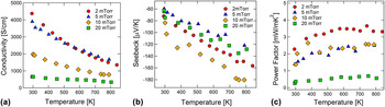
The temperature dependent in-plane electrical conductivity, in-plane Seebeck coefficient, and power factor of ScN thin films deposited at various deposition pressures are shown in Fig. 8. For all samples, the electrical conductivity [Fig. 8(a)] decreases with increasing temperature. The magnitude of the decrease is the lowest for the sample grown at 20 mTorr. At 800 K, the electrical conductivity reaches values of 1504, 1679, 784, and 340 S/cm for ScN thin films deposited at 2, 5, 10, and 20 mTorr, respectively. The magnitude of Seebeck coefficient [Fig. 8(b)], on the other hand, increases with increasing temperature. The highest value of the Seebeck coefficient (−180 at 800 K) was recorded for the ScN film grown at 10 mTorr. For all films, the values of the Seebeck coefficient are in the −120–180 µV/K range, values that are among the highest ever reported for ScN thin films.
Temperature dependent (a) electrical conductivity, (b) Seebeck coefficient, and (c) power factor of ScN thin films deposited at 2, 5, 10, and 20 mTorr.

The power factor also increases with increasing temperature [Fig. 8(c)]. However, it saturates after about 600 K for all ScN films. The ScN thin film deposited at 2 mTorr showed the maximum power factor, 3.3 W/mK2 at 800 K. As the deposition pressure increases, the power factor decreases, reaching 2.55 and 2.50 W/mK2 at 800 K for films grown at 10 and 5 mTorr, respectively. The lowest value of the power factor of 0.56 W/mK2 at 800 K was obtained for the ScN film deposited at 20 mTorr.
IV. CONCLUSIONS
The effect of deposition pressure on the structural and thermoelectric properties of ScN thin films deposited by the reactive magnetron sputtering onto MgO(001) substrates has been studied. Deposition pressure plays a key role in determining the crystallinity, surface morphology, and defect character of the sputtered ScN films, as well as the electric and thermoelectric properties. The microstructural and thermoelectric properties of the ScN thin films degrade with increasing deposition pressure. The ScN thin films deposited at 2, 5, and 10 mTorr are single crystalline epitaxial thin films and as a result, they exhibit superior electric and thermoelectric properties. A power factor of 3.3 W/mK2 at 800 K was obtained for the ScN thin film sputtered at 2 mTorr. For ScN thin films sputtered at 5 and 10 mTorr, the values of the power factor were about 2.5 W/mK2 at 800 K, a value that is still among the highest values for ScN. The deposition at 20 mTorr leads to a significant degradation of the crystallinity and formation of the secondary 221-oriented grains. Additionally, oxygen partially concentrates on the defects and grain boundaries in these films, leading to a decrease in the carrier concentration as well as in the electrical conductivity. As a result, the ScN thin films deposited at 20 mTorr demonstrate a reduction of the power factor to 0.5 W/mK2 at 800 K. It is, thus, apparent that maintaining a deposition pressure below 10 mTorr provides desirable conditions for the formation of ScN thin films with advanced properties.
ACKNOWLEDGMENTS
This work was funded by DARPA/Army Research Office Contract No. W911NF0810347. Research carried out in part at the Center for Functional Nanomaterials, Brookhaven National Laboratory, which is supported by the U.S. Department of Energy, Office of Basic Energy Sciences, under Contract No. DE-AC02-98CH10886.