I. INTRODUCTION
Cu has replaced Al as Back End of Line (BEOL) interconnects due to its low electrical resistivity and superior electromigration (EM) reliability. Compared with Al, Cu has a distinct EM failure mechanism due to its different mass transport characteristics. While the mass transport in Al interconnects comes mainly from grain-boundary diffusion, in submicron Cu interconnects, it is dominated by diffusion along the Cu/SiNx cap interface.Reference Hu, Rosenberg and Lee1 Although scaling will degrade the EM lifetime of both Al and Cu interconnects since less void volume will be required to induce EM failure, the effect will depend on the specific mechanism dominating the mass transport. For submicron Cu interconnects, the EM lifetime degrades by half for each new technology node, even with the same current density.Reference Hu, Gignac and Rosenberg2 This has stimulated great interests in modifying the Cu/SiNx interface by using a metal cap layerReference Hu, Gignac, Rosenberg, Liniger, Rubino, Sambucetti, Domenicucci, Chen and Stamper3–Reference Aubel, Thierbach, Seidel, Freudenberg, Meyer, Feustel, Poppe, Nopper, Preusse, Zistl and Weide-Zaage7 to suppress the interfacial mass transport and improve EM reliability. The CoWP cap was found to be particularly effective, yielding two orders of magnitude improvement in the EM lifetime at the test temperature.Reference Hu, Gignac, Rosenberg, Liniger, Rubino, Sambucetti, Stamper, Domenicucci and Chen4, Reference Aubel, Thierbach, Seidel, Freudenberg, Meyer, Feustel, Poppe, Nopper, Preusse, Zistl and Weide-Zaage7 However, the EM lifetime statistics was found to degrade with the application of the CoWP capping, and the EM improvement seemed to vary with the manufacturing process,Reference Aubel, Thierbach, Seidel, Freudenberg, Meyer, Feustel, Poppe, Nopper, Preusse, Zistl and Weide-Zaage7–Reference Christiansen, Li, Angyal, Kane, McGahay, Wang and Yao9 suggesting a metallization with great potential for future interconnects but difficult to implement. A recent study by Hu et al. showed that, for Cu interconnects narrower than 90 nm, small grains agglomerated and mixed with large bamboo grains.Reference Hu, Gignac, Baker, Liniger, Yu and Flaitz10 The EM lifetime was found to be degraded further due to an increase in the grain boundary contribution to mass transport. In another recent study, void formation and evolution was examined for CoWP-capped samples using in situ scanning electron microscopy (SEM) where the microstructure, particularly the agglomeration of mixed size grains was found to be important for void nucleation and growth.Reference Meyer and Zschech6, Reference Zschech, Ho, Schmeisser, Meyer, Vairagar, Schneider, Hauschildt, Kraatz and Sukharev11 Together these studies raise an interesting and basic question regarding the extent of the grain structure effect on the EM lifetime and statistics for Cu interconnects with CoWP capping. This question is important for future development of the metal cap layer, in particular CoWP, for improving the EM performance as scaling continues for Cu interconnects.
In this article, we investigated the grain structure effect on EM lifetime, statistics, and void formation by performing statistical EM tests and failure analysis on CoWP-capped Cu interconnects with different grain sizes.
II. EXPERIMENTAL DETAILS
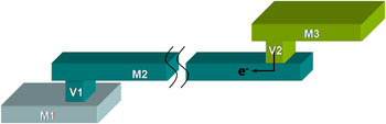
The test structure used in this study was a single-linked EM structure consisting of three-level interconnects as shown in Fig. 1. The nominal dimensions of the M2 test line were 72 nm wide, 144 nm thick, and 200 μm long. The M1 and M3 feeder lines were made wider and shorter to minimize the EM failure probability in these lines. The structures were fabricated by GLOBALFOUNDRIES using a standard damascene process (Milpitas, CA). The Cu interconnects were surrounded by Ta-based liner at trench/via sidewalls and bottom interfaces, and capped with SiCN-based dielectric layer on the top. For the M2 line, a thin CoWP capping (∼6 nm thick) was applied prior to the SiCN cap deposition. By tuning the current-profile during electroplating, two different grain sizes, large and small grains, were obtained at the M2 level for studying the grain size effect. Downstream (M3-V2-M2) package level EM tests were carried out at the temperature of 330 °C and a current density of 1.05 MA/cm2 in the M2 test line. The EM lifetime was determined at 10% resistance increase. Dual-beam focused ion beam/SEM and transmission electron microscopy (TEM) were used to characterize the Cu microstructure and identify the voiding location.
Schematic diagram of three-level downstream electromigration (EM) test structure. M2 line is the test line.

III. RESULTS AND DISCUSSION
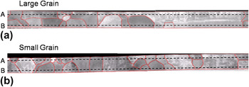
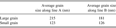
Figure 2 shows the cross-sectional TEM images along the Cu line direction of the two sets of Cu lines with different grain sizes. Both lines reveal a “near bamboo” grain structure with bamboo segments mixing with polycrystalline segments. The grain size analysis was performed near the trench top and bottom, and the results were summarized in Table I. The results clearly identify the grain size difference between these two sets of Cu lines, which will be referred to as “large grain” and “small grain” structures in the following discussion.
Longitudinal transmission electron microscopy (TEM) images of M2 Cu line with different grain structures: (a) large grain, (b) small grain. The grain size was determined along the dashed lines A and B.

Average grain length for large and small grain structures along the dashed line A and line B in Fig. 2.

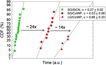
The cumulative distribution function (CDF) plots for test structures with large and small grains are shown in Fig. 3. To show the CoWP capping effect, we include the CDF plot for the small grain structures with the standard SiCN cap, which were fabricated under identical conditions as the CoWP-capped small grain structures. By comparison, it is clear that both CoWP small grain and large grain structures show significant improvements of the EM lifetime, about 24× for the small grain structures and another ∼14× for the large grain structures. Since the cap layer deposition processes for both sets of CoWP-capped structures were identical, we can assume that the mass transport along their respective cap interfaces is the same. Therefore, the shorter EM lifetime for the small grain structures can be attributed to the additional grain boundary contribution to the mass transport. Previously, Hau-Riege et al. reported that for a very weak Cu/cap interface where the cap interface diffusion was much faster than the grain-boundary diffusion, the effect of microstructure was negligible with a similar EM lifetime observed for Cu lines with bamboo-like and polycrystalline structures.Reference Hau-Riege and Thompson12 However, when the cap interface was improved, the Cu microstructure was found to start impacting the EM lifetime.Reference Hu, Gignac, Baker, Liniger, Yu and Flaitz10 In this study, the significant lifetime improvement observed for the large grain structures with CoWP capping compared to the small grain structures indicates that diffusion along grain boundaries can become significant in contributing to the overall mass transport when the interface diffusion is effectively suppressed.
Cumulative failure probability plots of EM tests for CoWP-capped Cu interconnects with different grain sizes. The result for SiCN-capped small grain structures is included as a comparison. Here, “SG” refers to small grain and “LG” refers to large grain. EM test was performed at 330 °C and 1.03 MA/cm2.

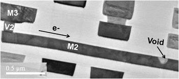
Failure analysis showed that for both large and small grain structures, voids mostly formed in the trench away from the cathode via, as shown in Fig. 4. This is different from the SiCN cap, where voids usually form right at the cathode via.Reference Oates and Lee13 During EM, voids nucleate at flux divergence sites, where an unbalanced Cu flow rate exists. For downstream EM, the cathode via corner is a major flux divergence site because the Ta barrier at the cathode via bottom blocks the Cu atoms in the via from diffusing down to the trench line. Another flux divergence site is the interface/grain boundary intersection (triple junction point) due to the grain structure-induced Cu diffusivity variation. In situ EM study shows that, after void nucleation, voids either get trapped at the nucleation sites or migrate toward the cathode end of the line.Reference Zschech, Ho, Schmeisser, Meyer, Vairagar, Schneider, Hauschildt, Kraatz and Sukharev11, Reference Hauschildt, Gall, Thrasher, Justison, Michaelson, Hernandez, Kawasaki and Ho14 For Cu interconnects with CoWP capping, Cu diffusion along the cap interface is significantly suppressed due to the strong Cu/Co bonding. Consequently, Cu grain boundaries and Cu/liner interfaces are more involved in the diffusion process. Once a relatively large void is nucleated and formed at a triple junction point, the energy required for void migration along the Cu line is significant. Thus, the void is more likely to get trapped at the nucleation site, then merges with other small voids to cause the interconnect failure. This is different from the SiCN cap, for which the atomic diffusion along the cap interface is much faster. After a void is nucleated and formed at the triple junction, it can move more readily along the interface and eventually accumulate at the cathode via. As a result, most SiCN-capped Cu interconnects show a final void located at the cathode end after EM stressing.
TEM image of a focused ion beam cross-sectioned sample showing void formation in the trench several microns away from the cathode via.

Turning to the EM statistics, it is important to point out that the statistical variation σ for the CoWP-capped structures (σ = 0.88 ± 0.33 for large grains, σ = 0.53 ± 0.06 for small grains) is considerably larger than for the SiCN-capped structures (σ = 0.27 ± 0.02). For Cu interconnects with the CoWP capping, considerable variations in the EM lifetime improvement and statistics have been reported, where a large sigma was commonly observed, especially for the upstream via depletion EM stressing.Reference Gall, Hauschildt, Justison, Ramakrishna, Hernandez, Herrick, Michaelson, Kawasaki, Tsui, Joo, Michaelson, Lane and Volinsky8, Reference Christiansen, Li, Angyal, Kane, McGahay, Wang and Yao9 So far, the cause of the large sigma remains unclear although it has been attributed to the difficulty in fabricating a uniform and thin CoWP layer on top of Cu interconnects and the sidewall voiding in the via.Reference Gall, Hauschildt, Justison, Ramakrishna, Hernandez, Herrick, Michaelson, Kawasaki, Tsui, Joo, Michaelson, Lane and Volinsky8, Reference Christiansen, Li, Angyal, Kane, McGahay, Wang and Yao9
In addition to the different EM statistics of the SiCN-capped and CoWP-capped structures, the grain structure was found to influence the EM statistics for the CoWP-capped structures. Although there was considerable uncertainty in the sigma of the large grain structure due to the limited data points, the statistics showed a larger sigma (0.88 ± 0.33) for the large grain structure than the small grain structure. For Cu interconnects with CoWP capping, with the interface diffusion effectively suppressed, the contribution from grain boundaries to the mass transport clearly became important and was found to have a significant effect on the EM lifetime and statistics in this study.
Similar grain structure effects have been observed for Al(Cu) interconnects, and a statistical model based on the grain structure distributions has been formulated to account for the EM lifetime and statistics.Reference Cho and Thompson15–Reference Korhonen, Borgesen, Brown and Li17 This model considered the statistical distribution of the grain structure in a line consisting of bamboo and polycrystalline grain segments connected in series and applied the weakest-link model to calculate the EM lifetime and statistics based on the rate of void formation due to the Blech effect. We have extended this model to account for the grain structure effect on the EM lifetime and statistics for CoWP-capped Cu interconnects. The results will be reported later in another paper.
IV. CONCLUSIONS
In summary, the grain structure effect on EM reliability for Cu interconnects with CoWP capping has been investigated. Two sets of Cu lines with different grain sizes were fabricated by tuning the process parameter during electroplating with otherwise identical processing. The large grain structures showed a longer EM lifetime compared with the small grain structures. The reduced lifetime for the small grain structures was attributed to an increase in the grain-boundary diffusion, which is much faster than the Cu/CoWP cap interface diffusion. Failure analysis identified that voids mostly formed in the trench some distance away from the cathode via for both structures. The effect of the grain structure on EM lifetime statistics was also observed for the CoWP capping structures, particularly when the statistics are compared to that of the SiCN capping structures. The results show that for Cu interconnects with CoWP capping suppressed interface diffusion, the microstructure can play a key role in controlling the degradation mechanism, EM lifetime, and statistics. For future technology node, when Cu lines degrade from bamboo-like to polycrystalline structure, it is critical to control the grain size and microstructure to ensure the EM reliability.
ACKNOWLEDGMENTS
This work is partially supported by the Center for Advanced Interconnect Science and Technology of the Semiconductor Research Cooperation (CAIST/SRC). The authors would also like to acknowledge GLOBALFOUNDRIES at Dresden, Germany for providing the test structures.