Introduction
Metalorganic Chemical Vapour Deposition (MOCVD) growth of Gallium Nitride (GaN) in the [000 ] direction is associated with the formation of surface defects, such as hexagonal hillocks [Reference Seelmann-Eggebert, Weyher, Obloh, Zimmermann, Rar and Porowski1,Reference Ponce, Bour, Young, Saunders and Steeds2,Reference Rouvière, Arlery, Niebuhr, Bachem and Briot3]. The inversion domain, located at the centre of the point-topped pyramids, apparently causes hillock formation as a result of the higher growth rate of this defect compared with the growth rate of the surrounding matrix [Reference Rouvière, Arlery, Niebuhr, Bachem and Briot3]. Also for homo-epitaxial growth on the N-side of GaN substrates formation of hexagonal pyramids is observed [Reference Weyher, Brown, Zauner, Müller, Boothroyd, Foord, Hageman, Humpreys, Larsen, Grzegory and Porowski4,Reference Brown, Weyher, Boothroyd, Foord, Zauner, Larsen, Hageman, Bockowski and Humphreys5].
Homo-epitaxial growth in the [000 ] direction has the advantage that the N-side of GaN single crystals can be mechano-chemically polished to obtain epi-ready substrates [Reference Weyher, Müller, Grzegory and Porowski6], while the Ga-side (for growth in the [0001] direction) can only be mechanically polished, so that reactive ion etching is needed to prepare epi-ready substrates [Reference Schauler, Eberhard, Kirchner, Schwegler, Pelzmann, Kamp, Ebeling, Bertram, Riemann, Christen, Prystawko, Leszczynski, Grzegory and Porowski7].
For device applications smooth surfaces are required, therefore the formation of hillocks should be avoided. A common way to avoid growth features on the surface is the use of misoriented substrates [Reference van Enckevort, Janssen, Vollenberg and Giling8]. In the present work the surface morphology of homo-epitaxial GaN layers is studied for different off-angle orientations from the exact [000 ] direction. It is found that the formation of hexagonal pyramids can be strongly suppressed by the use of a sufficiently large misorientation, resulting in much smoother layers.
Experimental
GaN single crystals [Reference Porowski9] were used as substrates for MOCVD growth. The (000 ) substrate surfaces were mechano-chemically polished [Reference Weyher, Müller, Grzegory and Porowski6] to obtain off-angle orientations of 0°, 2°, and 4° towards the [10
 0] direction. The misorientation was confirmed by X-ray diffraction analysis.
Homo-epitaxial GaN growth was performed at a temperature of 1040°C and a pressure of 50 mbar using trimethylgallium (TMG) and ammonia (NH3) as precursors, and hydrogen (H2) as carrier gas. The substrate crystals were heated to growth temperature under a NH3 gas flow diluted in nitrogen (N2). Growth was performed with a V/III molar ratio of about 1700 with a total flow of about 5 slm.
The surfaces of the homo-epitaxial GaN layers were investigated by optical differential interference contrast microscopy (DICM), a technique very sensitive for detecting local differences in surface slope, which are visualised by different shades of grey in the figures.
Results and Discussion
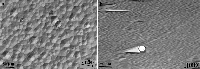
Optical examination with DICM of layers grown on (000 ) substrates without misorientation reveals a large number of hexagonal growth hillocks covering almost the entire surface. As shown in figure 1a the hexagonal base of the hillocks is 10-50 μm in size. The majority of the hillocks are regular point-topped pyramids, although some of them are macroscopically flat-topped or disrupted. The highest hillocks, with steeper side facets, show an increased contrast. Similar hillock morphology has been observed for hetero-epitaxial GaN layers grown in the [000
 ] direction [Reference Rouvière, Arlery, Niebuhr, Bachem and Briot3,Reference Romano and Myers10]. Faster growing inversion domains of Ga-polarity in a matrix of N-polarity lead to the formation of hillocks [Reference Rouvière, Arlery, Niebuhr, Bachem and Briot3]. Also for homo-epitaxial growth on the N-side hexagonal pyramids were observed [Reference Weyher, Brown, Zauner, Müller, Boothroyd, Foord, Hageman, Humpreys, Larsen, Grzegory and Porowski4,Reference Brown, Weyher, Boothroyd, Foord, Zauner, Larsen, Hageman, Bockowski and Humphreys5].
DICM image of a homo-epitaxial GaN layer grown on the N-side (000 ) of a GaN single crystal (a)without misorientation and (b) 4° misorientation towards the [10
 0] direction.

The virtual (000 ) plane, of macroscopically flat-topped pyramids, is faceted due to steps generated by a step source located at the centre of the hexagon. These steps originate from dislocations at the centre of such hillocks, as was concluded from the occurrence of interlaced spirals with atomic height steps [Reference Nowak, Pakula, Grzegory, Weyher and Porowski11].
For the sample with a 2° off-angle orientation towards the [10 0] direction the density of hillocks at the surface is significantly lower compared to the exactly oriented samples (see table I). The misorientation induced step flow started to overgrow part of the hexagons. However, for the majority of the features on the surface the source of growth is still present. The step flow resulting from the 2° misorientation appeared to be insufficient to overgrow the centres of the hillocks.
The dependence of the hillock density on the misorientation of the GaN substrates.
| misorientation (°) | hillock density (cm−2) |
| 0 | 1.2E+05 |
| 2 | 2.8E+04 |
| 4 | 1.3E+03 |
The estimated hillock density for the 4° misoriented specimen is nearly two orders of magnitude lower as compared with specimens of exact orientation (see table I). Obviously the step flow resulting from the misorientation, which is doubled compared to the 2° off-angle sample discussed above, is sufficient to overgrow the centres of the majority of the hexagons.
Although, for 4° misorientation most hexagonal features disappeared from the surface (figure 1b), there is still a number of partial and complete hexagonal hillocks that can be recognised. A number of these features is shown in figure 2. Figure 2a shows a kind of plateau with a partly overgrown hexagonal hillock near its centre, dividing the plateau in two parts. The two regions, which border on the edges of the hillock, are not equally sized. From the difference in size of those two areas it can be concluded that the misorientation is not exactly in the [10 0] direction. The plateau ends abruptly in a steep step bunch perpendicular to the [10
 0] direction. In figure 2b a part of a hexagon can still be recognised. Like the hillock shown in figure 2a, the two side areas that border on the hexagon are not equal in size and the plateau terminates in the [10
 0] direction resulting in a sharp, steep edge. For the feature shown in figure 2c a discontinuity in slope of the plateau itself can be recognised at the place where the plateau starts to narrow. On the plateaus of the surface features of figure 2a-2c steps sloping towards the <11
 0> directions can be seen.
DICM images of different surface features found after growth on the 4° misoriented single crystal. The arrow in c) indicates the discontinuity line on the plateaus. d)The feature indicates a fluctuation in activity of the growth centre during growth.

A plausible explanation for the occurrence of the surface features shown in figure 2 can be given. The sample was mechano-chemically polished to a 4° misorientation, thereby introducing steps approximately parallel to [ 2 0], over the sample. At the beginning of growth shallow as well as steep hexagonal hillocks tend to be formed. However, only steep hexagonal hillocks, which are formed by a more active step source, survive the propagation of the misorientation step train and will be present after a certain period of growth (see figure 2). Less steep hillocks are overgrown in an early stage of the process or cannot be formed at all. In figure 1a it can be seen that the height of the hillocks varies over the sample. About 3% of the hillocks presented in figure 1a show an enhanced contrast which indicates steeper hillocks. This percentage is in agreement with the previous observation of the reduced hillock density by almost two orders of magnitude for the 4° misoriented sample as compared with the samples without misorientation.
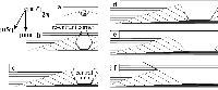
In addition, the activity of many individual hillocks decreases or fluctuates during growth (see figure 2d). If the activity of the step source at the hillock centre decreases vertical growth slows down but the base of the hillock still expands. The time dependent overgrowth of a steep hillock of which the vertical growth is suddenly almost stopped is represented schematically in figure 3.
Schematic representation of the time-dependent development and subsequent overgrowth of a hexagonal hillock. Image a) is two times enlarged. The arrow in f) indicates the discontinuity line on the plateau, cf.figure 2c.

In its steep period as well as in its first time of slow vertical growth the slowest advancing steps, in the <10  0> directions, bound the hillock (figure 3a). The steps introduced by the misorientation are more or less in the [10
 0] direction, which means that these steps also move slowly. Steps in other directions move considerably faster. Steps from the left and right hand side of the hillock form a re-entrant corner with the steps induced by the misorientation (see figure 3). Due to an increased effective supersaturation near this region the step velocity increases and the re-entrant corner becomes rounded [Reference Van der Hoek, Van der Eerden and Bennema12]. Now a whole range of step orientations is created, and steps in the fast moving <11
 0> directions are selected to propagate over the plateaus.
Figure 3b represents a hillock of which the step source has already been inactive for some time at the moment that the misorientation-induced steps just start to overgrow the flat top of the hillock. The steps on the plateau, left and right from the hillock, move faster than the steps introduced by the misorientation. During continued growth the hexagoncentre will be overgrown (figure 3d-3e).
From the moment that the hillock is half overgrown, and no steps opposite to the misorientation-steps exist (figure 3d), the position of the re-entrant corner moves along the intersection line of the remaining hillock side facet and the plateau during prolonged growth (figure 3e) and will finally evanesce (figure 3f). The boundary between the stepped plateau areas and the central region of the plateau, which is more or less parallel to the (000 ) plane, now corresponds with the last fast <11
 0> step emitted from the vanishing hillock, cf. figure 2c.
From the mechanism of hillock overgrowth shown in figure 3 it becomes also clear that as long as the hillock, or part of it, is present on the surface the plateaus next to the hillock become wider along <10  0>. Since the plateaus are formed from steps emerging from the re-entrant corner, the plateaus were narrower at earlier times of growth when the hillocks were smaller. This explains the triangular shape of both plateaus parts adjacent to the hillocks and the fact that the hillock is more or less located at the centre of the plateau.
During continued growth and assuming that the steps at the steep edge of the plateau propagate as fast as the misorientation steps, the plateau expands in the left and right directions, only due to expansion of the flat central area. Apart from translation the stepped triangular plateau regions do not change in time (figure 3).
The moment at which the situation represented in figure 3b occurs during the growth process depends on the time-dependent activity of the growth source of the hillock during the earlier stage of the growth run, which is different for the individual hillocks. Therefore, different stages of feature development appear side by side on the same layer after a certain period of growth as shown in figure 2. A hillock of which the step source has become inactive at a very early stage of growth will be overgrown much faster, i.e. the time between the different stages of the overgrowth process presented in figure 3 will be much shorter. Overgrowth of the hillock will also be faster for higher misorientations towards the [10 0] direction and same step source activity of the hillock. Overgrowth of the remaining part of the hillock can only be realised if steps introduced by the misorientation move faster than the steps of the remainder of the hillock.
Steps in the <11  0> directions move 2.5 times as fast as steps in the <10
 0> directions, as is determined by measuring the distances between the small step bunches on both the misoriented surface and the plateau. Therefore, a misorientation towards the [11
 0] direction should be chosen in order to overgrow the surface features completely.
Conclusions
During MOCVD growth of GaN films on the N-side of exactly oriented GaN single crystal substrates, hexagonal pyramids are formed. In this study it is found that the formation of these pyramids can be largely suppressed by the use of substrates with a slight misorientation towards the [10 0] direction. For a substrate misorientation of 4° the density of the elevations on the homo-epitaxial film is reduced by almost two orders of magnitude as compared with exactly oriented GaN substrates. The morphologies of those features that persist on the 4° off-angle sample during growth can be explained by a model involving the interaction of steps introduced by the misorientation with steps originating from the hillocks.
It is found that the step velocity is dependent on the step orientation: steps in the <11  0> directions move 2.5 times as fast as steps in the <10
 0> directions.
Considerations following from the model indicate that for a further improvement of the surface morphology by reduction of the hillock density either substrates with larger misorientations or, since the step velocity is highly anisotropic, with misorientations towards the [11 0] direction are needed.
Acknowledgements
This work was financially supported by the Dutch Technology Foundation (STW). JLW wishes to thank for the grant of NATO Scientific Affair Division.