I. INTRODUCTION
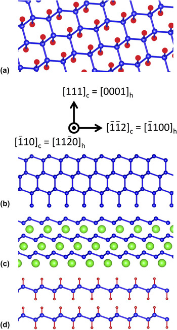
The discovery and mechanical exfoliation of single layer graphene has led to a revolution in nanoscale materials science by enabling a plethora of new physics and chemistry in two dimensions (2D) that is not possible in conventional three-dimensional materials. Reference Novoselov, Geim, Morozov, Jiang, Katsnelson, Grigorieva, Dubonos and Firsov1–Reference Geim and Novoselov3 Beyond graphene, there is great interest in exploring 2D materials that offer properties not found in graphene, such as a native band gap, strong spin–orbit coupling, and strong exciton confinement. Reference Butler, Hollen, Cao, Cui, Gupta, Gutierrez, Heinz, Hong, Huang, Ismach, Johnston-Halperin, Kuno, Plashnitsa, Robinson, Ruoff, Salahuddin, Shan, Shi, Spencer, Terrones, Windl and Goldberger4 Of particular interest is germanane (GeH), the germanium-based analogue of graphane (CH), which has recently been synthesized as a bulk single-crystal and exfoliated onto insulating substrates. Reference Bianco, Butler, Jiang, Restrepo, Windl and Goldberger5 This was achieved by first synthesizing bulk crystals of layered Zintl-phase CaGe2, then submerging the crystals in hydrochloric acid (HCl) to de-intercalate the Ca atoms (Fig. 1). This results in stacked layers of 2D germanane sheets, where each sheet consists of Ge atoms arranged in a buckled honeycomb lattice and sp 3-hybridized due to covalent bonds to hydrogen as shown in Fig. 1(a).
(a) Atomic structure diagram of germanane (GeH). (b) Projected view of the bulk germanium lattice. The axis indicates the directions within the cubic lattice and in the corresponding hexagonal lattice (for CaGe2 and germanane). (c) Projected view of CaGe2 films. (d) Projected view of stacked germanane layers.

Germanane has several properties that make it extremely attractive for science and engineering. First, it has a direct band gap of ∼1.5 eV and is theoretically capable of high mobility transport (∼18,000 cm2/Vs), which make it favorable for optoelectronics and nanoscale digital electronics. Reference Bianco, Butler, Jiang, Restrepo, Windl and Goldberger5 Second, it is thermodynamically stable at room temperature and is resistant to oxidation, which is advantageous for exploratory physics studies as well as future device applications. Finally, the larger spin–orbit coupling associated with heavier element Ge (as compared to C in graphene) opens up new opportunities to explore spintronics in 2D such as manipulation of spin by internal spin–orbit fields, spin Hall effect, and quantum spin Hall effect. Reference Kato, Myers, Gossard and Awschalom6–Reference Konig, Wiedmann, Brune, Roth, Buhmann, Molenkamp, Qi and Zhang8
An important challenge is the growth of large area, single-crystalline germanane films. The most successful effort to date has been the synthesis of CaGe2 films by depositing Ca films on Ge(111) and then performing an in situ postannealing. Reference Vogg, Miesner, Brandt, Stutzmann and Abstreiter9,Reference Morar and Wittmer10 The CaGe2 films were then converted to germanane via HCl de-intercalation as described above. Reference Bianco, Butler, Jiang, Restrepo, Windl and Goldberger5,Reference Vogg, Brandt and Stutzmann11 While this provides an important baseline, a much stronger approach would be to perform molecular beam epitaxy (MBE) growth of CaGe2 films by co-depositing Ca and Ge atoms. This would provide much greater control over the film thickness than the postannealing method and may lead to higher quality films. Further, the MBE co-deposition approach could lead to vertically-stacked heterostructures of germanane, silicane (SiH), and their alloys through the growth of CaGe2–CaSi2 heterostructures and subsequent HCl de-intercalation. However, to our knowledge, the co-deposition growth of CaGe2 or CaSi2 has not yet been demonstrated.
In this paper, we report the successful co-deposition growth of CaGe2 films on Ge(111) substrates by MBE. We find that the surface structure of co-deposited CaGe2 films is better than films prepared by postannealing, based on a comparison of in situ reflection high energy electron diffraction (RHEED) patterns. Furthermore, we investigate the effect of growth temperature and find the best RHEED patterns at 750 °C. Finally, the CaGe2 films are immersed in HCl to de-intercalate the Ca atoms, and characterization by x-ray diffraction and Raman spectroscopy show that the resulting films are indeed germanane. Ex situ atomic force microscopy (AFM) indicates that the grain size is on the order of a few micrometers, being limited primarily by terraces induced by the Ge substrate. With optimization of the substrate, it may be possible to realize the long-term goal of large area germanane. These results signal a major advance for 2D semiconductors and layered van der Waals heterostructures for novel electronic, optical, and spintronic devices.
II. EXPERIMENTAL DETAILS
MBE growth is performed in an ultrahigh vacuum (UHV) chamber with base pressure of 2 × 10⁻¹⁰ Torr. Elemental Ge and Ca are evaporated from thermal effusion cells with high purity Ge (99.9999%, Alfa Aesar) and Ca (99.99%, Sigma Aldrich) source materials. Growth rates are determined by a quartz deposition monitor. All films are grown on undoped Ge(111) single-sided polished wafers with an average wafer thickness of 0.35 mm and an orientation tolerance of 0.5° (University Wafer). The starting 2″ diameter wafer is cleaved into smaller pieces, which then undergo chemical etching to remove surface oxides/metals and replace them with a thin protective oxide film. Etching involves a sequence of steps beginning with submersion into a 10:1 mixture of H2O:NH4OH for 60 s followed by 60 s in a 10:1 mixture of H2O:H2SO4. Finally, substrates are put into a H2O2 solution for 60 s before being rinsed by de-ionized (DI) water and inserted into the UHV chamber. The substrate is annealed at 650 °C for 30 min as measured by a thermocouple located near the substrate. In situ RHEED is used to monitor the sample surface throughout the growth and annealing process. The RHEED beam voltage is 15 kV unless otherwise noted. Annealing thermally desorbs the protective oxide from the Ge(111) surface. With the substrate still at 650 °C, a 5 nm Ge buffer layer is deposited with typical rates of ∼2 Å/min as measured by a quartz microbalance deposition monitor. This procedure is followed for all CaGe2 films grown in this study.
III. RESULTS AND DISCUSSION
The co-deposition growth of CaGe2 films on Ge(111) is illustrated by the RHEED patterns in Fig. 2. Figure 2(a) shows RHEED patterns of a Ge(111) surface with beam along the
 $[11\bar 20]$
and
 $[1\bar 100]$
in-plane directions (left and right images, respectively) after thermal annealing to remove the surface oxide. Figure 2(b) shows respective patterns after the deposition of the 5 nm Ge buffer layer. The important feature here is sharpening of the RHEED diffraction streaks, indicating a flat and ordered Ge surface. In addition, the appearance of 1/4 and 1/8 order diffraction peaks in the
 $[11\bar 20]$
direction indicates the well-established Ge 2 × 8 reconstruction of a high quality, clean surface.
Reference Palmberg and Peria12–Reference Ichikawa and Ino14
(a) RHEED patterns for a Ge(111) substrate after UHV annealing. Left and right patterns are for the
 $[11\bar 20]$
and
 $[1\bar 100]$
azimuths, respectively. (b) RHEED patterns after the growth of a 5 nm Ge buffer layer. (c) RHEED patterns after the growth of CaGe2 at 750 °C.

The strategy for co-deposition growth of CaGe2 is to try to achieve the adsorption-limited growth regime, similar to the MBE growth of GaAs, EuO, Bi2Se3, and other materials. Reference Harris, Joyce and Dobson15–Reference Swartz, Ciraldo, Wong, Li, Han, Lin, Mack, Awschalom and Kawakami19 In such growths, one of the elements is supplied at overpressure and any excess will re-evaporate from the surface (volatile species) so that the growth rate is determined by deposition of the other element (stable species). If such a growth window exists, then good stoichiometry is obtained. For example, in GaAs growth, the As (volatile species) is supplied at overpressure and the growth rate of GaAs is determined by the deposition of Ga (stable species). For the case of CaGe2, the evaporation temperature of Ge is ∼1100 °C and of Ca is ∼500 °C (based on typical effusion cell temperatures). Therefore, Ca may act as the volatile, re-evaporating species. Furthermore, the bulk phase diagram for Ca–Ge alloys indicates that the CaGe2 phase is stable for temperatures below ∼800 °C. Reference Palenzona, Manfrinetti and Fornasini20 Thus, there is the possibility for an adsorption-limited growth window between 500 and 800 °C.
For the adsorption-limited growth, the sample temperature is raised to 750 °C and the Ca and Ge fluxes are 8.1 × 10¹² and 1.2 × 10¹³ atoms/cm2s, respectively. The flux ratio of Ca:Ge is 0.68, which has a higher Ca flux than the stoichiometric ratio of 0.5 for CaGe2 to provide the required excess Ca for adsorption-limited growth. Here, we operationally define the growth rate of the CaGe2 film as the rate determined by the Ge flux. We note that this is a nominal rate because it does not take into account the possible additional thickness of CaGe2 due to interdiffusion and reaction of Ca into the Ge(111) substrate. Reference Vogg, Miesner, Brandt, Stutzmann and Abstreiter9,Reference Morar and Wittmer10 In the remainder of this paper, we cite the nominal film thickness associated with the deposited Ge. The Ge shutter is opened first, with the Ca shutter opening 5 s later. Approximately 10 s after the opening of the Ca shutter, the RHEED pattern shows a sequence of rapid changes in the surface reconstruction until the stable patterns shown in Fig. 2(c) are achieved after another 20 s. This pattern exhibits a 1 × 3 reconstruction, which remains for the duration of the CaGe2 co-deposition (for thicknesses at least as high as 150 nm). As we verify later, this is the RHEED pattern for CaGe2. Some important features need to be highlighted here. As the Ge(111) pattern changes into the CaGe2 pattern, the integer order diffraction peaks remain strongly visible (in both directions). This shows that the main structure of the surface remains unchanged, as expected for the transition from Ge(111) to the CaGe2 structure. As Ca is introduced into the bulk Ge lattice, the Ge(111) planes maintain their overall structure but every two Ge planes are separated by a Ca layer. We can visualize the process by examining Figs. 1(b) and 1(c), which show projected views of Ge(111) and CaGe2. For both materials, the Ge layers have the same structure. The difference is that the CaGe2 has an atomic layer of intercalated Ca to separate the individual Ge layers (two flat Ge planes can be considered as a single buckled Ge layer with honeycomb structure). The overall structure of the Ge(111) surface should stay unchanged, as shown by integer order diffraction peaks maintaining their position and intensity throughout the deposition. Thus, the evolution of the RHEED pattern is consistent with the transition from Ge(111) to CaGe2.
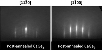
To verify that the 1 × 3 reconstruction is indeed the pattern for CaGe2, we synthesized CaGe2 using the established method of Ca deposition on Ge(111) followed by postannealing. Reference Vogg, Miesner, Brandt, Stutzmann and Abstreiter9 Starting with the annealed Ge(111) surface and growing a buffer layer of Ge, we then deposit 20 nm Ca at room temperature. During Ca growth, the RHEED pattern quickly loses its streaks and becomes featureless, indicating an amorphous Ca layer. We then proceed to heat up the sample to 750 °C to anneal and evaporate extra Ca from the surface. As the sample temperature rises, the amorphous RHEED begins to show integer order diffraction peaks of the Ge(111) lattice around 480 °C. As the temperature continues rising, the 1 × 3 reconstruction peaks appear at around 690 °C and remain for the duration of the annealing process. The final RHEED pattern for postannealed CaGe2 is shown in Fig. 3. We can see that both directions show the similar 1 × 3 reconstructed RHEED patterns as our co-deposition growth, so we verify that our co-deposition growth produces CaGe2 films. Another important conclusion is that the RHEED pattern for the co-deposition growth is significantly better than for the postannealing growth evident from the latter showing slight polycrystalline rings in the pattern. This might be due to the formation of other stable phases such as CaGe in the postannealing method, which are suppressed in the adsorption-limited growth regime.
RHEED patterns for CaGe2 prepared by depositing 10 nm Ca onto Ge(111) and postannealing up to 750 °C in UHV.

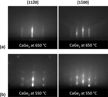
Next, we investigate the growth temperature window by performing co-deposition growth at substrate temperatures of 650 and 550 °C. Figure 4(a) shows the RHEED patterns for 650 °C, while Fig. 4(b) shows RHEED patterns for 550 °C. It is clear that as the growth temperature is decreased, the resulting CaGe2 film degrades in quality, as seen from the RHEED pattern losing the 1 × 3 reconstruction and the integer order streaks starting to exhibit superimposed dots. The dot pattern is indicative of a 3D reciprocal lattice, which emerges as the surface becomes slightly rougher and the RHEED beam diffracts via transmission through islands on the surface. The asymmetry of the dot pattern is due to a slight out-of-plane tilt of the sample holder.
(a) RHEED patterns for co-deposited CaGe2 grown at 650 °C. (b) RHEED patterns for co-deposited CaGe2 grown at 550 °C.

We next focus on the conversion of the CaGe2 films to germanane by submerging in 37% HCl solution (aqueous) at various temperatures (−40 °C to room temperature) and for various times (1–24 h). Reference Bianco, Butler, Jiang, Restrepo, Windl and Goldberger5,Reference Vogg, Brandt and Stutzmann11 For characterization by x-ray diffraction and Raman spectroscopy, we synthesize a 150 nm CaGe2 film (sample A) and de-intercalate by submerging in HCl at 5 °C for 1 h. The θ–2θ x-ray diffraction scan for the resulting film shows two peaks [Fig. 5(b)]. The peak at 2θ = 27.3° is from the Ge(111) substrate [see Fig. 5(a)], while the peak at 2θ = 15.2° corresponds to the (0001)-oriented germanane. Reference Bianco, Butler, Jiang, Restrepo, Windl and Goldberger5 This confirms that the resulting film is germanane. The inset of Fig. 5(b) shows a RHEED pattern taken with beam energy of 30 kV. The diffraction spots form a circular pattern and slide with azimuthal rotation, which indicates a 2D reciprocal lattice. The single RHEED pattern also indicates that the orientation of the germanane film is determined by the underlying Ge(111) substrate. Raman spectroscopy also indicates that the resulting film is germanane. Figure 5(c) shows the Raman spectrum for sample A (orange curve), which is different from the Raman spectrum of bare Ge(111) substrate (black curve) which has a single peak at 297 cm−1 Raman shift. For sample A, we observe two large peaks on the Raman spectrum. The peak at 228 cm−1 corresponds to the A1 germanane mode, while the E2 GeH mode at 302 cm−1 can be seen as a kink on the Ge(111) substrate peak. These peaks are consistent with Raman spectra of bulk germanane crystals. Reference Bianco, Butler, Jiang, Restrepo, Windl and Goldberger5 Because the A1 peak is specific to germanane (not present in bulk germanium), it is a strong indicator for the presence of germanane. Thus, x-ray diffraction, RHEED, and Raman spectroscopy provide very strong evidence that the resulting film is germanane.
(a) θ–2θ x-ray diffraction scan of a Ge(111) substrate. (b) θ–2θ x-ray diffraction scan of a 150 nm GeH film (sample A). The peak at 15.2° corresponds to (0001)-oriented GeH. Inset: RHEED pattern of sample A with beam along
 $[1\bar 100]$
and beam energy of 30 kV. (c) Raman spectra for sample A (orange curve) and Ge(111) substrate (black curve). Data are plotted on a log scale.

To investigate the morphology of the film, we perform ex situ AFM measurements on a thin 5 nm CaGe2 film (sample B) before and after de-intercalating in HCl at −40 °C for 1 h (Fig. 6). For reference, we show an AFM scan of a 5 nm Ge buffer layer on a Ge(111) substrate taken from the same wafer [Fig. 6(a)]. This Ge buffer layer is grown at 650 °C and then heated to 750 °C to reproduce the conditions just prior to the CaGe2 deposition. AFM of the Ge buffer layer shows the formation of terraces due to the miscut of the Ge(111) substrate. The typical height of each terrace is ∼5 nm. Figure 6(b) shows that with the growth of 5 nm CaGe2, the terrace size becomes larger. This indicates the propensity for the CaGe2 to grow flat on the (111) plane. To maintain the global miscut of the substrate, the terrace height also increases to typical values of ∼10 nm (note that a terrace width of a few micrometers and height of ∼10 nm corresponds to a miscut of ∼0.2°). After de-intercalation [Fig. 6(c)], the overall terrace size is similar to the CaGe2 film. To determine the local roughness of the film, we analyze the rms roughness within individual terraces. We find that the Ge buffer has rms roughness of 0.26 nm, the CaGe2 film has rms roughness of 0.40 nm, and the germanane film has rms roughness of 0.25 nm. Most importantly, even after submerging in HCl solution to obtain germanane, the individual terraces remain atomically smooth. For reference, we perform RHEED measurements on sample B after HCl processing [Fig. 6(d)]. These patterns are similar to sample A [Fig. 5(b), inset] with 2D-like diffraction spots, but are dimmer due to the 15 kV beam voltage. The 2D-like pattern is consistent with the atomic scale smoothness indicated by the AFM measurements.
(a) AFM image of Ge(111) substrate. (b) AFM image of 5 nm CaGe2 on Ge(111) (sample B). (c) AFM image of sample B after de-intercalation in HCl solution for 1 h at −40 °C (i.e., 5 nm GeH). (d) RHEED pattern of 5 nm GeH with beam along
 $[1\bar 100]$
.

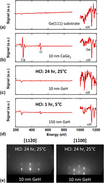
Auger electron spectroscopy is used to further characterize the films. For reference, Fig. 7(a) shows the Auger spectrum of a Ge(111) substrate prepared by chemical etching and UHV annealing to remove surface oxides as discussed earlier. This spectrum is measured in situ after the UHV annealing. Important features here are the relatively small oxygen peak at 510 eV and the presence of very weak Ge peaks in the 1000–1200 eV range. There is also a small peak near 260 eV that is likely to come from carbon contamination. Figure 7(b) shows the Auger spectrum taken after co-deposition growth of 10 nm CaGe2 (sample C), giving a clear Ca peak at 294 eV and still maintaining the Ge peaks in the 1100 eV range. This spectrum is taken ex situ and the large O peak likely appears due to exposure of CaGe2 films to atmosphere. Next, we perform de-intercalation by HCl at room temperature for 24 h and subsequently measure the Auger spectrum [Fig. 7(c)]. The Ca peak disappears from the pattern (within noise limits), while the small peak near 260 eV remains, similar to the fresh Ge(111) surface. Despite the exposure to atmosphere, the O peak is severely reduced, which indicates that the film is relatively resistant to oxidation. For comparison, we perform Auger spectroscopy on sample A after de-intercalation (150 nm thick, 5 °C, 1 h) and a very similar Auger spectrum is obtained. To compare the de-intercalation at higher temperatures and for longer times, we perform RHEED measurements on sample C and the resulting patterns are shown in Fig. 7(d). Unlike sample A (5 °C, 1 h) and sample B (−40 °C, 1 h) which exhibit 2D patterns, sample C exhibits 3D-like RHEED patterns (i.e., fixed spots that change in intensity as the sample is rotated in-plane). This indicates that germanane films are smoother for lower temperatures and shorter times of the HCl processing. More detailed studies are needed to better understand the de-intercalation process.
(a) In situ Auger spectrum for Ge(111) prepared by chemical etching and UHV annealing. (b) Ex situ Auger spectrum for a 10 nm CaGe2 film (sample C). (c) Auger spectrum for sample C after HCl immersion at 25 °C for 24 h. (d) Auger spectrum for sample A after HCl immersion at 5 °C for 1 h. (e) RHEED patterns for sample C after HCl immersion.

IV. CONCLUSION
We have demonstrated the successful co-deposition of CaGe2 films on Ge(111) by MBE. The growth occurs within an adsorption-limited growth regime with overpressure of Ca, which ensures stoichiometry of the film. The best RHEED patterns are obtained at a growth temperature 750 °C. We compare this new growth method with previous methods based on Ca deposition on Ge(111) and postannealing. We find that the co-deposition method produces RHEED patterns that are free of the polycrystalline rings that occur for the postannealing growth, which suggests that the co-deposition method inhibits the formation of other stable phases such as CaGe. The CaGe2 films are then immersed in hydrochloric acid and subsequent characterizations by x-ray diffraction and Raman spectroscopy indicate that the resulting film is germanane. RHEED patterns indicate that the crystalline orientation of the germanane film is determined by the underlying Ge(111) substrate. Furthermore, both RHEED and AFM measurements indicate that the local morphology is smooth at the atomic scale. However, the grain size is limited to a few micrometers, primarily due to the miscut of the Ge substrate. Thus, optimization of the substrate could yield much larger grain sizes. These results provide a significant advance toward the long-term goal of developing large area germanane.
ACKNOWLEDGMENTS
We acknowledge the technical assistance of Hua Wen and Yunqiu Kelly Luo. This work was supported by ARO (Grant No. W911NF-11-1-0182), NSF (Grant No. DMR-MRSEC 0820414), UC Labs (Grant No. 12-LR-239009), ONR (Grant No. N00014-12-1-0469), and ENCOMM. JEG acknowledges the support of ARO (Grant No. W911-NF-12-1-0481).