Introduction
Wireless power transfer (WPT) has attracted increasing attention in recent years due to its promising applications in mobile electronics, biomedical implants, industrial sensors, and electric vehicles [Reference Lu, Huang and Liu1–Reference Moeini, Horestani and Fumeaux4]. However, traditional resonant inductive coupling systems often suffer from performance degradation in the over-coupled regime, where mode (frequency) splitting occurs, and they are highly sensitive to environmental variations [Reference Yang, Yu and Kou5–Reference Lee, Yoon, Song, Hong, Oh and Nam7]. In conventional strongly coupled resonant WPT, frequency- or impedance-tuning strategies have been widely analyzed and experimentally validated using equivalent circuit models to cope with the frequency-splitting behavior in the over-coupled regime [Reference Heebl, Thomas, Penno and Grbic8–Reference Sis and Kavut10]. As a robust alternative, parity–time (PT) symmetric WPT architectures – conceptually derived from quantum mechanics [Reference Stolz and Müller11] – have been introduced to balance internal gain and loss [Reference Dai, Peng, Wang, Li, Zhou, Wang, Chen, Zhang and Wang12–Reference Sun, Yang, He, Dong, Liang, Wei, Chen and Sun14]. Since Assawaworrarit et al. first demonstrated that PT-symmetry enables stable energy delivery under strong coupling without active frequency tuning [Reference Assawaworrarit and Fan15], subsequent research has extensively focused on improving efficiency and transmission range through advanced amplifiers, coil arrays, and optimized resonant topologies [Reference Yan and Yan16–Reference Assawaworrarit, Yu and Fan19].
However, most PT-symmetric WPT systems operate at a single frequency, limiting their adaptability in scenarios with multiple device types, EMI, or dynamic resonant shifts [Reference Pham, Ha-Van, Le, Nguyen and Sekiya17, Reference Zhang, Chen and Cao20–Reference Zhang, Zhu, Guo, Chen, Sun, Jiang, Li, Yu and Chen22]. In practice, emerging applications increasingly demand systems that support multiple resonant frequencies or allow reconfiguration to meet diverse requirements [Reference Atallah, Hussein and Abdel-Rahman23–Reference Mercier and Chandrakasan25]. Conventional approaches to realize multi-frequency operation typically rely on tap-switching or segmented-coil techniques [Reference Jabbar, Rehman, Javed, Awan and Iqbal26–Reference Seo29]. While these methods can generate dual or multiple resonant modes, they usually require additional impedance matching or switching circuits and remain sensitive to coupling variation, thereby constraining robustness.
Motivated by these challenges, this work proposes a dual-frequency PT-symmetric WPT system that combines the adaptability of tap-switching with the robustness of PT symmetry. The proposed architecture provides two selectable PT operating points corresponding to two resonant modes, enabling dual-frequency operation without additional frequency-tracking control. We clarify the distinction between PT-symmetric self-oscillating gain–loss-balanced operation and conventional passive strongly coupled SP-compensated WPT, and validate the proposed design through theoretical modelling and experimental measurements demonstrating high efficiency in both modes.
System design
Theoretical analysis
In a PT-symmetric WPT system, energy is injected into the source resonator through an active gain element and subsequently transferred to the load via resonant inductive coupling [Reference Assawaworrarit, Yu and Fan19]. To achieve dual-frequency operation, the magnetic coupling component (inductor coil) can be tapped to connect with one more circuit branch, as shown in Fig. 1(a). This method can create two resonant modes for transmitter. In the proposed architecture, the transmitter incorporates two series-connected resonant branches corresponding to two distinct operating frequencies. To analyze the mode-dependent dynamics of the system, we introduce a binary frequency state variable σ ∈ {0,1}, where σ = 0 and σ = 1 denote the low- and high-frequency modes, respectively. And the switching index σ represents the tapped-coil configuration, which changes the effective inductance. Besides, according to the framework of magnetic coupling resonance theory and to simplify the subsequent analysis, it is typically assumed that the transmitter and receiver share an identical self-resonant frequency. Under this condition, we employ a coupled-mode theory (CMT) formulation as a reduced-order approximation of the underlying compensated circuit model to capture the dominant near-resonant modal interaction and the gain–loss balance in the PT-symmetric WPT link [Reference Assawaworrarit and Fan15]. The CMT model assumes near-resonant operation and slowly varying envelopes of the fundamental resonant modes; therefore, it does not explicitly account for switching harmonics, strong nonlinearities (e.g., device saturation), or distributed parasitics that may become relevant at higher power or far-from-resonance operation. With these assumptions, the mode-dependent dynamics of the coupled system can be expressed as follows:
 \begin{equation}\frac{{\text{d}}}{{\,{\text{d}}t}}\left[ {\begin{array}{*{20}{l}}
{{a_s}} \\
{{a_r}}
\end{array}} \right] = \left[ {\begin{array}{*{20}{c}}
{i{\omega _1}(\sigma ) - {g_n}}&{ - ik(\sigma )} \\
{ - ik(\sigma )}&{i{\omega _2}(\sigma ) + \varphi }
\end{array}} \right]\left[ {\begin{array}{*{20}{l}}
{{a_s}} \\
{{a_r}}
\end{array}} \right].\end{equation}
where k(σ) denotes the coupling coefficient under the selected frequency mode which can be given by
 \begin{equation}k(\sigma ) = \left\{ {\begin{array}{*{20}{l}}
{{k_L},}&{{\text{ if }}\sigma = 0{\text{ (low - frequency mode) }}} \\
{{k_H},}&{{\text{ if }}\sigma = 1{\text{ (high - frequency mode). }}}
\end{array}} \right.\end{equation}
Schematic diagram of a switch-mode PT symmetric wireless power transfer circuit with dual-frequency switchability: (a) system configuration and (b) its equivalent circuit diagram.

The corresponding modal amplitudes are represented by a s and a r, respectively. The net gain rate is expressed as g n = g − φ s, where g denotes the overall gain provided by the negative resistance R N, and φ s accounts for the inherent loss arising from the resistance of the transmitting coil. The total loss within the system is defined as φ = φ L + φ r, comprising both the load-induced dissipation φ L and the intrinsic ohmic loss of the receiving coil φ r. Assuming the resonator amplitudes evolve proportionally as eiω(σ)t. Besides, ω 1(σ) and ω 2(σ) denote the intrinsic (uncoupled) resonant angular frequencies of the source (Tx) and receiver (Rx) resonators under the switching state  $\sigma $, respectively. To derive the characteristic equation, we assume the resonator amplitudes evolve proportionally as a s(t) = A s eiω(σ)t, a r(t) = A r eiω(σ)t, where ω(σ) is the steady-state oscillation angular frequency of the coupled system. Substituting these expressions into Eq. (1) and canceling the common factor eiω(σ)t yields the following algebraic equations:
 \begin{equation}\begin{array}{*{20}{l}}
{\left[ {i\left( {\omega (\sigma ) - {\omega _1}(\sigma )} \right) - {g_n}} \right]{A_s} + ik(\sigma ){A_r} = 0} \\
{ik(\sigma ){A_s} + \left[ {i\left( {\omega (\sigma ) - {\omega _2}(\sigma )} \right) + \varphi } \right]{A_r} = 0}.
\end{array}\end{equation}
These equations can be written in matrix form as
 \begin{align}\left[ {\begin{array}{*{20}{c}}
{i\left( {\omega (\sigma ) \!-\! {\omega _1}(\sigma )} \right) \!-\! {g_n}}&{ik(\sigma )} \\
{ik(\sigma )}&{i\left( {\omega (\sigma ) \!-\! {\omega _2}(\sigma )} \right) \!+\! \varphi }
\end{array}} \right] \nonumber \\
\left[ {\begin{array}{*{20}{l}}
{{A_s}} \\
{{A_r}}
\end{array}} \right] \!= \!\left[ {\begin{array}{*{20}{l}}
0 \\
0
\end{array}} \right] .\end{align}
A non-trivial solution (A s, A r) ≠ (0, 0) exists only if the determinant of the coefficient matrix equals zero. Therefore, the characteristic equation is obtained as
 \begin{equation}\left( {\omega (\sigma ) - {\omega _1}(\sigma ) + i{g_n}} \right)\left( {\omega (\sigma ) - {\omega _2}(\sigma ) - i\varphi } \right) - k{(\sigma )^2} = 0.\end{equation}
To determine the eigenfrequencies of the system, we solve the characteristic Eq. (5) and obtain
 \begin{equation}\left( {\omega (\sigma ) - {\omega _1}(\sigma )} \right)\left( {\omega (\sigma ) - {\omega _2}(\sigma )} \right) + {g_n}\varphi - k{(\sigma )^2} = 0.\end{equation}
 \begin{equation}\qquad\qquad\,\,\,\,\varphi \left( {\omega (\sigma ) - {\omega _1}(\sigma )} \right) - {g_n}\left( {\omega (\sigma ) - {\omega _2}(\sigma )} \right) = 0.\end{equation}
From Eqs. (6) and (7), set the real and imaginary parts to zero, respectively, and assuming that ω 2(σ) = ω 1(σ) = ω 0(σ), where ω 0(σ) denotes the common uncoupled resonant angular frequency of the Tx/Rx resonators under the switching state σ, thus we can calculate the eigenfrequency ω(σ) as
 \begin{equation}\omega (\sigma ) = \left\{ {\begin{array}{*{20}{l}}
{{\omega _0}(\sigma ) \pm \sqrt {{k^2}(\sigma ) - {\varphi ^2}} ,}&{{\text{ }}k(\sigma ) \geqslant \varphi }&{{\text{ }}} \\
{{\omega _0}(\sigma ),}&{{\text{ }}k(\sigma ) \lt \varphi .}&{\text{ }}
\end{array}} \right.\end{equation}
ω 0(σ) can be expressed as
 \begin{equation}{\omega _0}(\sigma ) = (1 - \sigma ){\omega _L} + \sigma {\omega _H}.\end{equation}
The Eq. (8) reveals two distinct dynamic regimes depending on the relative magnitude of k(σ) and the total system loss φ.
In the strong coupling regime in which k(σ) > φ, the square root term in Eq. (8) is real, and the system supports two distinct real eigenfrequencies symmetrically split around ω 0(σ). This corresponds to the unbroken PT-symmetric phase, in which the system sustains stable oscillation at either of the two eigenmodes with balanced energy exchange between gain and loss. The frequency splitting also increases with stronger coupling, reflecting enhanced mode hybridization.
In contrast, in the weak coupling regime where k(σ) < φ, the square root becomes imaginary, resulting in a pair of complex conjugate eigenfrequencies. This indicates the system is in the broken PT-symmetric phase, where the modal amplitudes become exponentially growing or decaying, and the system effectively operates at a single dominant resonance near ω 0(σ).
By inserting the respective frequency solutions corresponding to these two regimes into the coupled dynamic equations, one can extract distinct transmission behaviors that signify the system’s symmetry state.
Following the coupled-mode power-balance formulation in Assawaworrarit and Fan (Nature Electronics, 2020), the load is modelled as an additional dissipative channel of the receiver resonator characterized by the load-induced loss rate φ L. With the same CMT energy normalization, the time-averaged power extracted by a dissipative channel is proportional to the corresponding loss rate and the steady-state energy stored in that resonator mode (see Supplementary Eqs. (S1.6)–(S1.7) in [Reference Assawaworrarit and Fan15]). Therefore, the delivered load power P load can be written in the closed form given in Eq. (10). For each receiver resonator, the power delivered P load and the transmission efficiency η can be written as
 \begin{equation}{P_{{\text{load }}}} = {\omega _0}(\sigma )\varphi {\left| {{a_s}} \right|^2} = \left\{ {\begin{array}{*{20}{l}}
{\frac{{{\omega _0}(\sigma )k{{(\sigma )}^2}}}{\varphi }{{\left| {{a_s}} \right|}^2},}&{k(\sigma ) \lt \varphi } \\
{{\omega _0}(\sigma )\varphi {{\left| {{a_s}} \right|}^2},}&{k(\sigma ) \geqslant \varphi }.
\end{array}} \right.\end{equation}
 \begin{equation}\eta = \frac{{{\varphi _l}|{a_r}{|^2}}}{{{\varphi _s}|{a_s}{|^2} + ({\varphi _r} + {\varphi _l})|{a_r}{|^2}}} = \left\{ {\begin{array}{*{20}{c}}
{\frac{{1 - \frac{{{\varphi _r}}}{{{\varphi _r} + {\varphi _l}}}}}{{1 + \frac{{{\varphi _s}}}{{{\varphi _r} + {\varphi _l}}}}},\quad k(\sigma ) \geqslant \varphi } \\
{\frac{{1 - \frac{{{\varphi _r}}}{{{\varphi _r} + {\varphi _l}}}}}{{1 + \frac{{{\varphi _s}({\varphi _r} + {\varphi _l})}}{{k{{(\sigma )}^2}}}}},\quad k(\sigma ) \lt \varphi }.
\end{array}} \right.\end{equation}
The transfer efficiency is defined as η = P load/P in. Following the power-balance derivation in the Supplementary Information of [Reference Assawaworrarit and Fan15], the injected power is distributed among the intrinsic loss of the Tx resonator, the intrinsic loss of the Rx resonator, and the load dissipation (modelled by φ L). With the same CMT energy normalization, substituting the steady-state modal amplitudes of the coupled system into this power-balance relation yields the analytical efficiency expression reported in Eq. (11).
From Eqs. 10 and 11, it can be observed that when k ≥ φ, the power delivered to the load and the transmission efficiency of the system both become independent of the coupling coefficient. Besides, when k < φ, the transmission efficiency is primarily determined by the intrinsic loss at the source side φ s and the total loss at the receiver side φ. Moreover, since φ s ≪ φ, the system is capable of sustaining highly efficient energy transfer.
Architecture
As shown in Fig. 1(a), the negative-resistance source is realized by an N-channel MOSFET (IRF840, TO-220 package) operated in the switch-mode. The IRF840 is chosen for its high breakdown voltage (500 V) and adequate switching speed (turn-on delay 25–60 ns, rise time 75–160 ns), which are sufficient for the 400–800 kHz operating range. To generate the gate signal, a 5 V sinusoidal waveform from a function generator is first converted into a square waveform using a high-speed comparator (LT1711, Analog Devices). This square wave is then buffered by a gate driver (LM5114, Texas Instruments), which provides large source/sink current capability to rapidly charge and discharge the input capacitance (C iss ≈ 1300 pF) of the IRF840, thereby ensuring sharp switching transitions. The amplifier is powered by a regulated 8 V DC supply, corresponding to a maximum experimental input power of approximately 2 W. Once oscillation is initiated, the circuit maintains self-sustained operation without external feedback control, leveraging the intrinsic nonlinear behavior of the MOSFET stage to satisfy the PT-symmetry condition.
To ensure efficient power delivery, the impedance matching network of the proposed system is realized by the series–parallel (SP) resonant topology shown in Fig. 1(b). Specifically, the capacitor C0 is connected in shunt with the switching transistor to provide voltage shaping and soft switching conditions, while the series branch composed of CT and the transmitting coil inductance L T(σ) compensates the equivalent input reactance at both resonant modes (i.e., L T(σ = 1) = L T1 and L T(σ = 2) = L T2). In this way, the effective input resistance seen from the MOSFET drain is maintained close to zero at resonance, thereby satisfying the PT-symmetric condition while simultaneously maximizing power transfer. Additionally, the load is modeled as an equivalent resistance R, which represents the reflected impedance of the receiving coil together with its rectified load.
In addition, the parameters of other components in the circuit are shown in Table 1. In the proposed system, to enable dual-frequency operation within a compact and efficient WPT architecture, a tapped transmitting coil was developed using a single-layer planar winding structure. The coil is fabricated with 0.05 mm × 1000-strand Litz wire to reduce AC resistance and minimize skin and proximity losses, ensuring high Q-factor performance. As illustrated in Fig. 2, a total of 16 turns is wound on a planar frame. A tapped point is introduced at the 10th turn (counted from the inner end), at this tapping location, the enamel insulation is locally removed by chemical stripping combined with thermal treatment, ensuring that the copper strands are cleanly exposed without mechanical damage. The exposed strands are then consolidated and soldered using medium-temperature solder paste with a controlled hot-air process, followed by precision reinforcement with a soldering iron to provide mechanical stability. To minimize parasitic effects, the tapping lead is kept as short as possible and aligned with the winding plane, which reduces additional inductance and contact resistance. This fabrication approach yields a stable low-resistance connection while preserving the high-Q characteristics of the transmitting coil.
Model of the transmitting coil.

Parameters of the circuit

The coil is thus divided into two effective segments: one is from the tapping point to the outermost turn which corresponds to L T1, and the other is from the innermost turn to the outermost turn, corresponding to L T2. To enable dynamic frequency reconfigurability, the transmitter incorporates a switch, which is used to select between these two resonance modes. When the switch enables the full coil path, the system operates in low-frequency mode; otherwise, it operates using only the outer segment for high-frequency mode. This tapped structure avoids the need for two separate coils or bulky relay switching, effectively reducing PCB area, parasitic couplings, and circuit complexity.
Experimental setup and results
Experimental setup
To ensure proper resonance and PT symmetry in both modes, two receiver branches are designed, each equipped with a resonant coil as shown in Fig. 3(b) and a set of matching components, including a compensation capacitor and resistor, selected to align the resonant frequency and balance the overall loss.
The detailed geometric and electrical parameters of the transmitting and receiving coils are summarized in Table 2.
Structure of Tx and Rx coils: (a) Tx coil and (b) Rx coils.

The detailed geometric and parameters of the transmitting and receiving coils

Figure 4 shows the experimental setup of the proposed WPT system. A DC power supply is used to power the comparator, gate driver, and MOSFET-based switching units, while a function generator is employed to provide an initial excitation signal to assist the startup of the self-oscillating circuit. The oscilloscope is used to monitor the voltage waveforms at both the transmitter and receiver ends.
Experimental implementation of the proposed dual-frequency PT-symmetric WPT system.

Measurement procedure
Based on the dual-frequency architecture, two operating modes are tested under low-frequency and high-frequency conditions. For this first prototype, the delivered power is intentionally kept at a modest level for experimental safety and reliable proof-of-concept validation, because the switch-mode negative-resistance stage together with the resonant network may generate relatively high RF voltage/current stress during self-oscillation. The voltage waveforms at both the transmitter and receiver ends are monitored and recorded to evaluate the system efficiency and delivered load power. To ensure reproducibility, the delivered load power and end-to-end efficiency are evaluated from directly measured RMS/DC quantities after the circuit reaches steady state at each transfer distance. The DC input power is obtained from the laboratory DC power supply as P in = V DC I DC, where V DC and I DC are directly read from the DC supply display. On the receiver side, the steady-state RMS voltage V RMS is measured by the oscilloscope across the receiver LC branch (i.e., the voltage across the parallel resonant tank). The delivered load power is calculated as P load = V 2rms/R load and the end-to-end efficiency is computed as η = P load/P in. Here, R load denotes the effective load resistance under steady-state operation. In practice, it is obtained by combining the physical load resistor with the non-ideal receiver LC branch at the peak of the parallel-resonance curve (accounting for parasitics such as coil AC resistance and capacitor ESR). All RMS values are recorded after the output waveform becomes periodic and the operating frequency is stabilized for each distance.
Measurement results
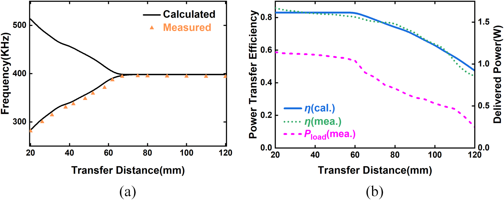
Figure 5(a) shows the calculated and measured eigenfrequencies of low-frequency operating WPT system, which indicates that the operating frequency split into two distinct branches ranging from approximately 280 to 510 kHz when the transmission distance D 1 between Tx and Rx1 is less than 65 mm indicating strong coupling region. As D 1 increases, the operational frequency converges to 398 kHz, presenting a transition into the weak coupling region. The corresponding system efficiency η and delivered power P load are depicted in Fig. 5(b), illustrating that the measured η remains above 80% in the strongly coupled region, and gradually decreases as D 1 increases. The measured delivered power at the load maintains approximately 1.0 W when D 1 ≤ 60 mm and drops to 0.2 W as D 1 equals to 120 mm.
System frequency and power transfer characteristics under low-frequency mode: (a) eigenfrequency vs. transfer distance; (b) efficiency and delivered power vs. distance.

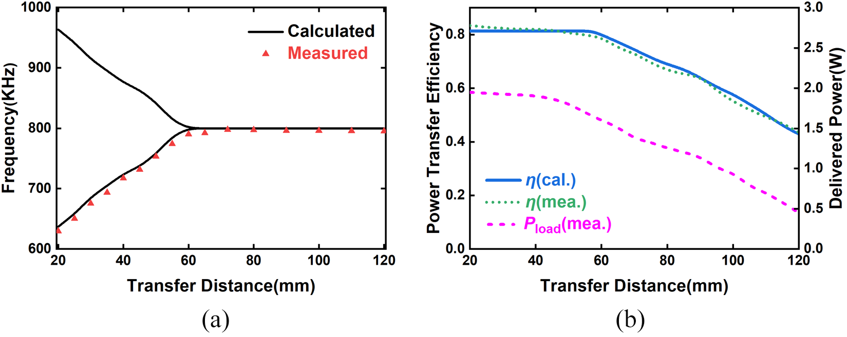
For the high-frequency mode of proposed WPT system, the operational frequency, system efficiency and delivered power level are shown in Figs. 6(a)–(b). It shows a wider frequency split range from 630 to 960 kHz than that under the low-frequency mode when the transmission distance D 2 ≤ 60 mm., after which the system enters the weak coupling region. The measured frequency aligns well with the lower branch of calculated one, which stabilizes at 801 kHz beyond the bifurcation point. Figure 6(b) illustrates that the measured system efficiency remains above 80% within 60 mm, and decreases as D 2 gets longer. The delivered power at strong coupling area can reach 1.95 W and maintains values above 1.0 W when D 2 = 95 mm. Even at 100 mm, the power remains at about 0.9 W.
System frequency and power transfer characteristics under high-frequency mode: (a) eigenfrequency vs. transfer distance; (b) efficiency and delivered power vs. distance.

From analyses above, the strong coupling region in the high-frequency mode is approximately 5 mm shorter than that in the low-frequency mode, due to the more rapid spatial decay of the electromagnetic field at higher frequencies. However, the delivered power is nearly doubled compared to the low-frequency case. This enhancement can be attributed to higher voltage swing and improved power conversion efficiency of the switching amplifier under high-frequency. Moreover, the receiver branch designed for the high-frequency mode may exhibit better impedance matching, enabling more efficient power absorption. These results highlight the dual-frequency WPT system’s ability to adaptively optimize power delivery across different operating modes.
Comparison and discussion
Such a dual-frequency switching mechanism enhances the system’s versatility and makes it more suitable for application scenarios requiring adaptive power delivery under varying frequencies or load conditions.
In comparison with prior studies in Table 3, conventional tapped-coil WPT systems [Reference Hu, He, Liu, Ng and Lee30] and dual-band designs using reactance-steering networks with reconfigurable receivers [Reference Liu and Chen31] demonstrate multi-frequency operation but suffer from efficiency degradation and strong dependence on coupling, with reported efficiencies often falling below 75%. On the other hand, PT-symmetric WPT schemes [Reference Qu, Zhang, Gu, Li and Shu32] maintain robust efficiency under varying distances but are limited to single-frequency operation. By combining both advantages, the proposed PT-symmetric dual-frequency architecture achieves stable efficiency above 80% in both operating modes, offering both frequency flexibility and coupling robustness. This dual contribution positions the system as a promising candidate for future adaptive and reliable WPT applications.
Performance Comparison

In addition to these performance advantages, practical deployment also requires considerations on power scaling and loading conditions. For this first prototype, the delivered power was intentionally kept at a modest level for experimental safety and reliable proof-of-concept validation, because the switch-mode negative-resistance stage and resonant network may produce high RF voltage/current stress during self-oscillation. For higher-power applications, scaling the delivered power requires co-optimization of the resonant link and the power stage, e.g., improving the coupling/coil quality factor (higher k and Q) and selecting low-loss switching devices and passive components with sufficient voltage/current and thermal margins, while maintaining oscillator stability and EMI compliance.
Another practical consideration is multi-receiver operation. In multi-receiver scenarios, the transmitter generally sees an effective load that depends on the number of receivers and their operating states due to the reflected impedance from each receiver. As a result, the effective load-induced loss (e.g., an equivalent φL term in the coupled-mode formulation) is no longer constant and may vary with receiver connection/disconnection and load changes. Such variations can shift the steady operating point and consequently affect the PT gain–loss balance condition as well as the coupling threshold separating different operating regimes (e.g., the onset of frequency splitting). Therefore, although the proposed dual-frequency architecture (tapped-coil switching at the transmitter together with receiver matching networks) provides a convenient front-end that may be extendable to multi-receiver applications, a complete multi-receiver model and its validation are beyond the scope of this work and will be investigated in future studies.
Conclusion
In this work, we investigate a dual-frequency switchable WPT system based on PT symmetry. Both theoretical analysis and experimental results verify that the proposed system maintains efficient and robust power transfer at two resonant operating frequencies. By controlling the on/off states of two LC resonant branches, the transmitter can switch between two distinct operating modes while preserving the PT-symmetric steady state. The proposed architecture provides a practical reference for reconfigurable dual-frequency WPT operation under varying coupling conditions. Future work will consider power scaling and extension to more complex loading conditions (e.g., multi-receiver operation) with dedicated modelling and validation.
Acknowledgment
This work was supported in part by the National Natural Science Foundation of China under Grant (62261007, 62361008) and in part by the Guizhou Provincial Basic Research Program (Natural Science) under Grant QKHJC MS [2025] 594.
Competing interests
The authors declare that they have no known competing financial interests or personal relationships that could have appeared to influence the work reported in this paper.

Wuji Sun received his Bachelor of Science degree in Electronic Information Engineering from Ludong University in 2022. Currently, he is pursuing his Master’s degree at the Ministry of Education’s Engineering Research Center for Power Semiconductor Device Reliability, School of Big Data and Information Engineering, Guizhou University. His main research area is wireless power transmission.

Shixing Yu received a bachelor’s degree in Electronic Information Engineering from the School of Electronic Engineering, Xidian University, China in 2012. He obtained a Ph.D. degree in Electromagnetic Fields and Microwave Technology from the same school at Xidian University, China in 2017. Currently, he holds the position of Associate Professor at the College of Big Data and Information Engineering, Guizhou University, China. He has authored more than 30 research articles and his current research interests include antenna and array, electromagnetic field theory, artificial electromagnetic structures, microwave devices, radio-frequency circuits, and microwave measurement.

Na Kou received a bachelor’s degree in Electronic Information Engineering from the School of Electronic Engineering, Xidian University, China in 2013. He obtained a Ph.D. degree in Electromagnetic Fields and Microwave Technology from the same school at Xidian University, China in 2018. Currently, she holds the position of Associate Professor at the College of Big Data and Information Engineering, Guizhou University, China. She has authored more than 20 research articles and her current research interests include array antennas, conformal antennas, frequency-selective radar absorbers, wireless power transfer, and vortex electromagnetic fields.