Introduction
Satellite broadcasting [Reference Balanis1,Reference Haupt2] systems such as weather forecasting, navigation, geo-imaging, live data broadcasting etc., have an advantage of a wide area-coverage as compared to the conventional terrestrial broadcasting. However, these systems demand high gain and highly efficient antennas [Reference Carver and Mink3–Reference Werner and Ganguly6] to maintain link with the satellite. Direct broadcast satellite (DBS) [Reference Murata and Fujita4] belongs to such kind of service for broadcasting television signals, which globally uses C and Ku bands on region basis. Generally, DBS services demand antennas for reception of digital signals in the 12.2–12.7 GHz frequency range. A conventional direct broadcast satellite television (DBS-TV) receiver uses a co-axial feed horn as a receiving antenna which is usually mounted on the focal point of a reflector parabolic disk. Although the co-axial feed horn provides very high gain, its main disadvantage is bulky size and heavy weight. The bulky size and heavy weight of the receiving antenna is reduced using microstrip arrays [Reference Murata and Fujita4,Reference Chen and Wu7,Reference Mousavi, Fakharzadeh and Safavi-Naeini8]. Murata et al. [Reference Murata and Fujita4] designed and experimentally validated the working of an active planar array antenna for DBS reception. Chen et al. [Reference Chen and Wu7] proposes a four-element dual linearly polarized array of microstrip elements having two different ports. The array gives 12.5 dBi gain when excited with port 1 and 11.80 dBi gain when excited with port 2. Mousavi et al. [Reference Mousavi, Fakharzadeh and Safavi-Naeini8] designed a low-cost 1K element phased array system for mobile DBS reception. The reason behind using a microstrip antenna [Reference Islam, Islam and Faruque9–Reference Awida and Fathy24] is its compactness, less weight, low cost for fabrication, relatively less complicated matching network, and easy interface with microwave devices. Moreover, conventional design of microstrip antennas for Ku band applications [Reference Kumar and Raghavan16,Reference Vijayvergiya and Panigrahi18,Reference Awida and Fathy24,Reference Bilgic and Yegin25] suffers from low gain, since the size of the antenna becomes small, which corresponds to lower surface area, that further deteriorates the gain. In order to improve the gain of the single element, a new fractal geometry is proposed in such a manner to increase the overall surface area of the element as well as to resonate the structure at 12.51 GHz. Further improvement in gain is achieved by constructing an eight-element antenna array [Reference Jin, Chin, Che, Chang, Li and Xue26–Reference Niu, Zhang, Chen and Zhong31] using the proposed single antenna.
In [Reference Carver and Mink3], Carver et al. show the dependency of resonating frequency of a microstrip antenna with its dielectric material. Kan et al. presented a spiral patch antenna, designed with a high dielectric material, to obtain good bandwidth [Reference Kan and Waterhouse5]. Douglas et al. [Reference Werner and Ganguly6] proposed fractal-based design of antennas and arrays. The idea of fractal geometries has been further explored by them to design multiband antenna array [Reference Werner and Ganguly6]. Kumar et al. [Reference Kumar and Raghavan16] presented a Ku-band antenna which is having multi-resonating slots in the back side of its cavity and it incorporated substrate-integrated waveguide (SIW) feeding for bandwidth enhancement. Pushkar et al. [Reference Vijayvergiya and Panigrahi18] proposed a dual-band microstrip patch antenna for satellite communication, which is able to fulfill the minimum spectrum requirements in the ITU-3 region. Alam et al. [Reference Alam, Faruque, Hasan and Islam19] designed a multiband microstrip antenna using FR-4 material which can operate at C, X, Ku, and K-bands. Although the antenna can show RL of −10 dB for C, X, Ku, and K-bands, it shows very poor gain performance. In [Reference Wang, Huang and Fang23], Wang et al. show that the creation of an U-slot inside a patch helps to improve the parametric results of the antenna in terms of its gain and bandwidth. A low cost 2 × 2 antenna array for Ku-band application, using SIW technology, which provides a wide bandwidth of more than 1.2 GHz has been reported by Aiwada et al. [Reference Awida and Fathy24]. A wideband, low-profile planar array for the DBS application has been presented by Mustafa et al. [Reference Bilgic and Yegin25]. A 2 × 2 array of patch antennas for Ku-band applications with wider bandwidth has been addressed by Jin et al. [Reference Jin, Chin, Che, Chang, Busuioc and Safavi-Naeini27]. The authors used differential feed with multilayer structure to get enhanced bandwidth, although the authors used multilayered structure which makes the structure bulky and the the cross polarization value along the main-beam direction is quite high.
In this paper, a linearly polarized eight element octagonal printed array for Ku-band DBS receiver application has been proposed. Each single element of the array is a 2D spiral-shaped fractal antenna with resonating frequency of 12.51 GHz. The propose spiral-shaped fractal antenna is obtained by etching alternate right-angle triangles, which are formed by rotating nine concentric squares with respect to its base square by an integer multiple of the angle 17.11° in the counter-clockwise direction. In order to get the etching portions in terms of triangular intersections, another progressive scale factor in integer multiple of 0.20, has also been imposed on the corresponding dimensions of all those concentric squares. The proposed single element gives reasonably high gain of 9.32 dBi and a bandwidth of 280 MHz with radiation efficiency of $\eta =86.70\percnt$ . The array gives a gain of 17.67 dBi and a bandwidth of 506 MHz which ensures a 100% coverage of the entire DBS service band. Both the single element as well as array gives cross polarization of −45.50 and −43.35 dB respectively, along the direction of main beam. The lower cross polarization along the main beam is achieved without employing the most commonly used technique of defected ground structure, which in turn have the tendency of drifting of resonating frequency and lowering the gain of the structure. Moreover, minor mismatch in defected ground dimension during the fabrication may cause a huge difference between the desired and obtained results.
An equivalent lumped model of the single element, in which the antenna acts as a parallel RLC circuit and its feed line as a T/Pi network has been presented. The T/Pi network has been derived from the nodal quality factor (Q n) [Reference Ludwig and Bretchko32,Reference Pozar33] of the parallel RLC load. A circuit equivalent model of eight-element octagonal array is derived by considering the proposed lumped model of the single antenna as an element of the array, and neglecting the coupling effect. The purpose of the lumped equivalent circuit model is to reconstruct the S 11 characteristics of the antenna, which gives us information about antenna's resonating frequency and its bandwidth. Therefore, using the proposed circuit model of the single element, an eight-element array model has been constructed which can be used to predict the S 11 response of the array, before designing it using CST microwave studio. Now, depending upon the obtained return loss at the desired resonating frequency and the bandwidth predicted by the array circuit model, the eight-element array has been designed using CST microwave studio, which actually takes a very long simulation time in compared with its circuit model, and hence the circuit equivalent model is significant. The circuit model provides prior information about the resonating frequency. The model has been simulated using Cadence 6.1.7, and it ensures the required frequency of operation with satisfactory return loss. It confirms a negligible amount of reflection from the load, and hence encourages to design the structure using real-time simulation software. Finally, the array with the compact feed network using a Wilkinson power divider has been designed to reduce the overall area of the array. The fabricated single element as well as the array shows a very good agreement between the simulated and measured results.
Proposed novel fractal
This section covers the formation details of the proposed single element antenna along with its fractal length and path length of the surface current.
Fractal formation
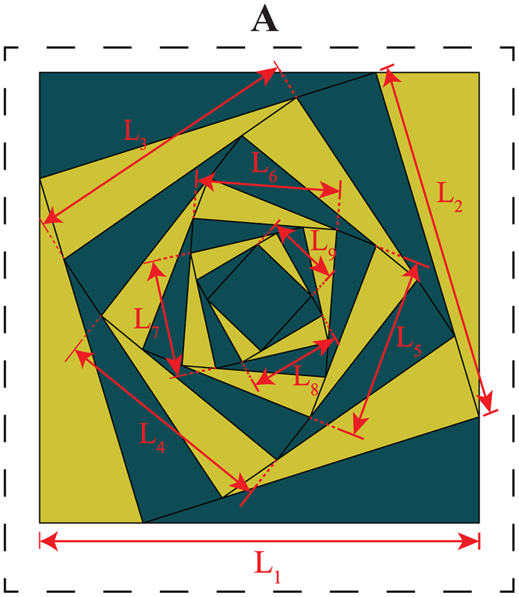
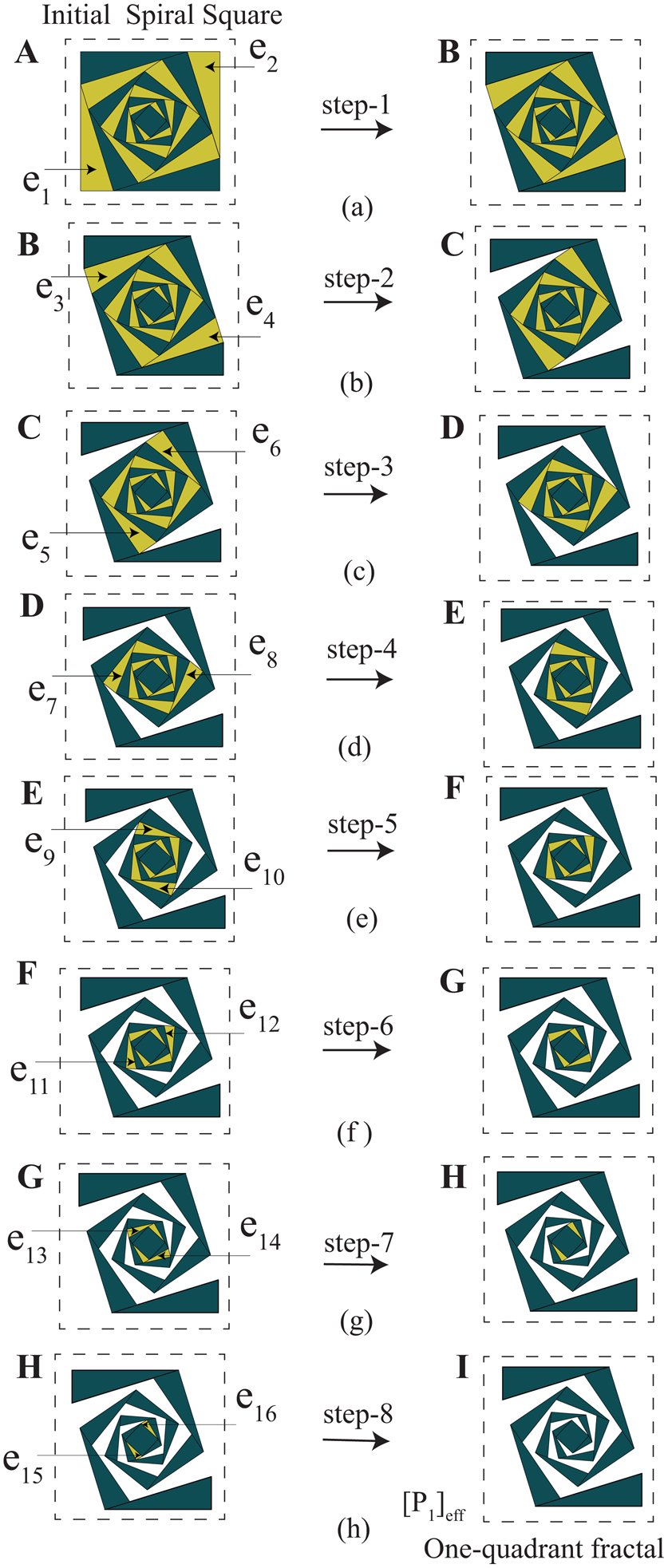
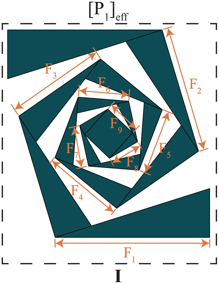
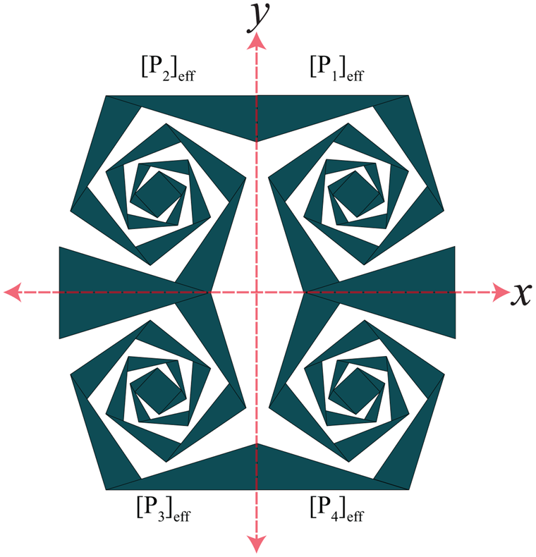
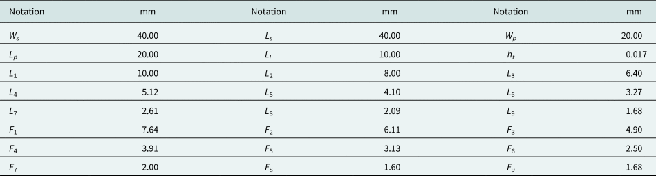
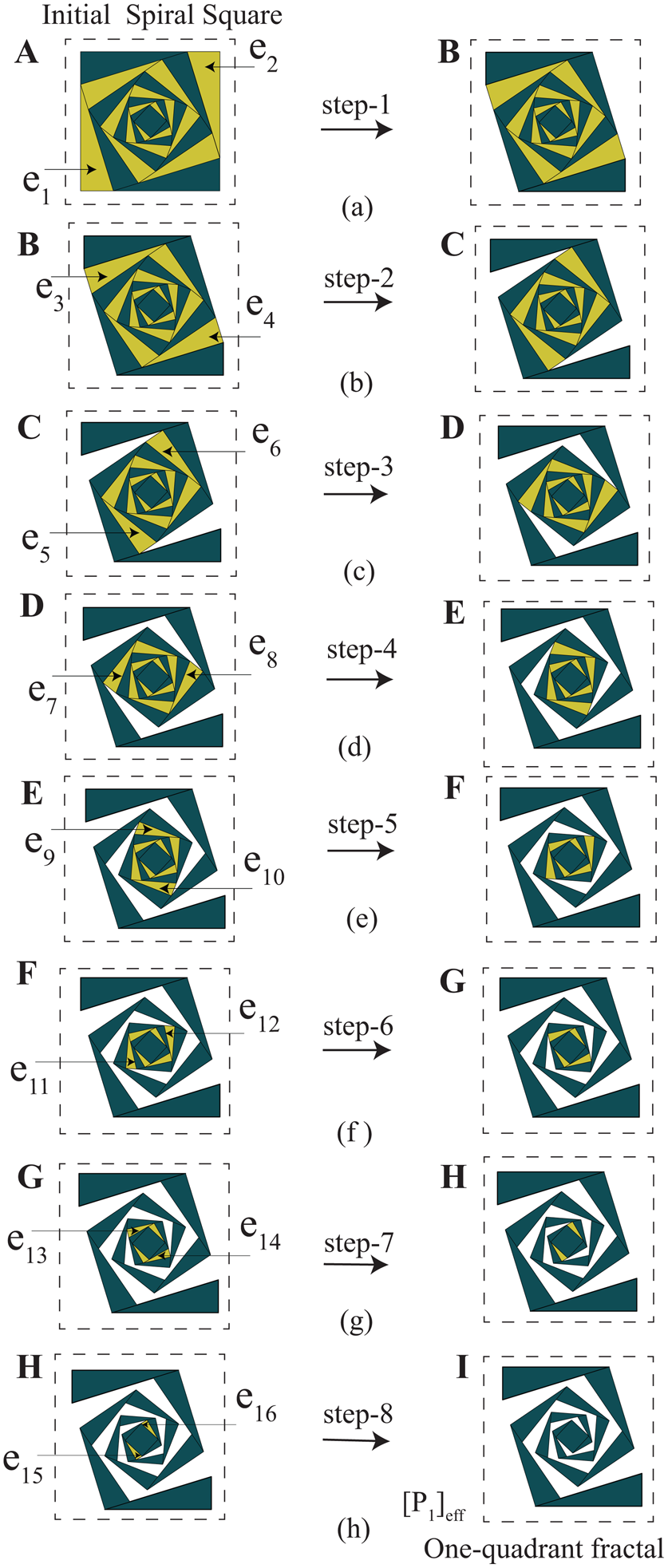
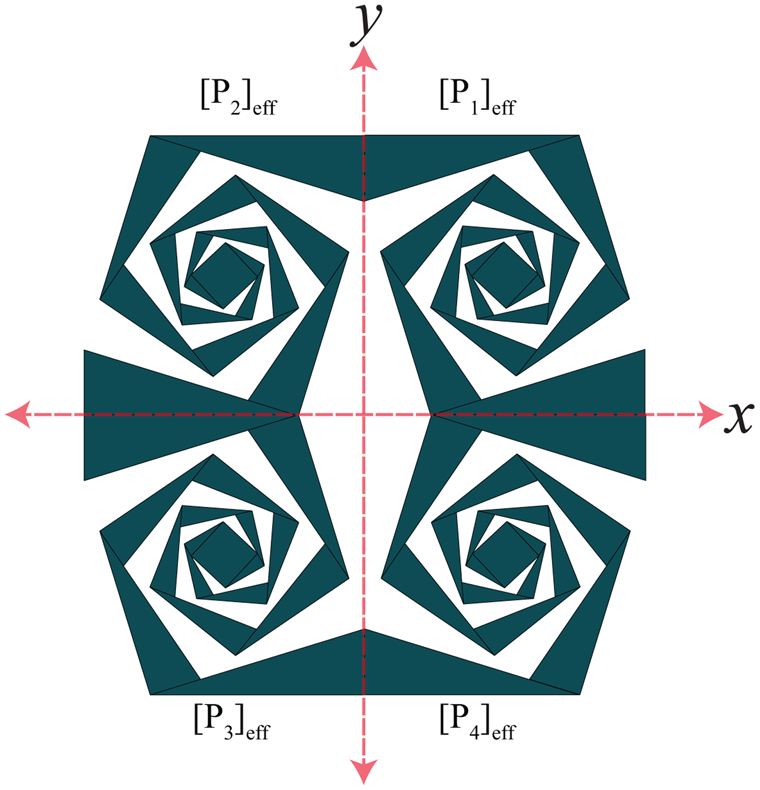
The formation of the proposed fractal geometry starts from a concentric square, which is having nine loops with a progressive scale factor of 0.20. The proposed spiral shape is obtained by rotating individual square loop by an integer multiple of 17.11° with respect to the outermost square. The resultant geometric structure, marked as A, is shown in Fig. 1 and its corresponding dimensions are listed in Table 1. The step-wise formation of one-quadrant of the required geometry is shown in Fig. 2. The outcome of step 1 is a resultant geometry marked by B, which is formed by etching the portions e 1 and e 2 from the square marked by A. The process of etching is continued up to step 8, and the portions to be etched in steps 2 to 8 are: e 3 and e 4 from B, e 5 and e 6 from C, e 7 and e 8 from D, e 9 and e 10 from E, e 11 and e 12 from F, e 13 and e 14 from G and in the endmost step, e 15 and e 16 from H. The consequences in step 2 to 8, after etching of the corresponding sections becomes: C, D, E, F, G, H, and finally I, which produces one quadrant of the proposed geometry. The dimension details of I is shown in Fig. 3. The final geometric structure is obtained by making quadrantal symmetry of Fig. 3 with respect to the axis as shown in Fig. 4.
Formation of a spiral-based fractal geometry through concentric squares.

(a)–(h) Step-wise formation of one-quadrant fractal geometry.
One-quadrant fractal geometry with dimension.

Four-fold symmetry of the proposed fractal geometry.

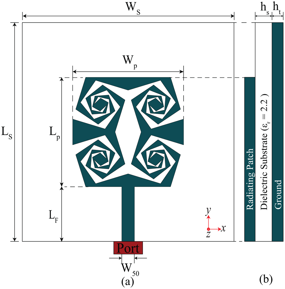
Structure and detailed dimensions of the proposed patch antenna: (a) front-view and (b) side-view.

Fractal length calculation
A fractal dimension is a statistical quantity that describes how a fractal appears to fill space. A fractal is an object that displays a property known as self-similarity, i.e. a geometric shape that can be reduced to smaller parts, with each smaller part being a reduced copy of the whole [Reference Posamentier34].
The effective fractal length of one-quadrant of the proposed geometry of Fig. 3 is obtained from equation (1):

From Fig. 4, the effective fractal length for the proposed four-fold geometry can be represented by equation (2) as:

where [P 1]eff, [P 2]eff, [P 3]eff, and [P 4]eff representthe effective length of the symmetric spiral-based fractal geometry as shown in Fig. 4.
Therefore, the total effective fractal length [P]teff of the proposed single element can be represented by equation (3) as follows:

Inserting the parameter values from Table 1 into equation (3), the fractal length of the proposed structure becomes [P] teff = 378.72 mm, which is enhanced by $118.36\percnt$ in compare to the path length of a conventional microstrip antenna having resonating frequency of 12.5 GHz.
Design of single element
Inspired from the proposed fractal geometry, a microstrip patch antenna has been designed, which is capable of operating at DBS service band and is shown in Fig. 5. The substrate material for the antenna is Rogers 5880, with thickness h s = 0.787 mm and relative permittivity of ɛr = 2.2. The thickness of all copper layers are 0.017 mm. The radiating patch is located on the top surface of the material as shown by Fig. 5. The overall area of the proposed single element is of 40 × 40 mm2. The formula relating resonating frequency with side length is presented in equation (4) [Reference Balanis1] as:

where c is the velocity of light in free space, f r is the resonant frequency of the patch antenna, ɛeff is the effective dielectric constant of the microstrip structure, and L is the side length of the patch. The detailed dimensions of the radiating patch of Fig. 5 are given in Table 1.
Current-path length calculation
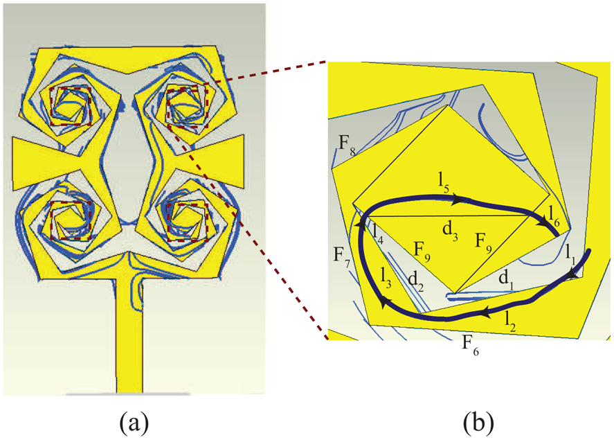
The surface current distribution is shown in Fig. 6(a). The enlarged edge path in Fig. 6(b) has been considered for the current path calculation in which the arrows represent the current direction:


where d 1 ≈ (5 × F 7)/8

where d 2 ≈ (5 × F 8)/6


where d 3 ≈ ${\lpar 3\times \sqrt {2}\times F_9\rpar }/{4}$

Hence, the computed current path length of the proposed single element is expressed as:

The calculated numeric value of L cp is almost the same as the value required to resonate the antenna at 12.5 GHz.
Current path calculation: (a) surface current of the patch antenna and (b) highlighted edge to calculate the current path length.
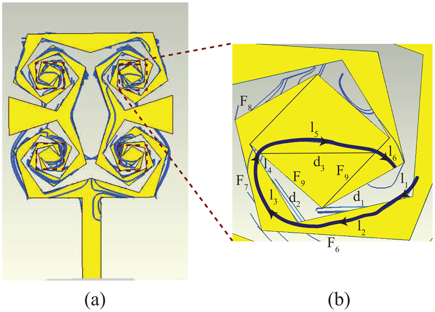
The current path length (L cp) of the proposed single element, in equations (5) to(11), is obtained from Fig. 6(b) and Table 1 respectively.
Circuit equivalent model
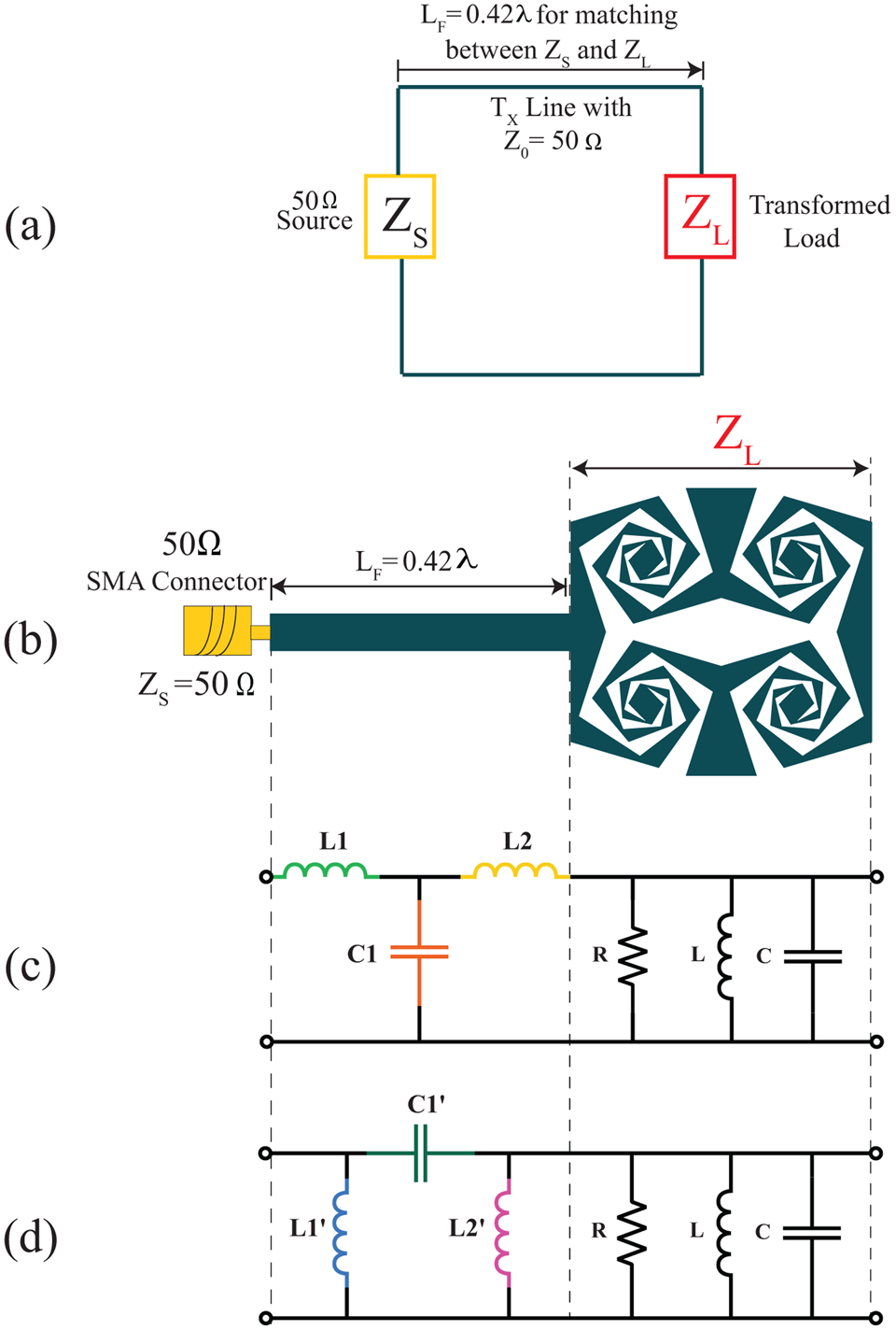
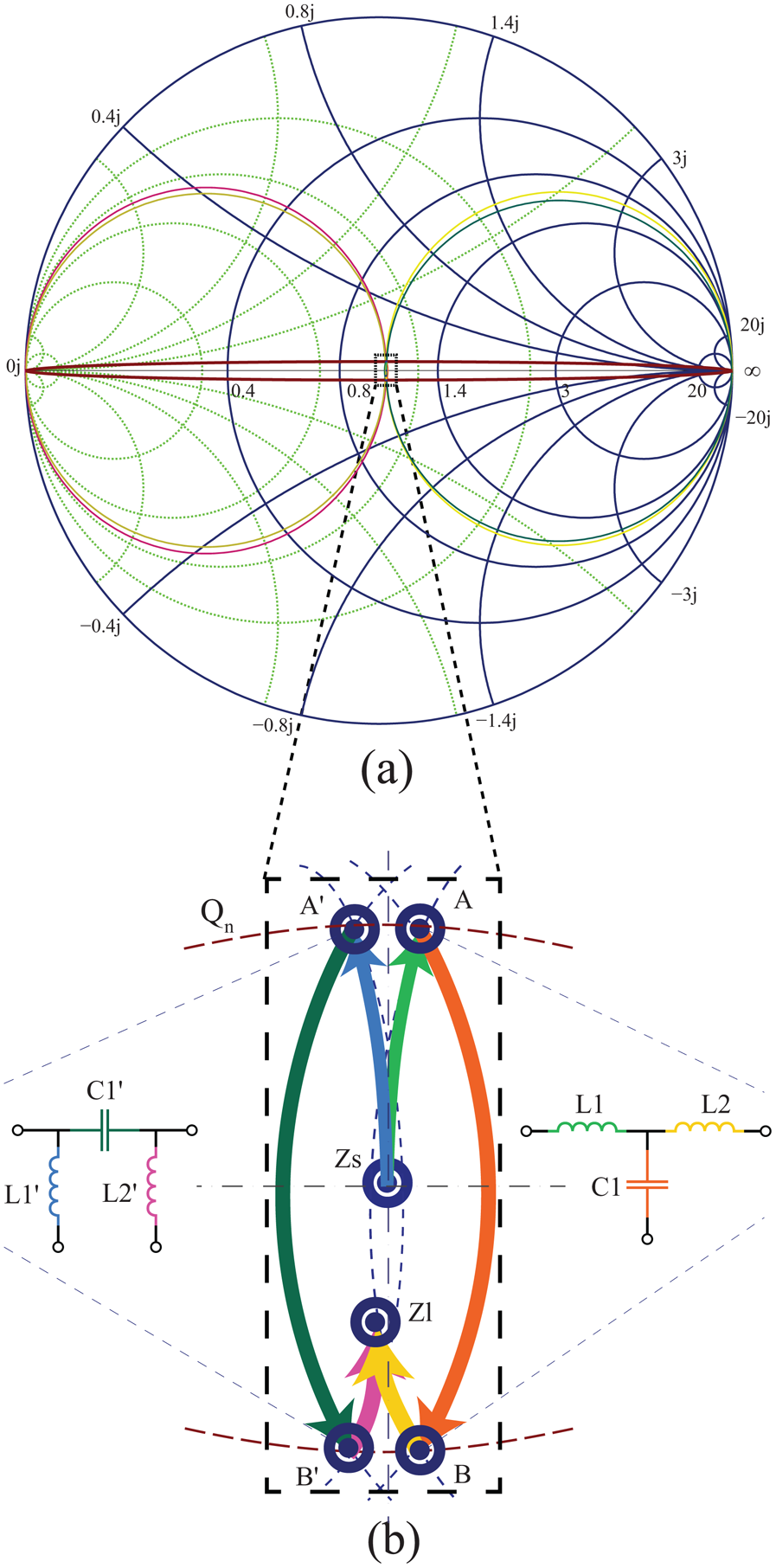
The lumped equivalent circuit model of the proposed structure is shown in Fig. 7, where the antenna modeled as a parallel RLC load. Figure 7(a) shows an impedance transformation from source to load and Fig. 7(b) represents the proposed antenna with feed. The circuit model of the proposed fractal microstrip patch antenna has been derived by source-to-load transformation, and then finding its RLC equivalent circuit. The feed line of the antenna has been modeled as a T or Pi network, by incorporating perfect matching between source and the RLC equivalent circuit by choosing proper component values of the T or Pi network. The concatenation of these two individual circuits gives the circuit equivalent model. The source impedance is considered as 50 Ω, and feed line length of the proposed antenna is 0.42λ. However, after transforming the 50 Ω source-to-load by 0.42λ, it gives the transformed impedance of the fractal geometry. Therefore, concatenation of this transformed impedance to the T/Pi equivalent model of the feed gives the complete circuit equivalent model of the proposed fractal microstrip patch antenna. Hence Figs 7(c) and 7(d) can be justified as a circuit model the proposed fractal geometry. The T/Pi network has been derived from the concept of nodal quality factor [Reference Ludwig and Bretchko32]. The purpose of introducing nodal quality in circuit design is to maintain the bandwidth requirement between the antenna and its equivalent circuit.
The proposed antenna and its lumped-equivalent model: (a) basic matching network, (b) antenna with source and feedline, (c) equivalent T-network followed by RLC load, and (d) equivalent Pi-network followed by RLC load.

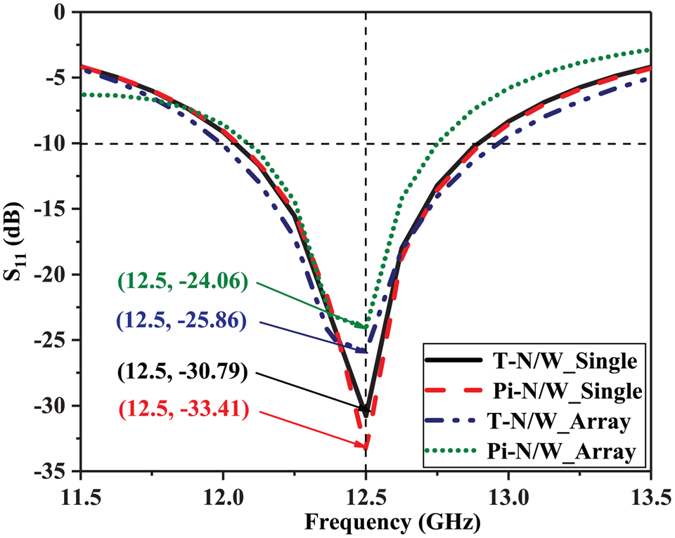
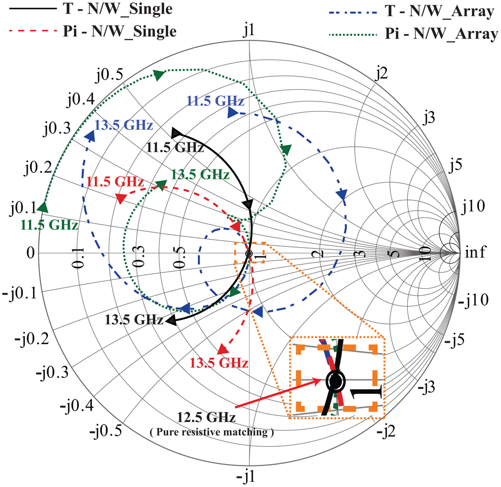
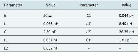
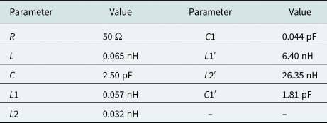
The RF signal is fed to the antenna by a 50 Ω SMA connector. Let us consider the impedance of the fractal geometry, designed using CST Microwave Studio is Z L, and the source impedance Z S is 50 Ω. In order to perform the impedance matching between Z L and Z S, a transmission line of characteristics impedance Z 0 = 50 Ω and length L F, has been implemented in-between them. The value of L F is 0.42λ, which has been obtained using the sweep parameter analysis of CST Microwave Studio. Therefore the obtained values of Z L, from Fig. 7(a), after transforming Z S by 0.42λ toward the load, becomes Z L = (1 − j0.025) Ω. The Z L has been represented by an equivalent parallel RLC [Reference Ludwig and Bretchko32] circuit, having the computed parameter values listed in Table 2. The 0.42λ long feed line, which act as a matching network between Z S and Z L, can be modeled as T/Pi RLC circuit [Reference Ludwig and Bretchko32]. Therefore, the circuit equivalent model of the single antenna becomes the concatenation of the circuit model of Z L and that of the modeled T or Pi feed line as shown in Figs 7(c) and 7(d) respectively. In order to get similarities in the S 11 graph between the circuit model and the actual antenna, the T/Pi circuit model of the matching network is derived from the Smith chart as shown in Fig. 8, by considering a nodal quality factor of Q n ≈ 0.05 [Reference Ludwig and Bretchko32] of the parallel RLC load [Reference Ludwig and Bretchko32]. The concept of Q n has been introduced to impose a similar type of bandwidth and return loss performance of the desired patch antenna to its equivalent circuit model. All the equivalent circuit models of single element as well as array presented in this paper are simulated using Cadence. The output reflection coefficients of T/Pi networks are shown in Fig. 9, which indicates an exact resonating frequency of 12.5 GHz with satisfactory bandwidth and return loss. The input impedance response of the circuits are shown in Fig. 10. The magnifying portion of Fig. 10 ensures a pure resistive input impedance of 50 Ω from the equivalent circuit at resonating frequency for both T and/or Pi type matching networks. These models reflecta similar kind of circuit characteristics of the proposed antenna and hence can be used for determining resonating frequencies, return loss, and input impedance behavior for a large array before designing it using a real-time EM simulation software.
(a) Impedance transformation using Smith chart from source to load on constant Q n contour. (b) Magnifying portion shows the transformation.

Reflection coefficient of the T and Pi Network with antenna as RLC Load.

Input impedance response of the T and Pi network with antenna as RLC Load.

Parametric value of the lumped-equivalent circuit model of single element
Design of the array
The main objective is to design an eight-element octagonal array which can operate on 12.5 GHz and gives high gain and relatively lower sidelobe level (SLL). The inter-element spacing is kept as 0.5λ [Reference Balanis1]. Octagonal geometry in the array is chosen in order to maintain a similarity with the single element, which can broadly be viewed as an octagon by considering its perimeter. The feed network of the array is designed using equal power dividers. The overall area of the octagonal array becomes 142 × 128 mm2.
Circuit equivalent model
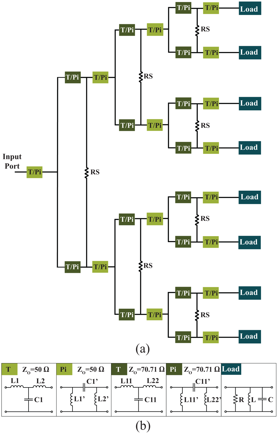
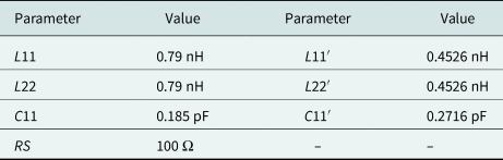
In order to get prior information about the electrical characteristics of the array, circuit equivalent models which are merely a multi-port network, shown in Fig. 11, has been derived. The proposed models show two different circuit representations of the array with feed as a Wilkinson power divider using T and/or Pi sub blocks and can replicate the electrical behavior of the array. The computed lumped parameter values are listed in Table 3. The reflection coefficient and input impedance response of the array circuit models are shown in Figs 9 and 10, respectively, which ensures about proper resonance at 12.5 GHz and perfect impedance matching at 50 Ω. The array model approximately gives bandwidth of 675 MHz. The obvious reason of getting more bandwidth in the model is the effect of fringing fields, dielectric material, ground plane, and mutual coupling effect in the actual antenna are neglected in the model and hence it predicts larger value. Inspired from these results, finally the array has been designed using CST Microwave Studio, and satisfactory results have been obtained.
(a) The circuit model of the proposed antenna array with T or Pi sub-blocks. (b) Equivalent circuit of individual blocks.

Computed lumped parameters for the circuit equivalent array model

Design of feed network
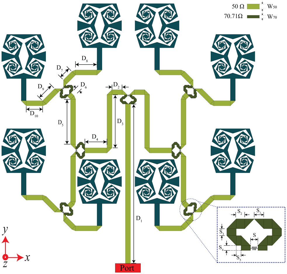
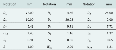
The feed network of the array has been designed in a compact manner using Wilkinson uniform power divider [Reference Wilkinson35] as shown in Fig. 12. The two different colors in Fig. 12 represent transmission lines, with characteristic impedance of 50 and 70.71 Ω and are denoted by W 50 and W 70, respectively. The corresponding dimension details in terms of length and width of the transmission lines are listed in Table 4. The magnified portion of Fig. 12 shows the detailed dimensions of the 70.71 Ω junction. A 100 Ω chip resistor (RS) is mounted on the junction at S for better isolation. It can be seen from Fig. 12 that, the proposed power divider makes the structure very compact. Moreover, at each junction of the network, since the surface current directions are opposite, the effective radiation in the horizontal direction becomes negligible which further improves the cross polarization suppression of the structure.
The structure of the array and detailed dimensions of its feed network.

Dimensions of antenna array prototype

Results and discussion
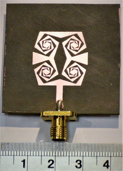
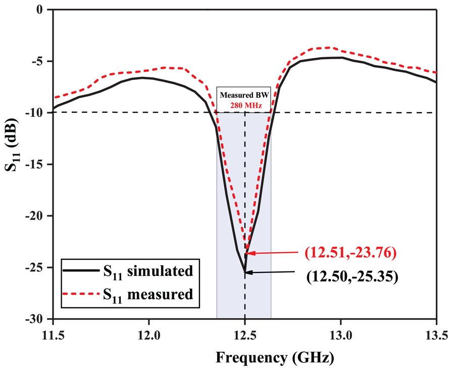
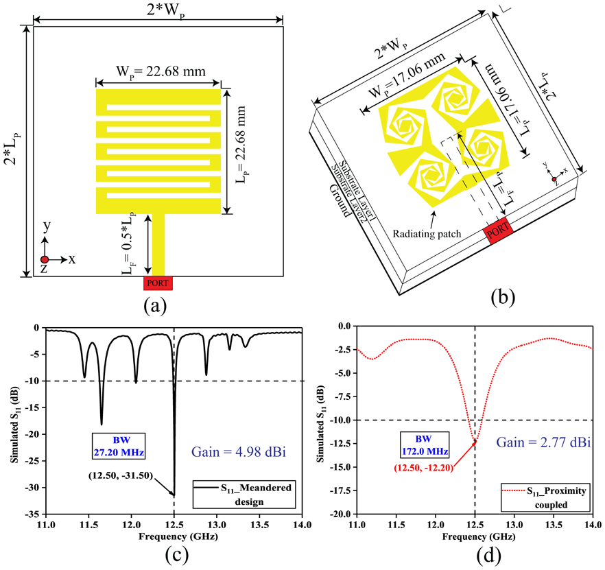
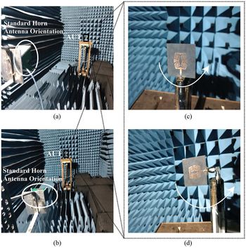
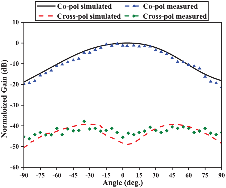
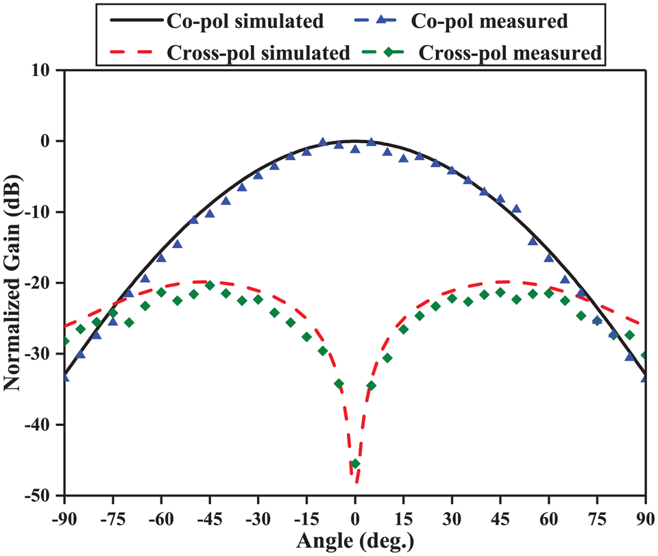
The proposed single element and the array are fabricated. The fabricated single element is shown in Fig. 13 and its return losses is shown in Fig. 14. It can be seen from Fig. 14 that the fabricated prototype resonates at 12.51 GHz and gives a return loss of −23.76 dB. The measured bandwidth, from Fig. 14, becomes 280 MHz. A comparison between the proposed single element and a Meandered structured of same resonating frequency has been carried out. The gain and the return loss of the Meandered structured, designed, and simulated using CST, is shown in Fig. 15(a). The presented fractal with proximity coupled feed is also simulated using CST and its performance is shown in Fig. 15(b). Both Figs 15(a) and 15(b) ensure that the proposed single element with microstrip feed, give much better gain and bandwidth compared with Meandered structured and same structure with proximity coupled feed. The radiation pattern of the single element and the array are measured inside an anechoic chamber. Figure 16 shows the experimental inside set-up of the anechoic chamber for E and H-plane radiation pattern measurement of the single element. The same procedure has been followed to determine the radiation characteristics of the array. The E- and H-plane radiation patterns of the single element are shown in Figs 17 and 18. Moreover, from Figs 17 and 18, it can be seen that the measured value of cross polarization along the direction of main beam is −45.50 dB, which ensures a good antenna design [Reference Balanis1]. The lower cross polarization along main beam is achieved without tampering the ground plane of the structure.
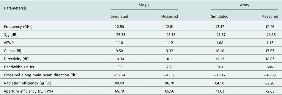
Directivity of the fabricated single element is computed as [Reference Balanis1] 10.11 dBi. The aperture efficiency (ηap) of the antenna can be calculated from equations (12) and (13) as follows [Reference Ma and Vandenbosch36,Reference Vosoogh and Kildal37]:


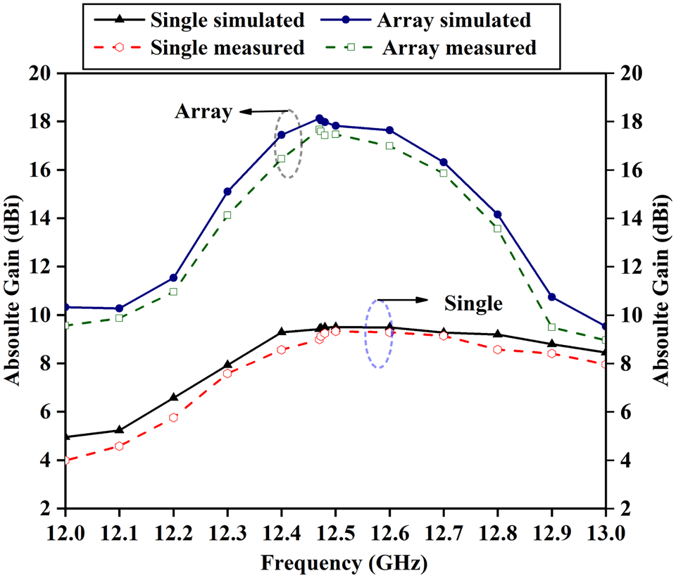
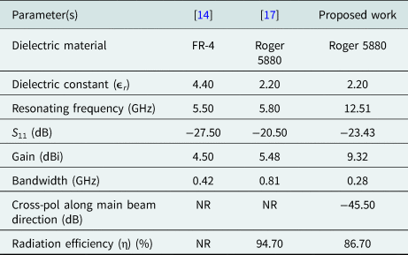
where A is the overall effective area of the patch in m2, and D is the obtained directivity of the antenna in dBi. The simulated and measured aperture efficiency (ηap) of the single element are 66.79 and 65.56% respectively. The measured gain of the fabricated single element at 12.51 GHz is obtained as 9.32 dBi. The simulated and measured gain vs. frequency graph is presented in Fig. 19. Measured voltage standing wave ratio (VSWR) of the fabricated single element is obtained as 1.12. The measured parametric results of the single element prototype are listed in Table 5. It can be observed from Table 5 that a satisfactory measured results are obtained with respect to their simulated values. A comparison of the proposed spiral-based fractal antenna with other existing non-fractal spiral design has been performed and the results are listed in Table 6. It can be observed from Table 6, that the proposed fractal gives maximum measured gain of 9.32 dBi, over the other non-fractal spiral antennas, reported in the literature.
Fabricated single element.

Reflection coefficient of the single element.

(a) Meandered structured antenna. (b) Proposed antenna with proximity-coupled feed. (c) S 11 characteristics of (a). (d) S 11 characteristics of (b).

Experimental set-up inside the anechoic chamber for the single element: (a) horn orientation for Co-pol measurement, (b) horn orientation for Cross-pol measurement, (c) H-field measurement set-up, and (d) E-field measurement set-up.

E-plane co- and -cross polarization radiation patterns of the single element.

H-plane co- and cross polarization radiation patterns of the single element.

Simulated and measured gain of single element and the array.

Parametric results of the single element and the array

Comparative performance of fabricated single element and non-fractal spiral antenna

NR, not reported.
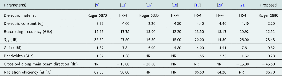
The comparative performance of the proposed single element with other microstrip antennas operating in the X and Ku bands are shown in Table 7. It can be seen from Table 7 that the proposed structure gives maximum of gain among the others operating at DBS band. Furthermore, it gives lowest cross polarization of − 45.50 dB along the main beam direction, which is far better than the others in Table 7 operating in the same band.
Comparative performance of fabricated single element

NR, not reported.
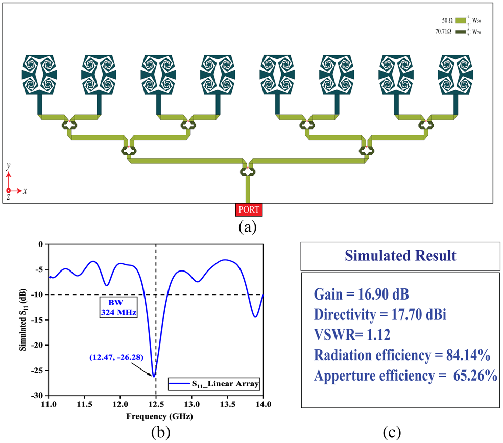
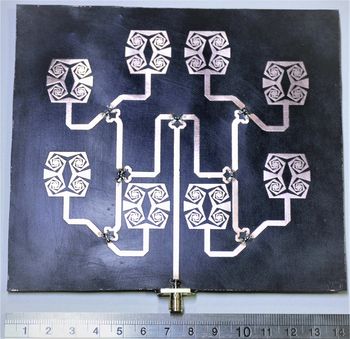
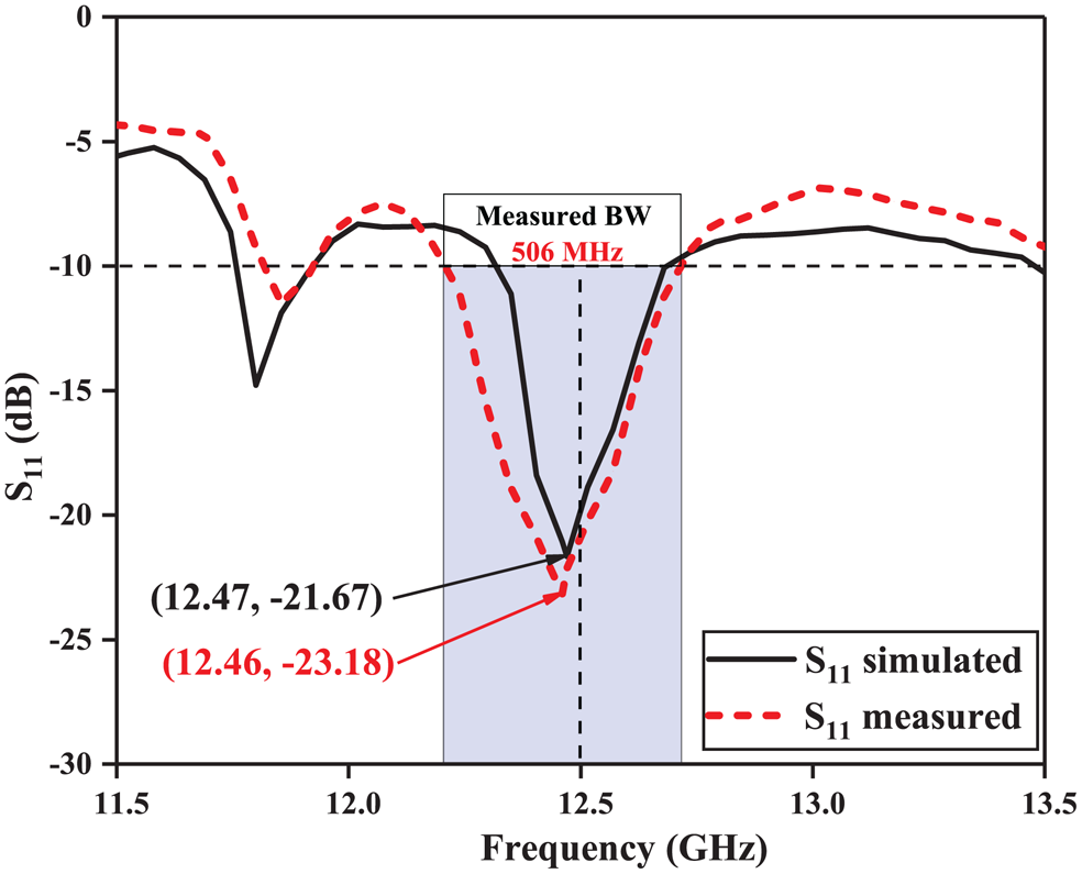
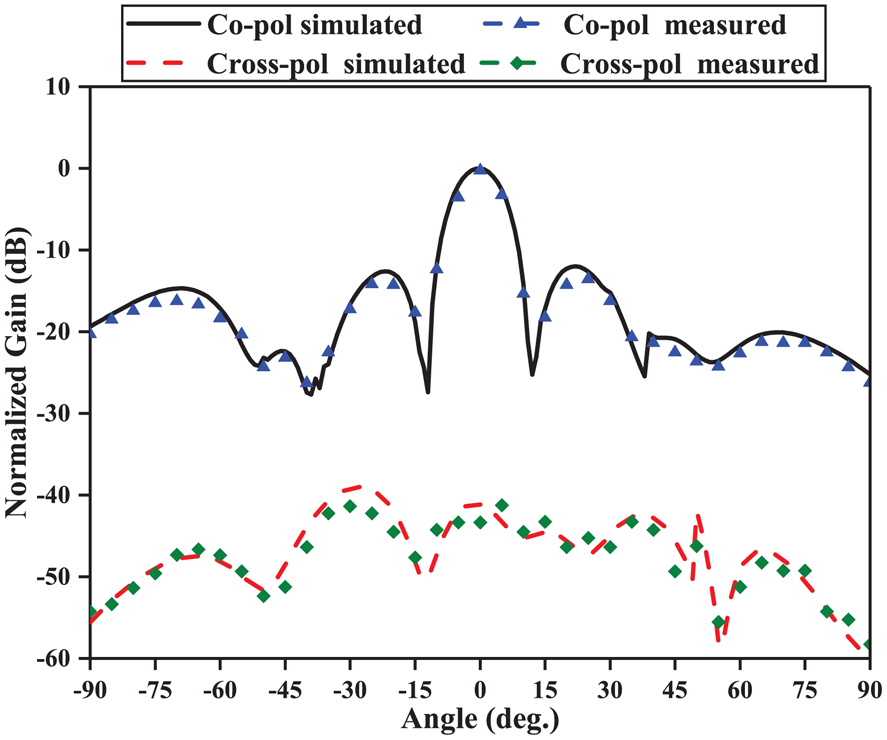
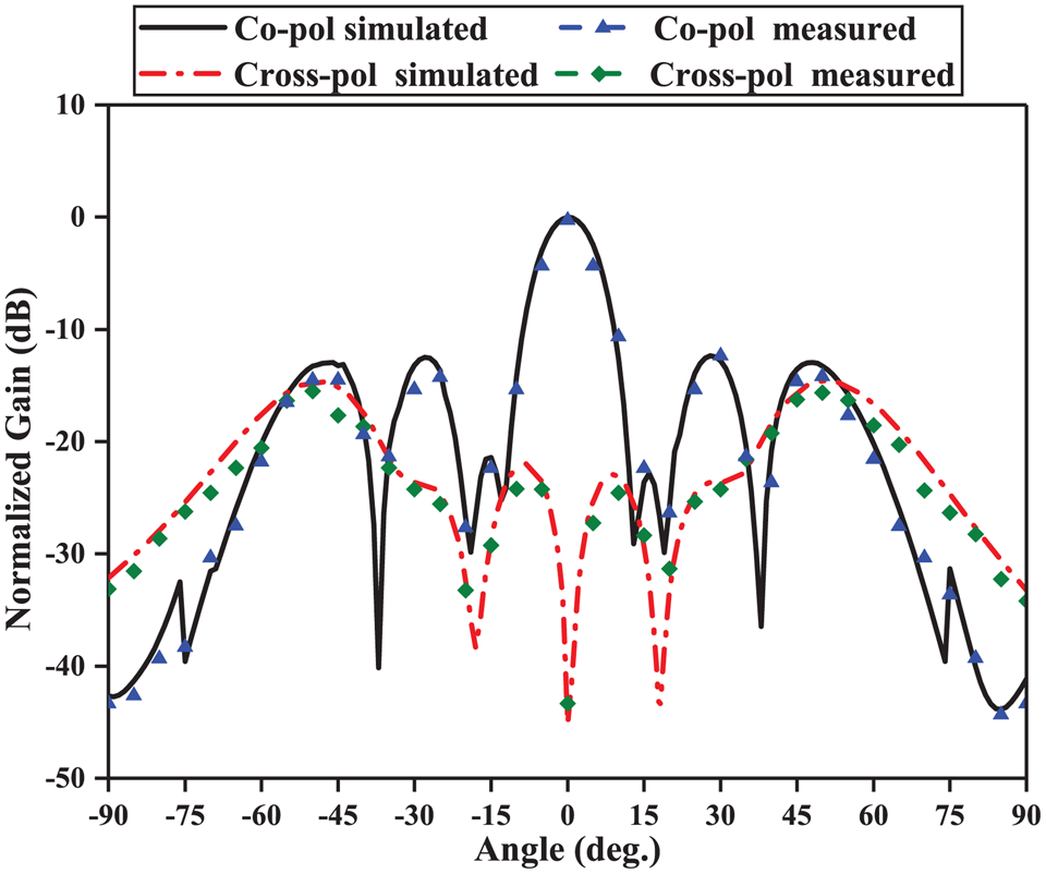
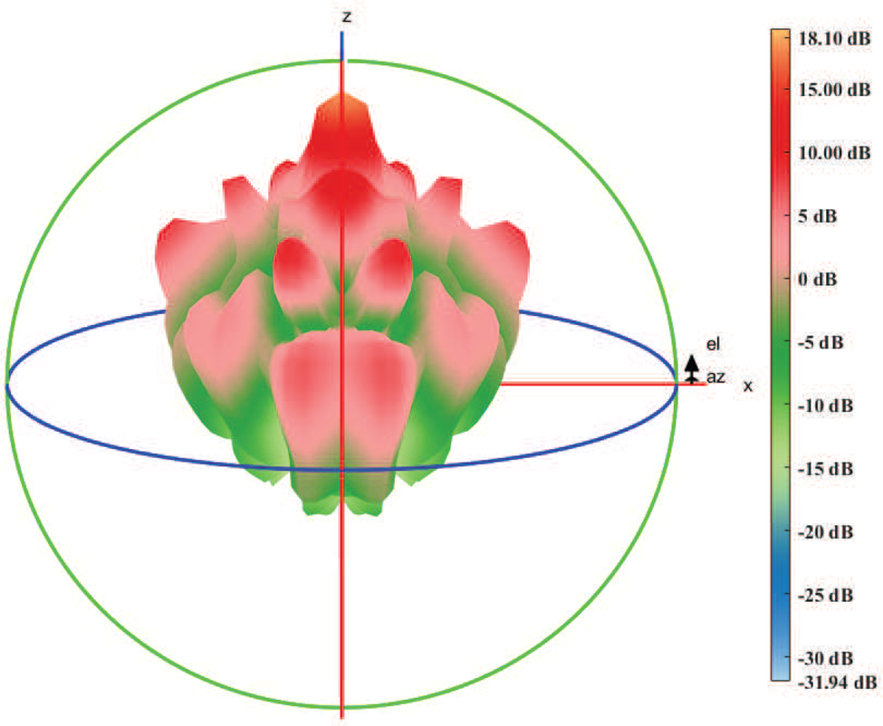
The gain, bandwidth, radiation efficiency (η), and aperture efficiency (ηap) of the proposed octagonal array are compared with the same parameters obtained from an eight-element linear array of proposed fractal radiating elements, as shown in Fig. 20(a). The inter-element spacing of the linear array is kept as 0.5λ and a simple branch type Wilkinson-Power divider has been implemented as the feed network. The simulated performance parameters are shown in Figs 20(b) and 20(c) respectively. The simulated gain of the linear array is 16.90 dBi whereas, the proposed octagonal array gives a simulated gain of 18.10 dBi. The simulated bandwidth of the linear array is 324 MHz whereas, the proposed octagonal array gives a bandwidth of 340 MHz. The simulated radiation efficiency(η) and aperture efficiency (ηap) of the linear array are: 84.14 and 65.26% respectively, whereas the proposed octagonal array gives simulated values of η and ηap as 84.50 and 73.63% respectively. Therefore, the proposed octagonal array outperforms than the linear array in terms of gain, bandwidth, radiation efficiency and aperture efficiency. Inspired from these results, the octagonal array has been fabricated. The fabricated array prototype is shown in Fig. 21 and its corresponding measured reflection coefficient is depicted in Fig. 22. The measured bandwidth of the array prototype from Fig. 22 is recorded as 506 MHz. The E- and H-plane radiation patterns of the array are shown in Figs 23 and 24 respectively. The measured values of the maximum SLL of the array, from E- and H-plane radiation pattern is − 15.20 dB and measured first null beamwidth is 23.20°. The directivity of the fabricated structure becomes 18.87 dBi [Reference Balanis1]. The measured gain of array is obtained as 17.67 dBi as shown in Fig. 19. All performance parameters of the single element and the array are shown in Table 5, which also reflect a very good agreement between simulated and measured results. The 3D radiation pattern of the octagonal array is shown in Fig. 25. It can be observed from Fig. 25, that the main beam of the array is oriented along the z- axis at an angle of θ = 0°, which indicates that beam of the array has not been scanned to a particular direction, and hence no progressive phase shifts has been given among the elements.
Array of spiral-based fractal antennas: (a) array arrangement, (b) simulated return loss, and (c) simulated parametric results.

Fabricated antenna array prototype.

Reflection coefficient of the array.

E-plane co- and cross-polarization radiation patterns of the array.

H-plane co- and cross-polarization radiation patterns of the array.

3D radiation pattern of the array.

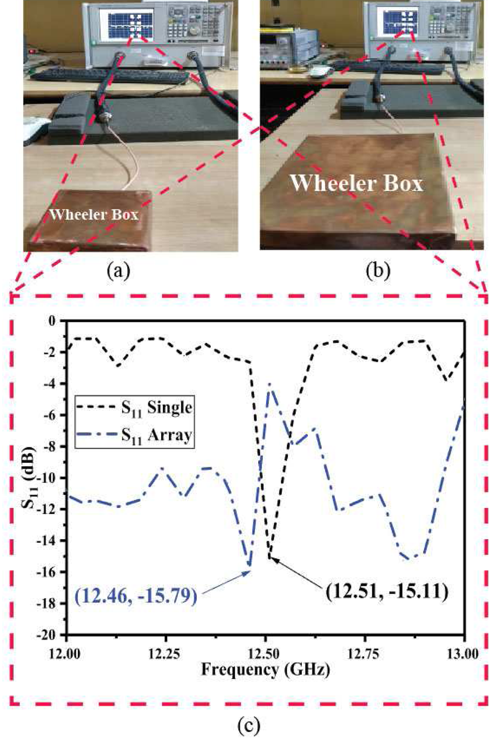
The efficiency of the fabricated single element as well as the array are computed using Wheeler's method [Reference Wheeler38,Reference Moharram and Kishk39] and are shown in Figs 26(a) and 26(b). The reflection coefficient (RL) of the single element as well as the array with cap are recorded from Fig. 26(c) respectively. The RL without the cap for both single element as well as for the array are already previously recorded as mentioned in Table 5. The efficiency (η) of the fabricated structures are obtained from these recorded values of return losses, with and without the metal caps, using Wheeler's method [Reference Wheeler38,Reference Moharram and Kishk39]. These caps are designed using copper plates of thickness 0.56 mm with dimension of 8 × 8 × 5 cm3 for the single element, and 17 × 18 × 5 cm3 for the array. Following the Wheeler's method, the measured efficiency of the single element at 12.51 GHz is obtained as $\eta = 86.70\percnt$ and for the array, it is $\eta = 82.20\percnt$
 at 12.46 GHz.
Efficiency measurement using Wheeler-cap: (a) single element, (b) array, and (c) magnifying portion of S 11 with cap.

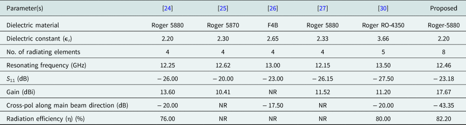
A comparative performance of the proposed array is shown in Table 8. Moreover, the single-layered structure of the proposed array ensure more stable S 11 performance [Reference Balanis1; Reference Pozar33], less bulky, much easier to fabricate in compared with other arrays in the literature.
Comparative performance of the fabricated array prototype

NR, not reported.
Conclusion
A compact, linearly polarized octagonal array is designed for DBS application. The single element of the array is derived from a 2D spiral-shaped fractal geometry and it poses 2D quadrantal symmetry. The single element of this array is a new fractal antenna which gives quite a decent gain of 9.32 dBi, and is capable of heavily suppressing cross polarization along the main beam direction. The measured value of cross polarization of the single element is − 45.50 dB along the main beam. The cross polarization suppression is achieved without employing the most commonly used techniques of tampering the ground plane of the structure, which is having the tendency to shift the resonating frequency and reduce the gain of the antenna. The feed network of the array makes the structure very compact. The fabricated single element as well as array prototypes reflects a very good agreement between the simulated and measured results.
Acknowledgments
This publication is an outcome of the Research work undertaken under SERB Extra Mural Research Funding (File No.: SB/S3/EECE/226/2016), Department of Science and Technology, Government of India.
 Kalyan Sundar Kola completed M.Tech in ECE from NIT Durgapur, West Bengal, India in 2014. Since 2018, he is working as an Institute Research Scholar at the National Institute of Technology Goa, Farmagudi, Ponda, Goa, India. His research area includes microstrip fractal patch antennas, antenna with DGS structure, miniaturized antennas, array of fractal antennas, dual-band array antennas, and shifted-beam antenna array.
 Anirban Chatterjee received his M.Tech and Ph.D. from the National Institute of Technology, Durgapur, India in 2009 and 2013, respectively. Presently, he is working as an Assistant Professor in the department of ECE at the National Institute of Technology Goa, Farmagudi, Ponda, Goa, India. His research interest includes array antennas, soft computing, and image frequency rejection techniques in modern receiver systems. He has published 17 research papers in international journals and 8 papers in international conferences. He has received Gandhian Young Technological Innovation (GYTI) appreciation award in 2019.
 Deven Patanvariya received his M.Tech degree in electronics and communication engineering from the National Institute of Technology Goa in 2017. He is currently working as a JRF in the ECE department at the National Institute of Technology Goa, Farmagudi, Ponda, Goa, India.