I. INTRODUCTION
The perovskite oxides have conductivities that vary from metallic to semiconducting to insulating, and they possess an extremely diverse range of optical, electronic, and magnetic properties that include ferroelectricity, ferromagnetism, piezoelectricity, and superconductivity. Reference Chambers1,Reference Ngai, Walker and Ahn2 Integration of these oxides with semiconductors could open up many opportunities for novel device functionalities. Reference Demkov and Posadas3 These intriguing possibilities have garnered considerable attention during the past decade, especially given the relatively simple perovskite cubic structure and the close in-plane lattice-matching with common semiconductors such as Si, Ge, and GaAs. However, perovskite oxides cannot be easily deposited directly onto semiconductor surfaces, mostly because of differences in the bonding of the two types of material. Moreover, oxidation of semiconductor surfaces under normal oxide growth conditions is likely to cause severe degradation of the anticipated electrical properties since any amorphous interfacial layer would prevent direct oxide-semiconductor contact. A successful strategy to overcome this serious bottleneck in fabricating epitaxial oxide-heterostructures has been developed that involves depositing a sub-monolayer of Sr metal onto the clean Si surface. Reference McKee, Walker and Chisholm4 This layer inhibits oxidation while also providing an initial nucleation template for growth of a thin ‘buffer’ layer of SrTiO3 (STO) that can in turn be used as a composite pseudosubstrate for further epitaxial oxide growth. Reference Demkov, Ponath, Fredrickson, Posadas, McDaniel, Ngo and Ekerdt5
Progress in developing and exploiting novel types of advanced materials has historically been closely tied to the availability of adequate measurement and characterization facilities. Thus, instrumentation capable of providing detailed information about atomic location and chemical identity becomes invaluable when probing oxide-semiconductor heterostructures. The sub-Ångstrom wavelength of the high-energy beam of the electron microscope offers the prospect of comparable spatial resolution, but the unavoidable spherical aberration of conventional magnetic electron lenses was for many years a major obstacle that limited electron-microscope performance. Revolutionary breakthroughs in aberration correction hardware have been achieved, Reference Haider, Uhlemann, Schwan, Rose, Kabius and Urban6,Reference Krivanek, Dellby and Lupini7 enabling spatial resolution and information limits well beyond the previously insurmountable 1-Å barrier to be obtained. Reference O'Keefe8,Reference Dahmen, Erni, Radmilovic, Kisielowski, Rossell and Denes9 In addition, the field-emission electron sources of these aberration-corrected instruments enhance the analytical signal quality so much that compositional analysis is nowadays achievable in special cases even to the level of single-atom identification. Reference Krivanek, Chisholm, Nicolosi, Pennycook, Corbin, Dellby, Murfitt, Own, Szilagyi, Oxley, Pantelides and Pennycook10,Reference Zhou, Kapetanakis, Prange, Pantelides, Pennycook and Idrobo11 These extreme levels of imaging and analytical performance have the potential to dramatically transform current knowledge and understanding of many types of emerging materials. This paper provides an overview of our recent observations of oxide-semiconductor heterostructures using the technique of aberration-corrected scanning transmission electron microscopy (AC-STEM). The perovskite oxides observed include strontium titanate (SrTiO3—STO), barium titanate (BaTiO3—BTO), and strontium hafnate (SrHfO3—SHO), grown on either Si(001) and/or Ge(001) substrates.
II. EXPERIMENTAL DETAILS
All of the oxide-semiconductor heterostructures described here have been grown using either molecular-beam epitaxy (MBE) or atomic-layer deposition (ALD), techniques that are described in detail elsewhere. Reference Demkov, Ponath, Fredrickson, Posadas, McDaniel, Ngo and Ekerdt5,Reference McDaniel, Ngo, Hu, Posadas, Demkov and Ekerdt12 MBE is widely recognized as the ideal technique for growing epitaxial layers of well-controlled stoichiometry and excellent crystallinity. For the samples described here, the MBE growth has been carried out using a customized DCA-600 system with a base pressure of 3 × 10⁻¹⁰ Torr. This system is equipped with six effusion cells, an electron-beam evaporator, and an atomic oxygen plasma source. Elemental Sr, Ti, and Ba are typically evaporated from effusion cells at 450, 1700, and 570 °C, respectively, with molecular oxygen used as the oxidant, resulting in deposition rates calibrated by a quartz crystal monitor on the order of one atomic layer per minute. During deposition, the substrate is radiatively heated from behind using an SiC-based heating element. Reflection-high-energy electron diffraction (RHEED) is used routinely throughout to monitor the crystallinity and stoichiometry of the growth surface.
ALD is an alternative growth technique that enables thin-film growth at relatively low temperature and low cost, making it appealing for industrial applications. The ALD growth for the present samples has been carried out using a custom-built, hot-wall stainless-steel chamber that is pumped out by a turbo-molecular pump to a base pressure of below 1 × 10⁻⁶ Torr. During ALD growth, the precursor(s) and the carrier/purge gas (usually argon) are introduced through a manifold at the front of the chamber, with continuous evacuation during deposition using a dual-stage rotary-vane pump and an operating pressure of ∼1 Torr. The precursors used for ALD growth were barium bis(triisopropylcyclopentadienyl), titanium tetraisopropoxide, strontium bis(triisopropylcyclopentadienyl), and hafnium formamidinate, with water as the oxidant.
Most of the samples reported here have been characterized in situ without air exposure by x-ray photoelectron spectroscopy (XPS) using a VG Scienta R3000 electron energy analyzer (VG Scienta, Tonbridge, United Kingdom). X-ray diffraction (XRD) with a Philips X'pert double-crystal diffractometer (FEI Company, Eindhoven, The Netherlands) is also routinely used ex situ to determine the crystallographic orientations and lattice constants of the various perovskite films relative to the (001) substrate normal. Further sample-specific growth information for the respective oxide-semiconductor heterostructures is provided below.
All samples were prepared for electron-microscope observation in the cross-section geometry using standard mechanical polishing and dimpling, followed by argon-ion-milling, initially at ∼4.0 to 4.5 keV and finally at ∼2.0 to 2.5 keV, to achieve foil perforation. The AC-STEM images were mostly recorded with a JEOL ARM-200F operated at 200 keV (JEOL Ltd., Akishima, Japan). The beam convergence angle was typically set at ∼20 mrad, while collection angles were 0–22 mrad for (incoherent) large-angle bright-field (LABF) imaging and 90–150 mrad for high-angle annular-dark-field (HAADF) imaging. The electron-beam directions used for observation were [110] for the Si and Ge substrates, and [100] for the oxide layers, corresponding to the expected 45° in-plane rotation between the semiconductor-oxide crystal lattices. A spatial resolution of better than (1/4) a Si = 0.136 nm is required for these observations, in order to resolve individual atomic columns of Si (or Ge).
III. RESULTS
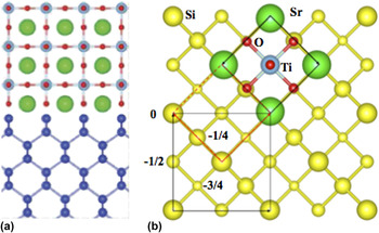
To appreciate the relatively simple geometry at least in principle of the perovskite oxide-semiconductor interface, it is instructive to represent the interfacial atomic arrangements in terms of a simple ‘ball-and-stick’ model. The cross-section view shown in Fig. 1(a) illustrates the situation where the [110] projection of the substrate is aligned with the [100] projection of the oxide, while the orthogonal plan-view projection is illustrated in Fig. 1(b). This orientation relationship arises from the geometrical relationship a Ge/Si/√2 ≈ a perovskite. The room-temperature lattice parameters for the perovskite oxides are a = 3.905 Å for SrTiO3, and a = 3.992 Å and c = 4.036 Å for BaTiO3, respectively, while the reduced a/2〈110〉 in-plane lattice-spacings of Si and Ge are 3.841 Å and 4.001 Å, respectively. Thus, the epitaxial oxide growth on the substrate surface can result in either compressive or tensile strain, depending upon which semiconductor is used as the substrate, as well as providing control over the in-plane or out-of-plane polarization direction of the oxide thin film: examples of the latter will be shown later.
Ball-and-stick models showing approximate atomic arrangements across the perovskite oxide-semiconductor interface: (a) cross-section view; (b) plan-view. The 45° in-plane rotation of the oxide lattice relative to the underlying semiconductor brings almost exact two-dimensional registry of the two crystal lattices.

A. STO on Si using MBE
The epitaxial growth of STO on Si(001) substrates has historically been of interest based on the need for an alternative high-k dielectric material for transistor devices, Reference Wilk, Wallace and Anthony13 while more recent attention has turned to the potential suitability of STO/Si as a pseudosubstrate for the growth of other perovskite oxides. Reference Reiner, Kolpak, Segal, Garrity, Ismail-Beigi, Ahn and Walker14 The STO/Si interface has been intensively studied but the atomic-scale structure at the interface remains unclear, as described in detail elsewhere. Reference Wu, Aoki, Posadas, Demkov and Smith15 This uncertainty prompted us to carry out a systematic AC-STEM study of thin (∼5 unit cells) STO layers grown directly on Si(001) substrates by MBE, with a particular focus on the nature of defects that either relieve misfit strain (STO on Si is compressively strained by ∼1.7%) or help to accommodate lattice mismatch across atomic-layer steps of the substrate surface that are incommensurate with the oxide lattice structure. During sample preparation, careful attention was given to remove the substrate surface oxide, which was followed by deposition of a half-monolayer of Sr at a pre-calibrated rate of 1 monolayer per minute before co-deposition of Sr and Ti to the desired thickness under suitable oxygen partial pressure, and annealing under vacuum at 550 °C. Further particulars of the substrate surface treatment and the growth process are given elsewhere. Reference Wu, Aoki, Posadas, Demkov and Smith15
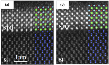
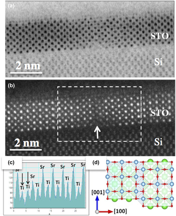
Figures 2(a) and 2(b) show HAADF images of the STO/Si interface in cross-section, overlaid with schematics that show the corresponding atomic structure which can be determined by direct inspection of the images. The interface appears to be sharp, and there are no signs of interfacial reactions or an intermediate oxide layer. The Si substrate shows closely spaced pairs of Si atomic columns in the bulk (often referred to as “dumbbells”), whereas the Si substrate surface shows two different terminations (i.e., half Si dumbbells or full Si dumbbells) for the two different images. In both situations, it is clear that the rows of Ti atomic columns in the SrTiO3 epilayer are aligned directly above the rows of Si atomic column(s) at the interface with. Figures 3(a) and 3(b) are LABF and HAADF images, respectively, which show a vertical offset within the STO thin film that seems to be directly connected with the presence of a step at the substrate surface. The intensity line profile from the HAADF image, shown in Fig. 3(c), indicates that there are two immediately adjacent planes of Ti atomic columns, forming an anti-phase boundary (APB). Figure 3(d) is a schematic structural model depicting the vertical APB offset. Further observations of the STO–Si heterostructures also revealed APB-type defects in the absence of surface steps, consistent with the view that these APBs could also result from the merger of crystalline domains originating from random nucleation sites on the substrate surface. Structural analysis indicated that these APBs occurred on either [110] or [010] planes, with displacement vectors of a STO/2〈110〉 in both cases. Reference Wu, Aoki, Posadas, Demkov and Smith15
Probe-corrected HAADF STEM images showing cross-section of SrTiO3/Si interface together with overlaid models showing corresponding atomic structure: (a) single Si atomic columns at interface; (b) double Si atomic dumbbells at interface.

(a) LABF STEM, and (b) HAADF STEM, aberration-corrected images of MBE-grown SrTiO3/Si heterostructure showing vertical offset (arrowed) within SrTiO3 thin film attributed to presence of APB defect. (c) Lateral intensity line profile from within boxed area in (b) showing adjacent Ti atomic columns (arrowed). (d) Structural model of APB defect in SrTiO3 showing vertical offset of adjacent Ti atomic columns.

B. STO on Ge using MBE
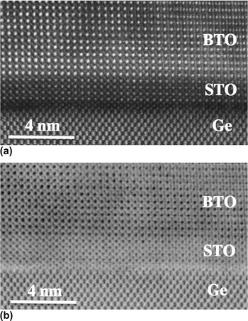
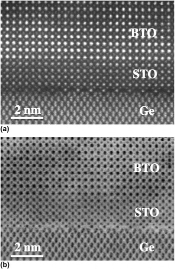
Thin epitaxial layers of SrTiO3 provide invaluable buffer layers for the growth of other perovskite oxides. The epitaxial growth of STO on Ge(001) substrates rather than Si (001) substrates is not as difficult nor so challenging to achieve in comparison with oxide growth on Si because Ge surfaces are not so easily oxidized. Surface contamination for Ge substrates can be removed chemically, and oxygen-plasma cleaning followed by thermal annealing in situ within the MBE chamber has been shown to remove any remaining surface carbide and oxide, Reference Ponath, Posadas, Hatch and Demkov16 which is usually confirmed by the appearance of surface reconstruction spots visible in RHEED patterns. Deposition of half-monolayers of either Sr or Ba is again used to prevent the Ge surface from oxidizing during the subsequent MBE growth of the STO buffer. Figures 4(a) and 4(b) are a complementary pair of HAADF and LABF STEM images, respectively, showing a typical region of a BTO/STO/Ge heterostructure grown by MBE. Reference Ponath, Fredrickson, Posadas, Ren, Wu, Vasudevan, Okatan, Jesse, Aoki, McCartney, Smith, Kalinin, Lai and Demkov17 The STO/Ge interface is abrupt and free of any amorphous interlayer, and the substrate surface layer is terminated by single Ge atomic columns aligned with the Ti atomic columns in the epilayer above. In comparison, Figs. 5(a) and 5(b) are HAADF and LADF images showing another region of the BTO/STO/Ge heterostructure. The initial plane of atoms in the STO layer shows a highly characteristic double periodicity along the interface caused by the atomic columns of Sr, and the uppermost pair of Ge atoms displays a distinct 2× periodicity, with the Ge dumbbells showing a pronounced inward slant toward each other. This tilted appearance of the rows of Ge dimers is exactly what might be predicted to be visible when viewing along the Ge(001) 2 × 1 reconstructed surface at glancing angle. Finally, it is significant that the BTO layer is confirmed as compressively strained to the STO buffer layer, and it shows out-of-plane polarization, which is the preferred orientation for fabrication of ferroelectric field-effect transistors. Reference Ponath, Fredrickson, Posadas, Ren, Wu, Vasudevan, Okatan, Jesse, Aoki, McCartney, Smith, Kalinin, Lai and Demkov17
(a) HAADF STEM, and (b) LABF STEM images showing region of MBE-grown BaTiO3/SrTiO3/Ge heterostructure.

(a) HAADF STEM, and (b) LABF STEM images from region of MBE-grown BaTiO3/SrTiO3/Ge heterostructure showing sharp STO–Ge interface with 2× periodicity corresponding to [110]-type projection of Ge(001) 2 × 1 surface reconstruction.

C. BTO on Ge using MBE
Preparation of the Ge(001) substrate prior to deposition of BaTiO3 follows the same basic procedure as outlined above for STO growth, all the way through to RHEED observations confirming the 2 × 1 surface reconstruction. Reference Fredrickson, Ponath, Posadas, McCartney, Aoki, Smith and Demkov18 A protective layer consisting of a half-monolayer of Sr or Ba is again deposited before actually initiating MBE growth of the BTO layer to prevent any surface oxidation. After removal of the as-grown oxide-semiconductor heterostructure from the growth chamber, XRD is normally used to measure lattice constants and to confirm the relative crystallographic orientations. Measurements of the BTO–Ge heterostructures indicated that the shorter a-axis of the BTO film is out-of-plane [i.e., (100)-oriented], with the ferroelectric polarization field pointing along an in-plane direction.
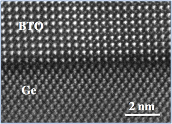
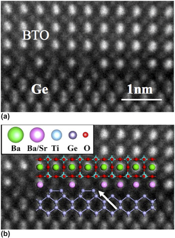
Aberration-corrected images of the BTO–Ge heterostructures clearly show clean and abrupt interfaces. Individual Ba and Ti(O) atomic columns are visible in the BTO films and the projected dumbbell structure of the Ge atomic columns is readily apparent, as shown by the example in Fig. 6. Extensive observations of the BTO–Ge interface region show that the Ge surface has both 1× and 2× periodicities, indicating that the Ge 2 × 1 reconstruction has been retained during deposition and subsequent growth of the BTO thin film. Moreover, as revealed by the enlargement and superimposed structural model shown in Fig. 7, single-layer steps of the Ge surface often correspond to locations where the surface periodicity in projection changed from 1× to 2×. This unambiguous confirmation of the enduring nature of the surface reconstruction, with its characteristic inward slant of the projected Ge dimer pair, proved to be crucial in enabling close agreement to be obtained between calculated and measured conduction-band offsets, which theoretical modeling had shown previously to be highly sensitive to the interfacial atomic arrangements. Reference Fredrickson, Ponath, Posadas, McCartney, Aoki, Smith and Demkov18
Probe-corrected HAADF STEM image showing region of MBE-grown BaTiO3/Ge heterostructure with abrupt interface and single interfacial Ge atomic columns.

(a) Enlarged view of BaTiO3/Ge interface with both 1× and 2× periodicities visible along the interface plane; (b) same image with overlaid structural model. Arrow indicates position of Ge surface step with transition between 1× and 2× periodicity of reconstructed Ge(001) surface as viewed along [110]-type projection. Reference Wu, Aoki, Posadas, Demkov and Smith15

D. BTO on Ge using ALD
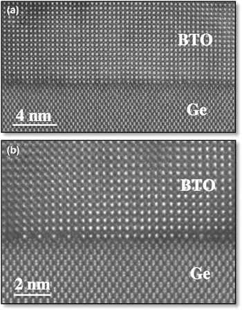
The superior electronic performance of germanium in terms of increased hole and electron mobilities, makes Ge an attractive substrate material for many device applications. Thus, the possibilities for growth of crystalline BaTiO3 thin films directly on Ge(001) substrates using the ALD technique have been investigated. Reference McDaniel, Ngo, Posadas, Hu, Lu, Smith, Yu, Demkov and Ekerdt19 Following thermal de-oxidation of the Ge wafer under ultrahigh-vacuum (UHV) conditions, as described above for the MBE-grown samples, RHEED observations at reduced temperature were again used to confirm the presence of the 2 × 1 reconstruction of the Ge(001) surface. Transfer to the ALD growth chamber in vacuo was followed by thin-film growth to the desired thickness at growth temperatures typically of ∼225 °C, followed by thermal annealing at 650 °C under UHV conditions to achieve crystallization. Figure 8(a) is a HAADF STEM image showing part of a BTO–Ge heterostructure grown by the ALD technique. The interface is again abrupt, as observed already for the samples grown by MBE, and the Ti atomic columns in the BTO thin film line up directly opposite the single atomic columns of Ge. Figure 8(b) is another HAADF STEM image showing an interfacial region where there is clear transition from 1× to 2× periodicity at the Ge surface, which is located at the position of a Ge surface step. Overall, these images confirm the viability of the ALD growth technique as the basis for fabricating advanced oxide-semiconductor heterostructures. Reference McDaniel, Ngo, Posadas, Hu, Lu, Smith, Yu, Demkov and Ekerdt19
Probe-corrected HAADF STEM images showing cross-sections of ALD-grown BaTiO3/Ge heterostructure: (a) single Ge atomic columns line up directly opposite Ti atomic columns in the BTO thin film; (b) enlargement showing interfacial region with transition from 1× to 2× periodicity corresponding to the position of a Ge(001) surface step.

E. SHO on Ge using ALD
The small to negligible band offsets of BTO and STO with Si and Ge have stimulated renewed interest in alternative high-k dielectric oxides. SHO is a suitable candidate material, especially given its close lattice-match (∼1.9% mismatch) with Ge. Thus, ALD growth has been used in fabricating SHO–Ge heterostructures. Reference McDaniel, Hu, Lu, Ngo, Posadas, Jiang, Smith, Yu, Demkov and Ekerdt20 The Ge substrates were first degreased and then exposed to ultraviolet light for 30 min prior to annealing in vacuo to achieve the 2 × 1 (001) surface reconstruction, as observed by RHEED, before transfer into the ALD chamber to enable deposition of the SHO film. Postdeposition annealing was carried out at substrate temperatures in the range of 650–850 °C, with concurrent real-time RHEED observations to monitor the transition from amorphous to crystalline structure. XPS was also used in situ to determine the valence-band offset and to evaluate the oxidation state and stoichiometry of the SHO film, which typically varied in the range of 52–56% Sr for the cation sub-lattice. Further details of the ALD growth, as well as information about the initial testing of capacitor structures used to extract dielectric constant and to evaluate interface trap states, can be found elsewhere. Reference McDaniel, Hu, Lu, Ngo, Posadas, Jiang, Smith, Yu, Demkov and Ekerdt20
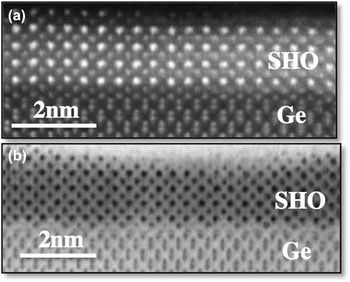
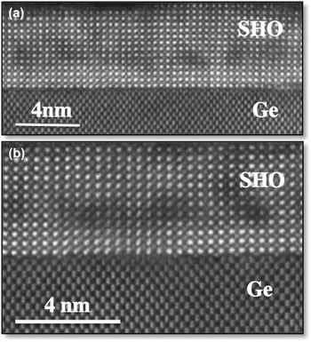
Electron microscopy has provided useful complementary information along the path toward trying to establish the optimum conditions for growth and annealing treatments. Figure 9 shows examples of cross-sectional images from a 2-nm-thick SHO film annealed at 650 °C for 5 min. The HAADF STEM image in Fig. 9(a) shows a region where the 1× periodicity of the Ge(001) surface is clearly apparent, while the LABF STEM image in Fig. 9(b) shows a predominant 2× periodicity, both for the Ge substrate surface and the initial layer of the oxide film. Figure 10 shows two HAADF STEM images from a 5.2-nm-thick SHO film annealed at 700 °C for 5 min. The lower-magnification image in Fig. 10(a) indicates some nonuniformity in the SHO film in the region located about 2–4 nm above the SHO–Ge interface, most likely associated with local variations in stoichiometry. The enlarged image in Fig. 10(b) shows an ill-defined arrangement of Ge and Sr atomic columns at the interface plane, located between two areas showing 2× periodicity of both the substrate surface and the initial plane of the oxide film. These observations confirm the abruptness of the SHO–Ge interface and the excellent crystallinity of the ALD-grown SHO film. Furthermore, electrical measurements suggest that there could be significant advantages for Hf-based perovskites over Ti-based perovskites for advanced electronic device applications. Reference McDaniel, Ngo, Posadas, Hu, Lu, Smith, Yu, Demkov and Ekerdt19
(a) HAADF STEM image of ALD-grown SrHfO3/Ge heterostructure showing region where Ge(001) surface shows 1× periodicity; (b) LABF STEM image of ALD-grown SrHfO3/Ge heterostructure showing region where Ge(001) surface shows predominant 2× periodicity.

(a) HAADF STEM image of ALD-grown SrHfO3/Ge heterostructure showing contrast variations likely due to compositional fluctuations in region located about 2–4 nm above the SHO/Ge interface; (b) enlarged view of interface region surface showing ill-defined interface structure in between two regions with clear 2× periodicity of the Ge substrate surface.

IV. CONCLUDING REMARKS
These observations of perovskite oxide-semiconductor heterostructures using the technique of probe-corrected scanning transmission electron microscopy have provided greatly improved information about the atomic arrangements across their complex interfaces. In all samples studied, matching pairs of (incoherent) LABF and HAADF images are recorded simultaneously, and the structural information that can be extracted is comparable. However, defects are more easily located at low magnification in LABF images due to the presence of strain contrast that is invisible in HAADF images. Moreover, we find that the intensity of LABF images is less sensitive to atomic number Z than the corresponding HAADF images. Reference Aoki, Lu, McCartney and Smith21 Conversely, structural arrangements at defects as well as oxide-semiconductor interfaces seem more intuitively interpretable in HAADF images, as demonstrated, for example, in Figs. 4 and 7. However, for comparison with theoretical modeling, further microscopy studies are still needed to improve the precision with which the atomic locations are located. For example, locating cation column positions with a precision of 5 p.m. has been demonstrated, Reference Jia, Mi, Urban, Vrejoiu, Alexe and Hesse22 and achieving close to 1 p.m. should be possible with some local averaging and assuming precise control and correction of lens aberrations. Concurrent spectroscopy studies (albeit at lower beam energy due to the likelihood of beam-induced sample damage) are also being used to determine the extent of any chemical interdiffusion. Meanwhile, it is abundantly clear from the results presented here, and described in detail elsewhere, that the MBE and ALD growth techniques represent viable routes toward achieving monolithic integration of oxides and semiconductors.
ACKNOWLEDGMENTS
This work has primarily been supported by the Air Force Office of Scientific Research through Grants FA9550-12-10494 and FA9550-14-10090 and the National Science Foundation Award CMMI-1437050. The authors gratefully acknowledge the use of facilities in the John M. Cowley Center for High Resolution Electron Microscopy at Arizona State University.