I. INTRODUCTION
Wear-resistant ceramic components are essential to modern industry. Ever-higher demands on these components and new technological possibilities are driving the development of new wear-resistant materials. It is not surprising that extremely wear-resistant materials are typically based on materials containing diamond or cubic boron nitride (cBN). Over the last few years the costs of diamond grit has dropped strongly, making new applications possible. The main disadvantage of these materials is the need to manufacture them using high-pressure synthesis, which limits their use due to high costs and geometrical restrictions. Reference Rödel, Kounga, Weissenberger-Eibl, Koch, Bierwisch, Rossner, Hoffmann, Danzer and Schneider1–Reference Haines, Leger and Bocquillon3 Hence, lower-cost superhard materials and technologies for manufacturing them are highly sought after. Manufacturing of SiC-bonded diamond materials represents a promising way to obtain low-cost, superhard, wear-resistant materials. Reference Voronin, Zerda, Gubicza, Ungar and Dub4–Reference Matthey, Höhn, Wolfrum, Mühle, Motylenko, Rafaja, Michaelis and Herrmann18
SiC–diamond composites can be produced through reactive sintering of powders or infiltration of diamond preforms with silicon. Requirements for preparing dense, fine-grained materials by reaction sintering of diamond and silicon powder can be quite elaborate. Ko et al. Reference Ko, Tsurumi, Fukunaga and Yano6 prepared dense polycrystalline samples with diamond grain sizes of less than 1 µm and SiC bonding by high-pressure sintering at 6 GPa. Reaction sintering of fine-grained diamond materials has been performed using the capsule HIP method. However, it does result in a certain amount of residual porosity. Reference Shimono and Kume7 This is caused by the large volume change accompanying the reaction of silicon with diamond or carbon to form SiC and the high rate of this reaction. The use of coarser diamond grain sizes decreases the reaction rate. Hot pressing of Si–SiC–diamond materials with a diamond grain size of 100 µm has been described in the literature. Reference Zhu, Lang and Ma16 However, these materials exhibit a relatively high content of unreacted silicon.
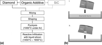
An alternative route of preparing SiC-bonded diamond materials is the infiltration by liquid silicon without pressurization (Fig. 1). The resultant materials contain approximately 50% by volume of diamond embedded in a three-dimensional skeleton of β-SiC. Reference Ekstrom and Gordeev9–Reference Herrmann, Matthey, Kunze and Petasch14 Besides diamond and SiC, unreacted free silicon is contained in these materials. The microstructures formed in such materials were recently reviewed. Reference Matthey, Höhn, Wolfrum, Mühle, Motylenko, Rafaja, Michaelis and Herrmann18 It was shown that epitaxial growth of the SiC on flat surfaces of diamond takes place. The orientation relationship {111}diamond‖{111}3C–SiC and 〈011〉diamond‖〈112〉3C–SiC was observed for these materials. This corresponded to a tilt of 30° of the {111} planes of diamond and 3C–SiC, resulting in a minimal lattice mismatch. This epitaxial growth was observed despite the fact that the diamond particles were originally covered by nondiamond carbon formed by pyrolysis of the organic binder before silicon infiltration. By high-resolution TEM analysis, 5- to 20-nm-thick turbostratically disordered layers were observed at the interface between diamond and silicon carbide, further reducing the lattice mismatch between these components. The strong chemical bonding between the diamond grains and the SiC skeleton are the reason for the high strength and wear resistance. In contrast, the nano-sized β-SiC grains observed on rough diamond surfaces indicated a different growth mechanism. Thin graphitic interfaces were observed at infiltration temperatures above 1600 °C, resulting in a reduction in hardness and wear resistance. Reference Herrmann, Matthey, Höhn, Kinski, Rafaja and Michaelis12
Schematic view of the preparation of SiC bonded diamond materials: (a) flow chart for preparation of the SiC bonded diamond materials, (b) schematic view of the dipping process for applying a SiC bonded diamond surface layer (After Reference Herrmann, Matthey, Kunze and Petasch14 ).

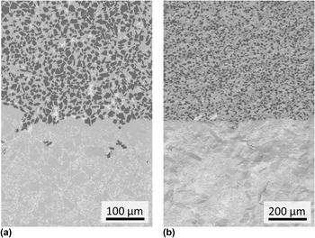
Apart from compact materials, graded materials and components can be prepared by combined infiltration of diamond and SiC preforms. These components consist of a conventional SiSiC body with a diamond–SiC composite layer with a thickness of 0.1 mm to a few millimeters on the functional surfaces (Figs. 1 and 2). Reference Herrmann, Matthey, Höhn, Kinski, Rafaja and Michaelis12–Reference Herrmann, Matthey, Kunze and Petasch14 The objective of the present work was to review the current state of the art of these composites.
Typical microstructures of SiC bonded diamond material and the SiSiC materials with SiC bonded diamond surface layer (a) produced by pressing with 10 µm diamonds, (b) by dip coating. The present phase can be identified by gray value, dark—diamond, gray—SiC and light gray—silicon.

II. RAW MATERIALS AND CHARACTERIZATION METHODS
For the preparation of the diamond preforms, synthetic diamond powders (VDiamant Ltd., Seddiner See, Germany) with different average grain sizes of 5, 10, 20, 50, and 100 µm were used as starting powders. The content of metallic impurities of the used diamond powders were less than 0.05 wt%. For shaping of the preforms two different organic binders novolac resin and cellulose binder were used.
The green body pore size distribution was analyzed using Hg porosimetry (Micromeritics, Aachen, Germany). The density in the pyrolyzed state was determined using the dimensions of the samples and the weight. For the reacted materials, the density was measured by the Archimedes method.
The phase content was determined using X-ray diffraction (XRD; D8 Advance, Bruker AXS Ltd., Karlsruhe, Germany). XRD measurements were carried out with Cu Kα radiation and with a position-sensitive detector (PSD) LynxEye (Bruker AXS Ltd., Karlsruhe, Germany) in the 2θ range between 10° and 120°. Quantitative phase analysis was carried out using image analysis of polished cross sections.
For microstructural characterization, the composite samples were prepared using ion beam techniques Reference Höhn, Sempf and Hermann19 due to the inapplicability of conventional mechanical preparation methods for artifact-free preparation of the interfaces between the hard diamond phase and the softer SiC-matrix. The microstructures of the samples were investigated using an NVision 40 scanning electron microscope (Carl Zeiss SMT Ltd., Oberkochen, Germany) equipped with focused ion beam gun for preparation of thin samples and a STEM detector as well as an energy-dispersive X-ray (EDS) detector.
Material strength was determined using an Instron 8562 (Instron Ltd., Darmstadt, Germany) in four-point bending in accordance with DIN EN 843-1 and the ball-on-triple-ball method on discs with a diameter of 30 mm and a sample height of 2–3 mm according to the method developed by Danzer. 20 At least five samples were tested for each condition.
The fracture toughness was determined using the SEVNB method according to DIN CEN/TS 14425-5. The V-notch was introduced either by laser cutting or in the pyrolyzed state. Both methods gave the same results following correction for measurement uncertainty.
The corrosion behavior was determined using bending bars (3 × 4 × 45 mm) of bulk diamond–SiC composite as well as SSiC and SiSiC reference materials in an aqueous solutions of 20 wt% NaOH at a temperature of 90 °C. The corrosion depth was measured at different times in scanning electron microscope on fractured cross sections of the bending bars. The details are given in Ref. Reference Herrmann, Kluge, Rödel, Mc Kie and van Staden32.
The cavitation resistance was tested by using an ultrasonic oscillator whose tip was placed 0.5 mm above the sample. The whole setup was placed in a thermostated glass beaker at 20 °C filled with distilled water. During the testing, the temperature increased up to 30 °C due to the high energy input caused by the oscillating tip. The tip of the ultrasonic oscillator was 13 mm in diameter and vibrated with a frequency of 20 kHz and an amplitude of 50 µm. The test was carried out in time intervals of two hours, totaling in 10 h.
Oscillating wear tests were carried out using the SRV200 (Optimol Instruments Ltd., Munich/Germany) in a ball-on-disk configuration under dry sliding conditions (30–50% relative humidity and temperature of 22 °C). The wear tests were conducted through application of different normal forces (20, 60, and 100 N) at a sliding speed of 0.04 mm/s and a stroke length of 2 mm. A steel ball (100Cr6, Ø 10 mm) and a silicon nitride ball (Ø 9 mm) were used as counterbodies. Prior to the wear tests each sample was cleaned in an ultrasonic bath with acetone.
III. MATERIALS PREPARATION
A. Processing and shaping
The materials and the components were produced using conventional ceramic technologies analogous to those used to produce SiSiC. Investigations performed up to now at Fraunhofer IKTS have focused on dry pressing and casting of composites with diamond grain sizes of 5–100 µm. The schematic diagram in Fig. 1(a) illustrates the technology used.
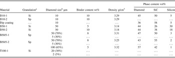
Diamonds were mixed with the corresponding binders and solvents and granulated or were processed into suspensions for casting. Novolac resins or a cellulose binder were used as binders for granulating the diamonds for subsequent pressing. Granulation of the diamonds was carried out by spray-drying of water-based suspensions with a cellulose binder; smaller quantities were produced using ethanol-based diamond suspensions and Novolac resins (Table I). The granules produced could be used for both graded (see Fig. 2) and ungraded materials. For the graded composites, standard SiSiC granules were additionally used for the substrate material (see Fig. 2).
Composition of the material, density and phase content observed after infiltration (measured by image analysis).

a Si—ethanol based sieve granulation, Sp—spray dried granules.
b In brackets the volume fraction of the different diamond fractions.
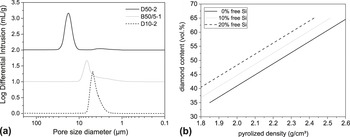
The materials were compacted by die pressing at pressures of 40–100 MPa. The densities and mean pore sizes after pyrolysis are given for the different diamond grain sizes and polymodal mixtures in Fig. 3. The resultant pore structure was strongly influenced by the diamond grain size and the compaction pressure and was found to be a major factor determining the infiltration kinetics (see below). The final green density could be determined directly from the diamond content in the final material under the assumption that full infiltration took place [Fig. 3(b)].
(a) Pore size distribution in the pyrolyzed preform determined by Hg-porosimetry as a function of the diamond grain size (uniaxial pressing with 40 MPa), (b) diamond content in the infiltrated material as a function of the green density and the residual Si-content.

Production of components by dry pressing limits the grading possibilities. Therefore, dip coating was also tested as an alternative process. Shaped pyrolyzed SiC preforms or even infiltrated SiSiC preforms served as “casting molds” on which diamond layers were deposited [Fig. 1(b)].
The slurry requirements and the process parameters are determined mainly by the desired thickness of the diamond layer to be applied. Thicknesses for dip-coated layers were in the range of 100–500 µm. Coatings with a higher thickness could be generated through repeated dipping and drying. For defect-free coating of sharp-edged surfaces and large areas by dip coating, the binder used for the slurry was based on a nontoxic aqueous dispersion of a thermoplastic polyvinyl ester.
For the preparation by die pressing, even large diamond grains can be used. For the casting or dipping process, the grain size is limited due to the settlement of the larger diamonds. Therefore, composites with diamond grain sizes of only up to 50 µm were prepared so far.
After shaping, the organic binder was removed by pyrolysis. In this thermochemical process, which takes place with the exclusion of oxygen, the binder decomposes into carbon and volatile compounds. A non-diamond carbon framework is formed during pyrolysis, generating sufficient bonding of the diamond particles for green machining of the components. Due to the fact that the bonding of the diamond particles occurs through the pyrolyzed binder, binders with a high residual carbon content are preferable. The Novolac resin had a residual carbon content of approx. 50–55 wt%, whereas the value for water-based cellulose binder was just 30 wt%.
The carbon framework formed during pyrolysis reacted with infiltrated silicon to form SiC in the subsequent silicon infiltration step.
B. Infiltration and microstructure formation
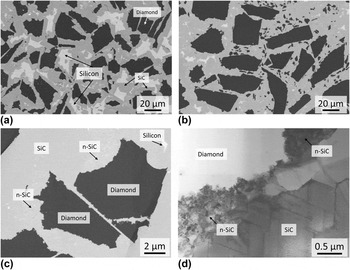
The materials listed in Table I were infiltrated at 1600 °C in a vacuum for 0.5 h and were completely dense. Besides diamond, 3C–SiC and free silicon were observed by microstructural and XRD analysis. The microstructure consisted of diamond grains embedded in a three-dimensional SiC framework. Unreacted, residual silicon could be found in the interstices between some of the SiC grains (Figs. 2 and 4).
SEM-micrograph of D50-2-material (a) B50/5-1 (b) D10-1 in higher magnification to represent the details of microstructure (c) and STEM image of sample D10-1 for investigation of the nanocrystalline interface region (d).

Silicon infiltration into the preforms is analogous to the preparation of SiSiC 20–Reference Cohrt22 and carbon preforms Reference Greil, Lifka and Kaindl23–Reference Zollfrank and Sieber25 but has a number of special features.
Reaction of diamond with the infiltrated silicon to form SiC is accompanied by a volume increase of 266% (129% for reaction with graphite), which leads to rapid closing of the infiltration channels and, in the worst-case scenario, to incomplete silicon infiltration. The changes in the external dimensions of the materials are less than 0.3%. The closing of the channels during infiltration results in constraints concerning packing density and minimum pore channel diameter. The achievable infiltration depth for silicon in porous diamond preforms is lower for a smaller diamond grain size due to the higher reactivity and the lower pore sizes. This results in infiltration depths of several tens of millimeters for shaped bodies with diamond grain sizes of >10–20 µm but only 1–2 mm or less for a diamond grain size of 2–5 µm with a similar packing density. Reference Mlungwane, Herrmann and Sigalas10,Reference Herrmann, Matthey, Kunze and Petasch14
The reaction of silicon with diamond or graphite is strongly exothermic:
 $${\rm{Si}} + {{\rm{C}}_{{\rm{(diamond)}}}} \to {\rm{SiC}}\quad \Delta {H_{(1500\,^\circ {\rm{C}})}} = - 74.12\;{\rm{kJ/mol}}\quad.$$
This exothermic reaction causes localized heating of the sample, which can accelerate the reaction of the carbon with silicon and hence the closing of pore channels. In addition, for diamond composites, transformation of diamond to graphite can be initiated at a temperature T > 1600 °C. Reference Matthey, Höhn, Wolfrum, Mühle, Motylenko, Rafaja, Michaelis and Herrmann18 No α-SiC, which usually forms at temperatures above 1900 °C, was formed in the infiltrated samples. Together with the absence of graphite formation in materials infiltrated below 1600 °C, this is an indication of the absence of strong internal heating during infiltration. This could be due to the high thermal conductivity of the diamond and the lower reactivity of the diamond in comparison with that of pyrolytic carbon.
The interaction between diamond and liquid silicon results in very rapid formation of a layer of SiC on the diamond. The surface layer consists of 4- to 6-µm-thick well-faceted platelet-shaped crystals epitaxially grown on the diamond surface. This epitaxial growth takes place despite the fact that the diamond surface is coated with pyrolytic carbon. Most probably, the pyrolytic carbon dissolves quickly in the liquid silicon melt, thereby saturating it with carbon and subsequently precipitating as SiC nuclei on the diamond surfaces. Simple calculations show that during infiltration 15–21 wt% of the initial carbon in the preform reacts with the melt (assuming a material containing 50 vol% of diamond and 20 or 0% free silicon). This amount is much more than the reactive pyrolytic carbon formed by the pyrolysis of the binder (less than 10 wt%). Therefore, no nondiamond carbon was found in the materials and some of the diamond had to be dissolved in the silicon and reacted with it to form SiC.
The morphology of the formed SiC grains and the orientation relationship between SiC and diamond provide evidence of the fast lateral growth of silicon carbide on the flat surfaces of the diamond, with carbon being transported through the liquid silicon. Reference Matthey, Höhn, Wolfrum, Mühle, Motylenko, Rafaja, Michaelis and Herrmann18
This is different from the phase formation observed during the infiltration of biomorphic carbon. In these materials, a nanocrystalline SiC layer is first formed during infiltration. Reference Zollfrank and Sieber25 Besides the different solution kinetics of diamond and non-diamond carbon, the different stresses of the nuclei could be the reason why a nanocrystalline SiC layer is first formed during infiltration of biomorphic carbon with silicon. In the SiC-bonded diamond materials, areas of nanocrystalline SiC grains mixed with residual silicon are only formed in regions in which rough diamond surfaces are observed [Figs. 4(c) and 4(d)]. These nanocrystalline grains also have a special orientation in relation to the diamond grains, indicating that these SiC grains were also formed epitaxially on the diamond. Reference Matthey, Höhn, Wolfrum, Mühle, Motylenko, Rafaja, Michaelis and Herrmann18
The present experiments revealed that after the SiC layer thickness of 4–6 µm was reached on the diamond surface, the reaction rate declined strongly. Reference Herrmann, Matthey, Höhn, Kinski, Rafaja and Michaelis12,Reference Matthey, Höhn, Wolfrum, Mühle, Motylenko, Rafaja, Michaelis and Herrmann18,Reference Mlungwane, Sigalas, Herrmann and Rodrıguez26 However, Yang et al. Reference Yang, He, Wu, Zhang and Ma15,Reference Yang, He, Wu, Zhang, Ma, Liu, Hu, Zhang and Qu17 describe the time dependence of the thickness with a simple parabolic law without passivation. Sangsuwan et al. Reference Sangsuwan, Tewari, Gatica, Singh and Dickerson27 proposed a complex model involving a fourth-power rate law of the time for the SiC growth on glassy carbon. The present results and also a critical analysis of the data in the literature Reference Sangsuwan, Tewari, Gatica, Singh and Dickerson27 suggest that there is a change in the mechanism after the layer has formed. Therefore, after the complete covering of the diamond, reaction of the residual free silicon with diamond is controlled by diffusion through the grains or through the grain boundaries between the SiC grains. The rate of the diffusion processes can be estimated by means of the determined diffusion coefficients for diffusion of Si and C in the SiC lattice and in the grain boundaries. Reference Hon and Davis28,Reference Hon, Davis and Newbury29 Extrapolating these data to lower temperatures yields D C = 10−14 cm2/s at 1600 °C (carbon diffusion is faster than the diffusion of silicon). The diffusion-controlled growth through a SiC layer can be described under steady-state conditions by the Fick’s law Reference Barsoum30 as:
 $$J = - D{{\Delta C} \over x}\quad ,$$
where J is the flux, ΔC is 3.5 g/cm3 (concentration of carbon in diamond with the assumption of a very low concentration of C in the liquid silicon), D is the coefficient of self-diffusion in SiC, and x is the thickness of the SiC layer.
The increase in thickness of the SiC layer is connected with the flux by Eq. (2):
 $${{{\rm{d}}x} \over {{\rm{d}}t}} = J{{{M_{{\rm{SiC}}}}} \over {{M_{\rm{C}}}{\rho _{{\rm{SiC}}}}A}} = J{{40\;{\rm{g}}} \over {12\;{\rm{g}} \times {{3.2\;{\rm{g}}} \over {{\rm{c}}{{\rm{m}}^3}}}1\;{\rm{c}}{{\rm{m}}^2}}} = J \times 1.04\;{\rm{cm/g}}\quad.$$
Replacing J in Eq. (2) by Eq. (1) and integration of Eq. (2) yields the following (with x = x 0 at t = 0):
 $${x^2} = - 1.04D\Delta Ct + x_0^2\quad.$$
For a 2 µm-thick SiC layer, an increase of only 3 nm is obtained in 1 h. This is a strong indication that the SiC layer growth by this mechanism has a very low rate.
The carbon diffusion along the grain boundaries is approximately six orders of magnitude higher (10−8 cm2/s at 1600 °C), resulting in a transport along the grain boundaries that is three orders of magnitude higher. Reference Hon and Davis28,Reference Hon, Davis and Newbury29 In the SiC-bonded diamond materials, the typical lateral dimensions of the SiC platelets are on the order of the diamond grain size, i.e., several µm. Therefore, the concentration of the grain boundaries is too low to result in a significant increase in the thickness of the formed SiC layer during infiltration.
However, for nanocrystalline SiC as is formed during silicon infiltration of biomorphic carbon materials, the diffusion along the grain boundaries can result in a significant reaction of free silicon by this mechanism. The rapid passivation of the diamond surface by the SiC layer leads to the stabilization of the diamond but also to incomplete reaction of the silicon if the pores in the pyrolyzed state have maximum diameters larger than twice the thickness of the layer. That is, for large grains with a unimodal grain size distribution, large pores in the preform are formed (diameter of the pore in a close-packed sphere structure is 0.41 of the diameter of the sphere and hence approximately 20 µm for preforms with a diamond grain size of 50 µm). This is also the reason why the material prepared from the unimodal 50 µm diamonds has the high silicon content [Table I and Fig. 4(a)]. The cross section of the microstructure of this material [Fig. 4(a)] clearly shows the relatively thin SiC layers around the diamonds and the large pools of remaining silicon. Increasing the amount of binder (see materials D50-1 and D50-2 in Table I) or using bimodal or multimodal diamond grain size distributions (B50/5, T100) as shown by the different materials in Table I and Fig. 4(b) can minimize this effect. Using this approach, the diamond content in the infiltrated material could also be increased.
Detailed analysis of the microstructure of the materials infiltrated at 1550 °C (Fig. 4) reveals full infiltration but also the absence of non-diamond carbon at the interface. This was proved by X-ray diffraction, Raman spectroscopy and high resolution SEM investigations. Details concerning the interface between diamond and SiC are described in the literature. Reference Matthey, Höhn, Wolfrum, Mühle, Motylenko, Rafaja, Michaelis and Herrmann18
IV. PROPERTIES
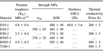
An overview of the properties of the SiC-bonded diamond materials obtained in the present work is given in Table II. Measurement of mechanical properties was restrained by the fact that conventional grinding technologies were not feasible for the given materials. Flat surfaces could be machined only by time-consuming lapping. Most of the bending bars tested failed at defects on the surfaces or the chamfers. The test geometry was therefore changed to the ball-on-triple-ball (B3B) configuration to allow for testing of sandblasted samples. The data given in Table II were determined for sandblasted surfaces. These surfaces are quite similar to those of various wear parts. Therefore, the strength results reflect the behavior of possible components.
Properties of different SiC-bonded diamond materials.

The strength values determined by the B3B method were slightly higher than the values obtained for the bending bars. This was due to the edge effects of the bending bars as well as to slight differences in loaded volume between the two methods.
The strength values obtained for the D50 material containing diamonds with a grain size of 50 µm were lower than those obtained for the D10-1 and D10-2 materials containing 10 µm diamonds. In contrast, the material B50/5-1 and B50/5-2 containing also diamonds with a grain size of 50 µm but shows strength values in the range of the samples D10-1 and D10-2. Evidence for this was provided by the fact that B50/5 materials containing bimodal diamond distributions (50 and 5 µm) has only a content of residual silicon of 2–3 wt%. Therefore, the lower strength can be related with a higher silicon content in the material. This high silicon content was most probably also the reason for the lower fracture toughness (Table II).
The observed strength values of the materials with the low silicon content were very similar to the strength of SSiC materials measured by Harrer et al., Reference Harrer, Danzer and Rendtel31 who found strengths of 489–653 MPa for lapped or polished sintered SiC samples.
These high strength values correlated with the measured fracture toughness values (obtained using the SEVNB method) given in Table II. SiC–diamond materials exhibit higher fracture toughness levels than that of SiC due to internal stresses in the materials, which have been detected by Raman spectroscopy, Reference Herrmann, Matthey, Höhn, Kinski, Rafaja and Michaelis12,Reference Zerda, Wieligor, Ungar and Palosz33 as well as the formation of nanocrystalline areas at the interfaces between diamond and the SiC matrix. These stresses result in additional reinforcement mechanisms such as crack deflection or crack branching. Analysis of the fracture surfaces showed that the cracks mainly ran through the diamond grains, reflecting the strong bonding of the diamond in the material.
Table II also shows the thermal conductivity values. The thermal conductivity of these materials was high and increased with increasing diamond grain size. Accordingly, the material containing a large fraction of 100 µm diamond grains exhibited a value of 500 W/(m K). These materials can thus be used for wear applications as well as for thermal management systems.
For ungraded SiC–diamond materials, the wear was found to be lower than that of hardmetals and B4C by a factor of more than 30 for machining of stones or highly filled plastics. Reference Larsson, Axen, Ekström, Gordeev and Hogmark34 Measurements of wear resistance of the D10-1 and D10-2 materials in sandblasting conditions (DIN 50332/ETEC standard with corundum particles F40, a pressure of 5 bar, an angle of 90°, and a distance of 45 mm) revealed low wear for these materials. The wear of the D10 materials was about a factor of 30 lower than that of Al2O3 materials and at least ten times lower than the wear of commercial B4C ceramics.
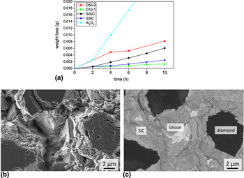
The cavitation stability of the materials was tested in comparison with different commercial alumina and SiC ceramics. The resistance to cavitation is an important parameter for components used in pumps and bearings. The results obtained for the materials D10-1 and D50-2 are shown in Fig. 5(a).
Results of the cavitation experiments (a) weight loss as a result of cavitation of D50-1 and D10-1 in comparison to two Al2O3- and SiSiC and SSiC reference materials and (b, c) SEM micrograph of the surface of the material D10-1material after cavitation experiments (SE- and ESB images).

The D10 material showed a much higher resistance than that of SiSiC materials and the same level as that found in sintered silicon carbide materials. The D50-3 material showed a lower resistance. This could be attributed to the high silicon content of the material. According to the micrographs of the worn surface [Fig. 5(b)], the silicon was primarily removed by cavitation. The D50 material contained 18% by volume of residual silicon, whereas the D10 material contained only 5% by volume. No preferential damage of the SiC–diamond interface took place. Only after prolonged cavitation did the SiC grains start to be destroyed by microcrack formation.
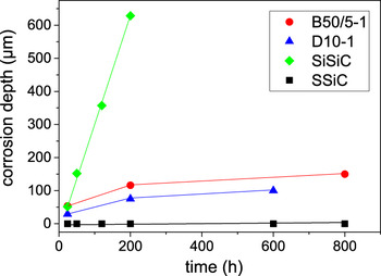
A high silicon content is also critical for the corrosion resistance under hydrothermal conditions and in hot basic solutions. The corrosion resistance is much higher for materials with silicon contents in the range of 5 vol% than for SiSiC materials. The resistance of the SiC bonded diamond materials is more similar to the high corrosion resistance of SSiC materials. Reference Herrmann, Matthey, Kunze and Petasch14,Reference Herrmann, Kluge, Rödel, Mc Kie and van Staden32
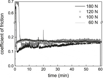
Investigations of the tribological properties of these materials in oscillating sliding tests with steel and Si3N4 balls as mating bodies demonstrated the great potential of this class of materials. The friction coefficients (COFs) against Si3N4 balls are given in Fig. 6. The COF for SiC materials under the same conditions is 0.6 against steel and Si3N4 balls. Blug et al. Reference Blug, Hörner, Matthey and Herrmann35 measured CVD diamond coatings under the same conditions. For these materials, a similar COF of 0.15 was observed. Although the SiC-bonded diamond materials only contain approximately 50% by volume of diamond, they exhibit wear resistance levels similar to that of polycrystalline diamond (PCD). This is caused by the fact that the wear of SiC is slightly higher than that of diamond. Therefore, after the run-in period the diamond is higher than the surrounding SiC is and the counterbody is only in contact with the diamond grains. The diamond hence controls the wear of the composite. Similar behavior was recently observed for diamond–Si3N4 composite materials. Reference Wolfrum, Quitzke, Matthey, Herrmann and Michaelis36
Friction coefficient of the material D50-2 during oscillating sliding against a 12.7 mm (diameter) Si3N4-ball as a function of time and the applied load (humidity 20%).

The corrosion resistance of SiC-bonded diamond materials is similar to that of sintered SiC ceramics (SSiC) in acids. Reference Harrer, Danzer and Rendtel31 In basic solutions, the corrosion resistance strongly depends on the residual silicon content. The materials with a free silicon content of less than 5 vol% showed a much higher resistance than that of typical SiSiC materials. After initial dissolution of the silicon in the near-surface area, no further damage took place (Fig. 7). Thus, corrosion resulted in only a very moderate reduction in strength due to the strong SiC–diamond skeleton. Reference Herrmann, Kluge, Rödel, Mc Kie and van Staden32
Thickness of the corrosion layer of the materials D50-1 and D10-1 as a function of time in 1 mol NaOH solution at 90 °C in comparison to SiSiC and SSiC.

V. CONCLUSIONS/SUMMARY
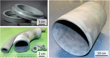
SiC-bonded diamond prepared by pressureless infiltration of diamond preforms represents a promising new class of materials with wear behavior that is much superior to that of hard metal and conventional ceramics. The material can be monolithic or laminated/graded, with layers 0.3 mm to several mm in thickness formed on the SiSiC substrate. The composite can be produced either by conventional infiltration of the SiSiC and diamond preforms or by deposition of the silicon carbide-bonded diamond layer on infiltrated SiSiC components by dipping technologies and subsequent infiltration. However, the slurry-based layers show a slightly lower diamond content and are limited in terms of possible diamond grain size. Large wear parts can be produced with a cost-effective technology. Figure 8 gives some examples of components prepared using these technologies.
Components produced from SiC bonded diamond materials. Sealing rings (top left) and SiSiC materials with surface layer from SiC-bonded diamond produced by dipping: inliner of an attrition mill (right) and different tubes (bottom left).

To generate SiC-bonded diamond materials with high wear resistance, strength, and corrosion resistance, the content of free silicon has to be minimized. Materials with 4–5% by volume residual silicon can be reproducibly produced. To achieve this, it is necessary to optimize the grain size distribution of the diamonds in the preforms as well as the binder content.
The selection of a suitable silicon infiltration regime can completely avoid the formation of graphite layers at the diamond–SiC interface and hence achieve a strong bond between the diamond grains and the matrix. The epitaxial growth of the SiC on the diamond surfaces results in strong interfaces and the material consists of three-dimensional SiC and diamond skeletons, resulting in the high wear and corrosion resistance and a strength level similar to that of typical SSiC materials.
ACKNOWLEDGMENTS
The results presented here were generated in projects financed by the German Federal Ministry of Education and Science (BMBF) 37 and by the BMWi/AIF based on a decision of the German Bundestag (parliament).