Initial strain-mediated magnetoelectric studies
In 1961, Astrov first measured the magnetoelectric (ME) effect in chromium oxide (Cr2O3),Reference Astrov1 verifying an effect predicted only a few years prior by Landau, Lifshitz, and Dzyaloshinskii.Reference Dzyaloshinskii2 Over the next 40 years, several new materials and some particulate composites displaying the ME effect were developed.Reference Rado and Folen3–Reference Rado, Ferrari and Maisch9 However, they mostly possessed small ME coupling that vanished above cryogenic temperatures, inhibiting their use in applied technologies. The field took a new direction in 2001 after Ryu et al. created a laminate composite sandwiching the piezoelectric material PZT (Pb[ZrxTi1–x]O3) between two layers of magnetoelastic Terfenol-D (Tb0.3Dy0.7Fe1.92).Reference Ryu, Carazo, Uchino and Kim10 This composite approach worked at room temperature and exhibited ME coupling almost two orders of magnitude stronger than any previous work. Within only a few years, coupling up to seven orders of magnitude stronger than Cr2O3 had been reported using strain-mediated ME composites.Reference Jahns, Piorra, Lage, Kirchhof, Meyners, Gugat, Krantz, Gerken, Knöchel and Quandt11–Reference Zhai, Dong, Xing, Li and Viehland13
A strong understanding of the physics governing this phenomenon was critical to obtain strong ME coupling. Initial macroscale studies demonstrated the existence of optimal bias strain/field conditions,Reference Wu, Chung, Chang, Keller and Carman14–Reference Hockel, Wu and Carman18 reduced coupling due to shear-lag and demagnetization fields,Reference Chang and Carman19 and demonstrated that the largest coupling strengths were attained by exciting a mechanical resonance.Reference Jahns, Piorra, Lage, Kirchhof, Meyners, Gugat, Krantz, Gerken, Knöchel and Quandt11–Reference Zhai, Dong, Xing, Li and Viehland13,Reference Wu, Chang, Chung and Carman17,Reference Nan, Bichurin, Dong, Viehland and Srinivasan20 Optimal bias conditions exist due to the nonlinear nature of the magnetoelastic component, in contrast to the linear piezoelectric material. Shear lag and demagnetization fields lead to inhomogeneous strain and magnetization distributions that prevent the whole composite from being in an optimally biased state. While ME materials by definition couple magnetic and electric fields, these findings indicate that the structural dynamics must be given equal consideration in strain-mediated ME composites. The macroscale findings have proven equally relevant at the micro-/nanoscale, and the strong coupling found in macroscale composites has translated into a highly energy-efficient method of controlling nanoscale magnetism. As a result, strain-mediated ME coupling is now actively being investigated as one of the most energy-efficient approaches to controlling nanoscale magnetism and may enable a paradigm shift in how we use magnets to store, transmit, and process information.
Strain-mediated control of magnetic domains
Initial experiments
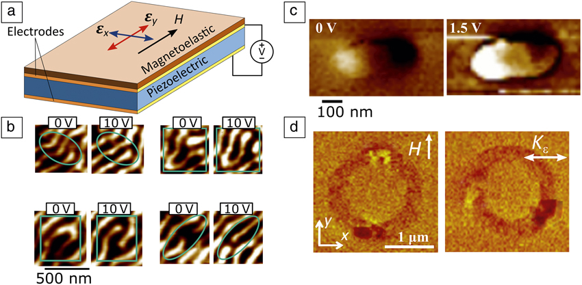
The control of micro-/nanoscale magnetic domains has been extensively studied during the past decade. Several geometries, including thin films,Reference Wu, Bur, Hockel, Wong, Chung and Carman21–Reference Chung, Wang, Chen, Lin, Chu, Lin and Hung24 bars,Reference Chung, Keller and Carman25 ellipses,Reference Buzzi, Chopdekar, Hockel, Bur, Wu, Pilet, Warnicke, Carman, Heyderman and Nolting26–Reference D’Souza, Fashami, Bandyopadhyay and Atulasimha30 and ringsReference Hockel, Bur, Wu, Wetzlar and Carman31,Reference Sohn, Nowakowski, Liang, Hockel, Wetzlar, Keller, McLellan, Marcus, Doran, Young, Kläui, Carman, Bokor and Candler32 have been investigated. Figure 1a schematically shows an experimental thin-film setup. A magnetoelastic film is deposited on a piezoelectric substrate. Applying a voltage to the substrate strains both materials, thereby controlling the magnetization. This control method is inherently different from conventional approaches that drive currents through small wires to create a magnetic field. Applying a voltage to a piezoelectric material (i.e., dielectric capacitor) dissipates significantly less energy than driving a large current through a metal by mitigating ohmic losses and relying on strong intrinsic piezoelectric and magnetoelastic coupling.
(a) Depositing a magnetoelastic film on a piezoelectric substrate enables voltage control of magnetism through strain-mediated magnetoelectric (ME) coupling. Magnetic force microscope (MFM) imaging has recorded ME control of domains in (b) thin-film, (c) single domain rod, and (d) ring geometries. In the MFM images (b–d) light regions are magnetized up and dark regions down (i.e., into and out of plane, respectively). In (b), enclosed green regions show domain walls curving, bending, branching, and elongating, respectively. The ME response in (c) (left to right) shows out-of-plane single domain rotation, and (d) (left to right) shows 90° rotation of an “onion-state” domain. Reprinted with permission from References Reference Chung, Carman and Mohanchandra23, Reference Chung, Keller and Carman25, and Reference Hockel, Bur, Wu, Wetzlar and Carman31. © 2008, 2009, and 2010 AIP Publishing. Note: εx and εy, in plane strain; H, magnetic field; K ε, induced magnetoelastic anisotropy; V, applied voltage.

Controlling magnetism in small structures is integral to the workings of several technologies (e.g., magnetic memory), and numerous nano-/microscale studies have demonstrated the usefulness of strain-mediated ME approaches. Figure 1b shows an early observation of strain-mediated ME domain wall control.Reference Chung, Carman and Mohanchandra23 Magnetic force microscopy (MFM) was used to observe the evolution of magnetic stripe domains in a nickel film on a PZT substrate. Figure 1c–d shows MFM images before (left) and after (right) applying voltage for (c) a single domain rodReference Chung, Keller and Carman25 and (d) ring geometry with a so-called “onion state” domain pattern.Reference Hockel, Bur, Wu, Wetzlar and Carman31 Voltage rotated the ring magnetization 90°, providing early evidence that strain-mediated coupling could switch between multiple states. Additionally, the size scale of these figures reveals strain-mediated control works in nanometer-sized regions. Modeling the coupled physics observed in these small elements has helped establish the key effects governing strain-mediated ME coupling, and led to strategies accurately controlling magnetic domains.
Modeling and control strategies
Micromagnetic simulations describe the evolution of magnetic domains in response to various stimuli. The dominant energies include the Zeeman ( ${U_{\rm{Z}}}$), magnetocrystalline (
 ${U_{{\rm{MCA}}}}$), exchange (
 ${U_{{\rm{Ex}}}}$), demagnetization (
 ${U_{{\rm{Demag}}}}$), and magnetoelastic (
 ${U_{\rm{\varepsilon }}}$) anisotropy.Reference Chikazumi33–Reference Liang, Keller, Sepulveda, Sun, Cui, Lynch and Carman36 The total magnetic energy density is:
 $$U = {U_{\rm{Z}}}\left( {{\bf{m}},{\bf{H}}} \right) + {U_{{\rm{MCA}}}}\left( {\bf{m}} \right) + {U_{{\rm{Ex}}}}\left( {\nabla {\bf{m}}} \right) + {U_{{\rm{Demag}}}}\left( {\bf{m}} \right) + {U_{\rm{\varepsilon }}}\left( {{\bf{m}},\,{\bf{\varepsilon }}} \right),$$
where  ${\bf{M}}$ is the magnetization, m the magnetic unit vector, H the magnetic field,
 ${\bf{\varepsilon }}$ the elastic strain, and the material is assumed to be locally saturated (i.e.,
 ${\bf{M}} = {M_s}{\bf{m}}$ and
 $\left| {\bf{M}} \right| = {M_s}$). The magnetoelastic anisotropy term provides the key coupling term for strain-mediated ME composites, where the strain is applied by a piezoelectric material.Reference Liang, Keller, Sepulveda, Bur, Sun, Wetzlar and Carman35–Reference Bur, Wu, Hockel, Hsu, Kim, Chung, Wong, Wang and Carman38 Equation 2 calculates the magnetoelastic energy density for a cubic material:
 $$\eqalign{ & {U_{\rm{\varepsilon }}} = {B_1}\left( {{{\rm{\varepsilon }}_{xx}}\left( {m_x^2 - {1 \over 3}} \right) + {{\rm{\varepsilon }}_{yy}}\left( {m_y^2 - {1 \over 3}} \right) + {{\rm{\varepsilon }}_{zz}}\left( {m_z^2 - {1 \over 3}} \right)} \right) + \ldots \cr & 2{B_2}({{\rm{\varepsilon }}_{xy}}{m_x}{m_y} + {{\rm{\varepsilon }}_{xz}}{m_x}{m_z} + {{\rm{\varepsilon }}_{yz}}{m_y}{m_z})\,, \cr}$$
where  ${B_1}$ and
 ${B_2}$ are the magnetoelastic anisotropy coefficients,
 ${m_i}$ are the components of the magnetization unit vector, and
 ${{\rm{\varepsilon }}_{ij}}$ are the components of the strain tensor (
 $i,j = \{ x,y,z\}$).
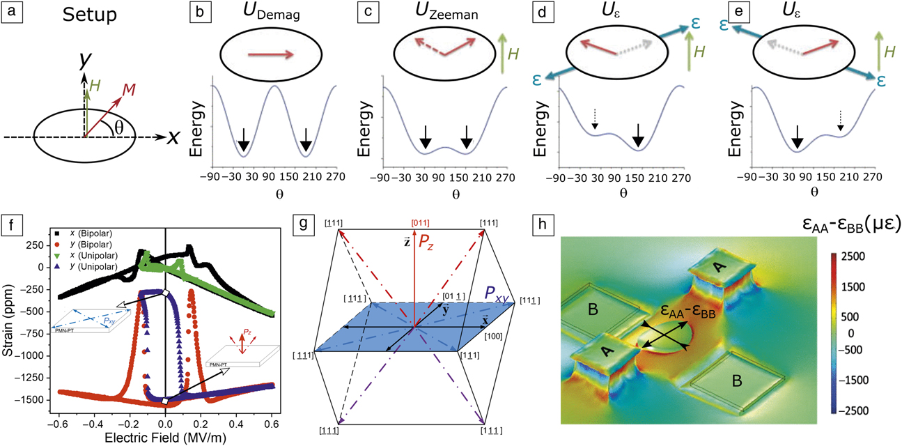
Figure 2a–e sequentially shows the effects of several energy terms in a two-dimensional thin-film ellipse and the resulting equilibrium orientations.Reference Liang, Keller, Sepulveda, Sun, Cui, Lynch and Carman36 The highlighted energies are the (b) demagnetization, (c) Zeeman, and (d–e) magnetoelastic anisotropy. A key point to highlight is that the energy landscape can have more than the two energy minima shown in this simple example. The energy minima are locations where the magnetization exists in equilibrium with the surrounding fields. For example, these critical points provide the nonvolatile equilibrium states for a magnetic memory bit (i.e., the 0 and 1 states). Applying strain deforms the energy landscape and allows the magnetization to switch states.
(a–e) The effects of multiple energies in a thin-film ellipse with the resulting equilibrium configurations (energy minima) highlighted by black arrows. The magnetic field and strain control local and global equilibrium orientations. Methods of applying biaxial strain include (f–g) using 011 cut Pb(Mg1/3Nb2/3)O3–PbTiO3 (PMN-PT) or (h) patterning local electrodes around magnetic elements. (f) Shows the strain along perpendicular x and y directions for electric field applied through the thickness of a PMN-PT plate. Bipolar means the electric field flips the ferroelectric polarization direction. Unipolar means the electric field never exceeds the polarization switching field. The unipolar y strain shows significant hysteresis, and insets show remanent polarization states with both in- and out-of-plane orientations existing (i.e., two stable equilibrium strain states at an electric field E = 0). (f) Rhombohedral structure of the (011) PMN-PT measured in (g), with relevant directions indicated. (h) Two pairs of electrodes (A and B) create biaxial strain εAA-εBB. The magnitude and orientation of εAA-εBB are controlled by the applied voltage. Reprinted with permission from References Reference Liang, Keller, Sepulveda, Sun, Cui, Lynch and Carman36 and Reference Wu, Zhao, Bao, Bur, Hockel, Wong, Mohanchandra, Lynch and Carman40. © 2014 and 2011 AIP Publishing. Note: ε, strain; H, magnetic field; M, magnetization; U Demag, demagnetization energy; U Zeeman, Zeeman energy;  ${U_{\rm{\varepsilon }}}$, magnetoelastic energy; P xy, XY polarization ; P z, Z polarization.
One key point emerging from thin-film models and experiments is that the magnetoelastic energy predominantly relies on the biaxial strain  ${{\rm{\varepsilon }}_{\rm{b}}} = {{\rm{\varepsilon }}_1} - {{\rm{\varepsilon }}_2}$, where
 ${{\rm{\varepsilon }}_1}$ and
 ${{\rm{\varepsilon }}_2}$ are the in-plane principal strains.Reference Bur, Wu, Hockel, Hsu, Kim, Chung, Wong, Wang and Carman38,Reference Lo Conte, Xiao, Chen, Stan, Gorchon, El-Ghazaly, Nowakowski, Sohn, Pattabi, Scholl, Tamura, Sepulveda, Carman, Candler and Bokor39 This means strategies to locally control the magnetic moment focus on controlling the biaxial strain state (e.g., applying tension in one direction and compression perpendicularly). Two primary methods of applying biaxial strains are illustrated in Figure 2f–h.
Figure 2f–g illustrates the biaxial strain generated by an 011 cut Pb(Mg1/3Nb2/3)O3-PbTiO3 (PMN-PT) substrate and relevant crystalline orientation. Wu et al. found giant anisotropic strain hysteresis, biaxial strains of  ${\rm{\varepsilon }}_{\rm{b}} \approx 2000\,{\rm{\mu }}\varepsilon $, and multiple tunable metastable remanent strains by properly reversing the electric polarization.Reference Wu, Bur, Zhao, Mohanchandra, Wong, Wang, Lynch and Carman16,Reference Hsu, Hockel and Carman22,Reference Wu, Zhao, Bao, Bur, Hockel, Wong, Mohanchandra, Lynch and Carman40–Reference Wu, Bur, Wong, Zhao, Lynch, Amiri, Wang and Carman42 This approach needs only two electrodes to apply uniform biaxial strain over a large region. Several tunable ME devices have been demonstrated using this approach, such as magnetic random-access memory (MRAM),Reference Wu, Bur, Wong, Zhao, Lynch, Amiri, Wang and Carman42 low-power ME microwave devices,Reference Wu and Carman43 and tunable ME spin wave busses.Reference Bao, Zhu, Wong, Hockel, Lewis, Zhao, Wu, Amiri and Wang44,Reference Cherepov, Amiri, Alzate, Wong, Lewis, Upadhyaya, Nath, Bao, Bur, Wu, Carman, Khitun and Wang45
Figure 2h illustrates the second main approach to generating biaxial strain.Reference Cui, Hockel, Nordeen, Pisani, Liang, Carman and Lynch46 Multiple electrodes are patterned around a magnetoelastic element, and activating one or more electrodes controls the strain state. In the figure, electrode pair A–A is activated, while pair B–B has no voltage applied. This generates a biaxial strain  ${{\rm{\varepsilon }}_{{\rm{AA}}}} - {{\rm{\varepsilon }}_{{\rm{BB}}}}$ between the electrodes. In contrast to the first approach, multiple electrodes allow the biaxial strain to change directions.Reference Liang, Sepulveda, Hoff, Keller and Carman37 A rotating strain state allowed recent multielectrode experiments to deterministically control 180° rotations where other methods only reached 90°.Reference Cui, Liang, Paisley, Sepulveda, Ihlefeld, Carman and Lynch47,Reference Sohn, Liang, Nowakowski, Hwang, Han, Bokor, Carman and Candler48 This approach excels at localized control of small regions and can be used with numerous piezoelectric substrates (i.e., not constrained to using 011 PMN-PT).
Applications
Composite strain-mediated ME coupling is several orders of magnitude stronger than in single-phase materials, can have multiple stable magnetic equilibrium states, and allows direct control of nanoscale magnetic regions. These features translate into important device metrics such as energy efficiency, nonvolatility, reduced size, and increased speed. They have driven numerous applied studies attempting to revolutionize how we store, transmit, and process information.
Storage: Energy-efficient magnetic memory
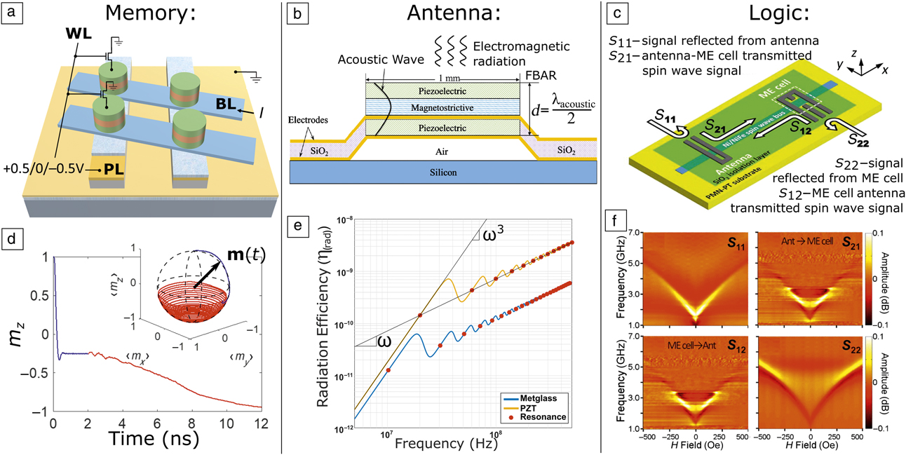
The large coupling strength and nonvolatility make strain-mediated ME control ideal for memory applications.Reference D’Souza, Fashami, Bandyopadhyay and Atulasimha30,Reference Sohn, Nowakowski, Liang, Hockel, Wetzlar, Keller, McLellan, Marcus, Doran, Young, Kläui, Carman, Bokor and Candler32,Reference Lo Conte, Xiao, Chen, Stan, Gorchon, El-Ghazaly, Nowakowski, Sohn, Pattabi, Scholl, Tamura, Sepulveda, Carman, Candler and Bokor39,Reference Sohn, Liang, Nowakowski, Hwang, Han, Bokor, Carman and Candler48–Reference Wang, Li, Liang, Barra, Domann, Lynch, Sepulveda and Carman51 Figure 3a,d shows a recently proposed ME memory device and model by Wang et al., indicating ME control combined with spin orbit torque enables deterministic control of MRAM with nanosecond switching times.Reference Wang, Domann, Yu, Barra, Wang and Carman52 Additionally, D’Souza et al. calculated the energy to flip a single bit to be approximately 1 aJ, multiple orders of magnitude better than commercial devices.Reference D’Souza, Fashami, Bandyopadhyay and Atulasimha30 D’Souza explained how this could enable a device with 106 bits clocked at 1 GHz to dissipate as little as 100 μW.Reference D’Souza, Fashami, Bandyopadhyay and Atulasimha30 Such small power requirements can be met with modern energy harvestingReference Chu, Annapureddy, PourhosseiniAsl, Palneedi, Ryu and Dong53,Reference Mori and Priya54 to provide a new paradigm in autonomous electronics systems (e.g., for the Internet of ThingsReference Leung, Or, Ho and Lee55 or implantable technologies). At a large scale, memory this efficient can cut into the 70 billion kWhr of energy used by United States data centers every year (i.e., 1.8% of the total US energy expenditure).Reference Shehabi, Smith, Sartor, Brown, Herrlin, Koomey, Masanet, Horner, Azevedo and Lintner56
Examples of strain-mediated magnetoelectric (ME) coupling controlling the (a) storage, (b) transmission, and (c) processing of information. Each device has the potential for order of magnitude improvements in energy efficiency or size, over current state-of-the-art technologies. (a, d) Schematic and modeled response, respectively, of ME memory. (d) Blue line indicates voltage (strain) is applied, while red line indicates relaxation after the voltage is removed. Deterministic 180° rotation is predicted (i.e., flipping a 0 to a 1). (b) Schematic of a film bulk acoustic resonator (FBAR) ME antenna. (e) Radiation efficiency for acoustically driven magnetoelastic (Metglas) and piezoelectric (PZT) antennas. These effects are combined in a ME antenna. (c) Schematic of ME spin wave bus (cell) for constructing logic gates, and (f) measured S-parameters. (c, e, f) Reprinted with permission from References Reference Cherepov, Amiri, Alzate, Wong, Lewis, Upadhyaya, Nath, Bao, Bur, Wu, Carman, Khitun and Wang45 and Reference Domann and Carman57. © 2014 and 2017 AIP publishing. (b) Reprinted with permission from Reference Reference Yao, Wang, Keller and Carman58. © 2015 IEEE. Note: WL, word line; BL, bit line; PL, plate line; I, current; λacoustic, acoustic wavelength; ω, angular frequency; Ant., antenna; PZT, Pb(ZrxTi1–x)O3; H, magnetic field; m x, m y, and m z, magnetization unit vectors in x, y, and z directions, respectively; m, magnetization unit vector; t, time.

Transmission: Miniature antennas and radio frequency devices
Several authors have proposed ME antennas to transmit and receive information.Reference Domann and Carman57–Reference Keller, Sepulveda and Carman63 Figure 3b shows a proposed bulk acoustic wave antenna,Reference Yao, Wang, Keller and Carman58 and Figure 3e shows theoretical radiation efficiency predictions.Reference Domann and Carman57 In addition to antennas, numerous strain-mediated radio frequency (RF) components from tunable inductorsReference Wu and Carman43 to filters and phase shiftersReference Yang, Sun, Srinivasan, Priya and Sun64,Reference Lou, Liu, Reed, Ren and Sun65 have been developed. A primary motivation for ME RF devices is to reduce the size of modern components using the ∼5 order-of-magnitude wavelength reduction when an electromagnetic wave is converted into an acoustic wave. Strong ME coupling and low loss could enable revolutionary chip-scale antennas, RF gyrators, and isolators for full-duplex radios. The latter two devices rely on controlling nonreciprocal wave propagation, so waves (i.e., information signals) traveling in opposite directions can be effectively separated from one another. In addition to size advantages, magnetic antennas are better than electric antennas for transmitting in lossy environments due to a predominantly magnetic near-field.Reference Manteghi and Ibraheem66 If these technologies are successful, the size of our communications technology could be reduced by several orders of magnitude and allow for transmission from challenging locations (e.g., underground, under water, or to/from implanted diagnostics and therapeutics inside the human body).
Processing: Spin wave logic devices
Spin wave logic devices (e.g., XNOR gates) are being actively developed to allow spin-based processing to replace electron-based systems.Reference Bao, Zhu, Wong, Hockel, Lewis, Zhao, Wu, Amiri and Wang44,Reference Cherepov, Amiri, Alzate, Wong, Lewis, Upadhyaya, Nath, Bao, Bur, Wu, Carman, Khitun and Wang45,Reference Chen, Barra, Mal, Carman and Sepulveda67–Reference Schneider, Serga, Leven, Hillebrands, Stamps and Kostylev69 Figure 3c shows a key logic gate element, an ME spin bus.Reference Cherepov, Amiri, Alzate, Wong, Lewis, Upadhyaya, Nath, Bao, Bur, Wu, Carman, Khitun and Wang45 A coupled acoustic-spin wave is generated by one of the electrodes on this device and propagates to a detector on the far side. The surface plots in Figure 3f show the measured S-parameters (i.e., reflection and transmission properties). Logic gates combine multiple spin buses to constructively or destructively interfere these waves. The resulting high or low signal represents the 1 or 0 state, respectively, of the gate. The main goal with spin-based logic is to move away from inefficient transistor-based devices with large standby power that consume a sizeable fraction of the total energy.Reference Salehi and DeMara70,Reference Nikonov and Young71 Strain-mediated ME logic gates work analogously to purely magnetic spin wave logic,Reference Kostylev, Serga, Schneider, Leven and Hillebrands68,Reference Schneider, Serga, Leven, Hillebrands, Stamps and Kostylev69 however they can provide better energy efficiency, and the waves travel much longer distances before appreciable energy loss occurs.Reference Chen, Barra, Mal, Carman and Sepulveda67 Nikonov et al. found that ME devices have roughly three orders of magnitude smaller standby power, and one to two orders of magnitude smaller active power than almost any other existing technology.Reference Nikonov and Young71
On the horizon
Strain-mediated ME technologies have developed at a rapid pace during the past 17 years and are not slowing. While this article focused on examples controlling ferro-/ferrimagnetic materials, recent work has measured the strain-mediated control of exchange biased antiferromagnetic (AFM) materials.Reference Domann, Sun, Schelhas and Carman72,Reference Xue, Zhou, Peng, Zhu, Zhang, Ren, Ren, Yang, Nan, Sun and Liu73 AFM materials could be used in robust magnetic field-insensitive devices, but the same property that enables robustness makes them difficult to control with conventional field-based approaches, even at low frequencies. ME AFM control should show the same energy efficiency seen with ferromagnetic materials, and recent modeling efforts have even predicted that ME AFM control could lead to domain switching at near THz frequencies.Reference Barra, Domann, Kim and Carman74 This suggests ME coupling could control dynamic regimes and materials not feasible with most other technologies.
This article has illustrated how ME coupling provides orders of magnitude improvements in energy efficiency for data manipulation tasks, all while being fast and smaller than conventional technologies. It should be evident from the discussion that the types of improvements being made are not incremental in nature, but order of magnitude changes that open pathways to a paradigm shift in how we store, transmit, and process information.
Acknowledgments
This work was supported by the NSF Nanosystems Engineering Research Center for Translational Applications of Nanoscale Multiferroic Systems Cooperative Agreement Award (No. EEC-1160504), DARPA AMEBA Program: A Mechanically Based Antenna (No. HR0011-17-C-0117), the University Center of Excellence: High-Rate Deformation Physics of Heterogeneous Materials (BAA-AFOSR 2011-16), the Shanghai Pujiang Program (No. 18PJ1408300), and the Taiwan Ministry of Science and Technology (Grant No. 105-2628-E-009-001-MY2).

John Domann is an assistant professor in the Department of Biomedical Engineering and Mechanics at Virginia Tech. He received his BS and MS degrees from the University of Kansas in mechanical and bioengineering, and his PhD degree in mechanical engineering from the University of California, Los Angeles. He was previously a Fellow with the Institute for Advancing Medical Innovation researching smart orthopedic biomaterials and implants. His recent research has focused on magnetoelectric/multiferroic control to transmit information, and the response of magnetoelastic materials to impact and shock wave loading. Domann can be reached by email at jpdomann@vt.edu.

Tao Wu is an assistant professor at ShanghaiTech University, China. He received his BS degree from the Zhejiang University, China, in 2007, and earned his MS and PhD degrees from the University of California, Los Angeles, in 2009 and 2011, respectively. After graduation, he worked at Intel Corporation From 2014 to 2015, he was a postdoctoral researcher at Stanford University, leading a Google ATAP-funded monocentric imager project. He was a postdoctoral researcher in Northeastern University, leading a DARPA-funded Near-Zero sensor project. His research interests include novel multiferroic materials and transducers, micro-/nanoelectromechanical systems, micro-/nanomanufacturing, and advanced semiconductor processing. He has published numerous papers and has more than 1000 citations and an H-index of 16 (Google Scholar). Wu can be reached by email at wutao@shanghaitech.edu.cn.

Tien-Kan Chung is an associate professor in the Department of Mechanical Engineering at National Chiao Tung University (NCTU), Taiwan. He earned his PhD degree in mechanical engineering at the University of California, Los Angeles, in 2009. From 2009 to 2011, he worked in the Microelectromechanical Systems R&D Department at the Taiwan Semiconductor Manufacturing Company. Since 2011, he has been a faculty member at NCTU. His research interests include magnetic/piezoelectric sensors, actuators, energy harvesters, microelectromechanical systems, and nano-magnetoelectrics for medical, power-system, smart-manufacturing, and Internet of Things applications. Chung can be reached by email at tkchung@nctu.edu.tw.

Gregory P. Carman is the director of the National Science Foundation Engineering Research Center Translational Applications of Nanoscale Multiferroic Material Systems, and is Co-executive Director of the Center for Advanced Surgical and Interventional Technology in the Department of Surgery at the University of California, Los Angeles (UCLA). He joined the Mechanical and Aerospace Engineering Department at UCLA in 1991. He has served as chairman for the Adaptive Structures and Material Systems of the ASME (2000–2002), and is an associate editor for the Journal of Intelligent Material Systems, and Structures and Smart Materials and Structures. He was awarded the Northrop Grumman Young Faculty Award in 1995 and three best paper awards from the ASME in 1996, 2001, and 2007. In 2015, SPIE honored him with the SSM Lifetime Achievement Award, and in 2016, he was invited to be the Distinguished Lecturer for the IEEE Magnetic Society. His research interests focus on analytical modeling, fabrication, and testing of magnetoelectric materials and developing devices for medical applications. Carman can be reached by email at carman@seas.ucla.edu.