I. INTRODUCTION
Recently the application of radio frequency identification (RFID) is highly developed, especially the passive tags which are applicable in the field of science, commercial, and military. The tag circuit includes analog, digital, and memory parts. The analog part consists of rectifier, regulator, oscillator, modulator, and demodulator blocks. By increasing the distance between the tag and reader, the received power of the RFID tag is decreased. Therefore the designed blocks of the tag should have low-power dissipation to increase reading range.
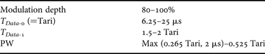
The radio frequency (RF) signal sent from the reader is detected by the demodulator block and after that they are digitized and are transmitted to the digital part. Based on electronic product code class1 generation2 (EPC C1 G2) protocol [1], in order to attenuate the power dissipation of the detector, the amplitude shift keying pulse interval encoding (ASK-PIE) demodulation is used for data transmission to the tag. In ASK modulation, data bits are sent as the short gaps in the RF signal. The ASK modulation depth is in the range of 80–100%. The PIE modulation causes the difference between data-0 and -1 pulse width (PW). In this modulation data-0 and -1 are determined based on the duration of positive voltage PW. In this case, the level of positive voltage is separated with each other with the short gaps named PW [Reference Ashry, Sharaf and Ibrahim2]. Table 1 presents the characteristics of data parameters sent from the reader based on EPC C1 G2 protocol.
The characteristics of data parameters sent from the reader based on EPC C1 G2 protocol [1].

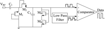
The data sent from the reader is detected by the demodulator block of the tag. In the RFID system, the data are transmitted to the tag as short gaps in the RF signal. Therefore, the simple envelope detector is used in the demodulator structure for detecting the gaps. The schematic diagram of the common ASK demodulator consisting of the envelope detector and digital part is shown in Fig. 1 [1].
Schematic diagram of the conventional demodulator.

The detector, which is the one-stage rectifier, connects to the RC circuit, M R1 and M R2 transistors act as resistor in the RC circuit. The average envelope of signal is calculated by passing through the low-pass filter (LPF). While RC circuit filters the RF carrier, it should have enough bandwidth to save the data sent from the reader. In other words, the multiplication of R and C should fulfill the condition of equation (1).
 $$\displaystyle{1 \over {2\pi f_{RF}}} \le RC \le \displaystyle{1 \over {2\pi f_{data}}},$$
where f RF and f data are the frequency of carrier wave and digital data rate, respectively. The values of R and C of equation (1) are achieved from equations (2) and (3), respectively.
 $$R = \left[ {\,\displaystyle{1 \over {g_{m,M_{R1}}}} + \,r_{d,M_{R2}}} \right] \vert \vert \,\left[ {\displaystyle{1 \over {g_{m,M2}}} + \displaystyle{1 \over {g_{m,M1}}}} \right]\,\,,$$
 $$\eqalign{C & = \displaystyle{{(C_1 + C_{gs,M1} + C_{ds,M1} )(C_{gs,M2} + C_{ds,M2} )} \over {(C_1 + C_{gs,M1} + C_{ds,M1} ) + (C_{gs,M2} + C_{ds,M2} )}} \cr & \quad+ \displaystyle{{C_{ds,M_{R2}} (C_{gs,M_{R1}} + C_{ds,M_{R1}} + C_{gd,M_{R2}} )} \over {C_{ds,M_{R2}} + (C_{gs,M_{R1}} + C_{ds,M_{R1}} + C_{gd,M_{R2}} )}} + C_2,}$$
where
 $r_{d,M_{R2}} $
is the drain–source resistor of M
R2 transistor, g
m
is the transconductance of transistors, C
gs
is the gate-source capacitor, and C
gd
is the gate-drain capacitor of transistors. Finally, the signal envelope and its average are employed to the comparator to do the comparison and the digital data with the appropriate voltage level is provided for the digital part.
The LPF stage doesn't operate well under different data rate, so it can't produce the signal with half of the signal envelope amplitude and consequently the data are detected with error in the demodulator shown in Fig. 1. One of the important parameters that should be noted in the designing is the selection of threshold voltage level for the comparison with the signal envelope in the comparator stage. Since by increasing the distance between the tag and reader, the available power to the tag is reduced, distinguishing the voltage level of 0 and 1 logic data becomes difficult. In this condition, if the threshold voltage level is changed related to the distance between the tag and reader, the accuracy in data detection is improved. In [Reference Ashry, Sharaf and Ibrahim2] the signal envelope is consistently compared with the fixed voltage which causes difficulty in the data detection in low voltages of RF input signal. The LPF stage in [Reference Najafi, Mohammadi, Roostaie and Fotowat-Ahmady3, Reference Pelissier4] includes RC circuit which has the drawback of large resistor and capacitor for decreasing the rapid variation of envelope voltage. The RC circuit in [Reference Yeager, Zhang, Zarrasvand, George, Daniel and Otis5] consists of weighted resistors which culminate in high chip area.
In this paper, the ASK demodulator is designed. The demodulator produces the suitable threshold voltage level related to the RF input signal with the help of average detector and voltage divider circuit. Therefore the accuracy of the data detection is increased even in long distance between the tag and reader. In addition, by using the small value of resistor and capacitor in the proposed circuit, the chip area is more reduced in comparison with similar circuits. To decrease the power consumption, only one enable input is used for the comparator and buffer circuits. The paper is organized as follows: the proposed demodulator is studied in Section II, the simulation results are presented in Section III, and finally the whole work is concluded in Section IV.
II. THE PROPOSED ASK DEMODULATOR
Usually the ASK demodulator block is directly connected to the tag antenna. Fig. 2 illustrates the block diagram of the proposed ASK demodulator. The demodulator consists of the voltage multiplier, envelope detector, voltage divider, average detector, comparator, and inverter.
Block diagram of the proposed ASK demodulator.

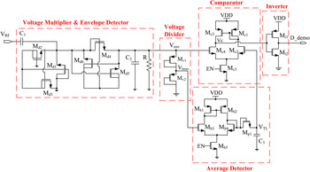
The voltage divider and the average detector generate the threshold voltage level (V TL ) which is changed by the variation of the RF input signal. Therefore the signal envelope is compared with the threshold voltage level produced based on the input signal. In this case, more accuracy in the data detecting is achieved. Fig. 3 indicates the proposed circuit schematic.
The proposed ASK demodulator.

A) Voltage multiplier and envelope detector
The multiplier circuit, which rectifies the RF input signal, is the Dickson voltage doubler circuit including M d1–M d6 transistors. M d2–M d3, and M d5–M d6 transistors, respectively, connect the body of M d1 and M d4 pass transistors to the minimum voltage. Thus by reducing the loss of body effect, the increasing of M d1 and M d4 threshold voltage is prevented. The next stage is the envelope detector which includes the resistor R and the capacitor C 2. This circuit extracts the data envelope by omitting the carrier wave.
Since the mobility of the electrons is larger than that of holes, the speed of n-channel metal—oxide—semiconductor (NMOS) transistors is more than that of p-channel metal—oxide—semiconductor (PMOS) transistors and also the chip area of the NMOS transistors is smaller than that of PMOS for the specific drain current. Therefore in design of voltage multiplier and envelope detector NMOS transistors are used.
If the carrier of the input signal equals to V = V a cosωt, in the negative cycle M d1 and M d4 transistors work in saturation and cut-off region, respectively, and in the positive cycle the working regions become reversed. In each cycle, the transistor is not completely off; as a matter of fact it conducts the reverse leakage current. Therefore the transistor works in sub-threshold region.
If the produced charges from the source in one period are considered as ΔQ in and the total charges of load and the leakage current of transistor in sub-threshold region are considered as ΔQ out , then ΔQ in = ΔQ out based on the charge conservation equation. When M d1 transistor works in saturation region and for the first stage of Dickson circuit ΔQ in is calculated as equation (4). Using the Taylor series of cosωt, ΔQ in is achieved as equation (5) [Reference Yi, Ki and Tsui6].
 $$\eqalign{\Delta Q_{in} & = \,\Delta Q_{sat} = \int {\,\displaystyle{1 \over 2}} \,\,\mu _n \,C_{ox} \left( {\displaystyle{W \over L}} \right)\,(V_{gs} \, - V_{tn} )^2 \,dt \cr & = \int {\,\displaystyle{1 \over 2}} \,\,\mu _n \,C_{ox} \left( {\displaystyle{W \over L}} \right)\,\left[ {V_a \,\cos \omega t\, - \overline V _o - V_{tn}} \right]^2 dt}$$
 $$\Delta Q_{in} = \displaystyle{{8\,T\,\mu _n \,C_{ox} \,\left( {W/L} \right)} \over {15\,\pi \,\sqrt {2\,V_a}}} \,(V_a - V_{tn} - \overline V _o )^{5/2}$$
where
 $\overline V _o $
is the output voltage average of Dickson first stage and (W/L) is ratio of width to length of M
d1 transistor. μ
n
, Vtn, Cox
, and T are the electron mobility, the threshold voltage of NMOS transistor, the capacitor of gate oxide and the period of carrier wave, respectively.
In the next cycle M d1 works in sub-threshold region, in fact the source and drain terminal of M d1 are interchanged. Therefore V gs of M d1 transistor equals to zero and V ds is defined as equation (6).
 $$V_{ds} = \overline V _o \, - \,V_a \,{\rm cos}\omega t.$$
Therefore ΔQ out is calculated based on equation (7) that by considering the Taylor series of cosωt equation (7) is obtained [Reference Yi, Ki and Tsui6].
 $$\eqalign{\Delta Q_{out} & = \Delta Q_{Load} \, + \,\Delta Q_{Leak} \, = \,I_{Load} T\, \cr & \quad+ \,\int {\,I_{o,n} \,\left( {\displaystyle{W \over L}} \right)\,\left( {1 - \,\,exp\left( {\displaystyle{{ - V_{ds}} \over {V_T}}} \right)} \right)\,dt}},$$
 $$\Delta Q_{out} = \,I_{Load} \,T\, + \,I_{o,n} \,\displaystyle{W \over L}\,\left( {1 - \,exp\,\left( {\displaystyle{{V_a} \over {V_T}}} \right)} \right),$$
 $$I_{o,n} = \,\mu _n \,\sqrt {\displaystyle{{q\,\varepsilon _{si} \,N_{ch}} \over {2\,\varphi _s}}} \,V_T^2 \,exp\left( { - \displaystyle{{\left( {V_{tn\,} + \,V_{off}} \right)} \over {nV_T}}} \right),$$
where V T is the thermal voltage, I Load is the load current, and I o,n of NMOS transistor is defined as equation (9).
where ε si is the silicon permittivity, N ch is the doping concentration in the channel, Φ s is the surface potential, V off is the sub-threshold region offset voltage and n is the sub-threshold region swing parameter. Based on the charge conservation theorem and the equality of equations (5) and (8) the average of output voltage from the Dickson first stage is calculated as equation (10).
 $$\overline V _o = \,\,\left[ {V_a - V_{tn} \, - \left( {\displaystyle{{15\,\pi} \over 8}\,\displaystyle{{I_{oeff} \,\sqrt {2\,V_a}} \over {\mu _n \,C_{ox} \left( {W/L} \right)}}} \right)^{{2 / 5}}} \right],$$
where I oeff is the effective loading current and includes the load and leakage currents of the transistor in the sub-threshold region. It is defined as equation (11).
 $$I_{oeff} = \,I_{Load} + \,\displaystyle{{I_{o,n}} \over \pi} \,\,\displaystyle{W \over L}\,\,\left( {1 - exp\left( {\displaystyle{{ - V_a} \over {V_T}}} \right)} \right)\,\,.$$
The output voltage calculation of the second stage of Dickson circuit is similar to that of the first stage. Thus, V env is calculated as equation (12).
 $$V_{env} = \,2\,\left[ {V_a^{\prime} - V_{tn} \, - \left( {\displaystyle{{15\,\pi} \over 8}\,\displaystyle{{I_{oeff}^{\prime} \,\sqrt {2\,V_a^{\prime}}} \over {\mu _n \,C_{ox} \left( {W/L} \right)}}} \right)^{{2 / 5}}} \right],$$
where
 $I_{oeff}^{\prime}$
is the effective loading current at the
 $V_{a}^{\prime}$
voltage that can be calculated as equation (9) and
 $V_{a}^{\prime}$
is the effective voltage amplitude seen from the diode-connected transistor and it is defined as equation (13).
 $$V_a^{\prime} \, = \,\displaystyle{C \over {C + C_{par}}} \,V_a.$$
In the proposed circuit, the values of C 1 and C 2 capacitors are considered equal and stated as C, while C par is the parasitic capacitor of each node.
B) Voltage divider
The diode-connected transistors M v1 and M v2 working in the sub-threshold region form the voltage divider. Also M v1 and M v2 transistors have similar dimensions. Therefore, based on the Kirchhoff's law, V henv equals to half of the envelope signal voltage, V env .
Under the same conditions the PMOS transistors have larger resistor than NMOS transistors which leads to driving lower current from the prior stage (voltage multiplier and voltage divider). Therefore in the design of voltage divider, PMOS transistors are used.
C) Average detector and comparator
The average voltage detector consists of the buffer circuit, M p1 diode-connected transistor and C 3 capacitor. M b1–M b5 transistors of differential buffer which has the unit gain isolate the output voltage of the demodulator from the source-gate capacitor of the voltage divider. In addition, M p1 transistor prevents the reversed current. M p1 transistor and C 3 capacitor organize the LPF, thus V TL equals to the average voltage which is employed to the drain of M p1 transistor.
V henv is the square function, M p1 transistor and C 3 capacitor work as integrator circuit. Since the length and width of M p1 are small the drain-source and gate-source capacitors are neglected in comparison with C 3. Thus V TL is calculated versus time based on equation (14).
 $$V_{TL} (t) = V_{henv} \left( {1 - exp{\kern 1pt} \left( { - \displaystyle{{g_{m,Mp1} t} \over {C_3}}} \right)} \right) + V_C {\kern 1pt} exp{\kern 1pt} \left( { - \displaystyle{{g_{m,Mp1} t} \over {C_3}}} \right),$$
where g m, Mp1 is the transconductance of Mp1 and V c is the primary voltage of the circuit. In this case, the average of V TL (t) is calculated based on equation (15).
 $$\eqalign{{V_{TL}} & = \displaystyle{1 \over T} \left[\int_T \left( V_{henv} \left( {1 - exp \left( { - \displaystyle{{g_{m,Mp1} t} \over {C_3}}} \right)} \right) \right.\right. \cr & \quad \left.\left. + V_C exp\,\left( { - \displaystyle{{g_{m,Mp1} t} \over {C_3}}} \right)\right) dt \right],}$$
where T is the period of sent data. Due to equations (14) and (15) V TL depends on V henv at any time and also V henv is related to the amplitude of sent signal from the reader. In other words by changing the amplitude of input RF signal the value of threshold voltage is changed.
Then V env and V TL voltages are employed to the negative and positive comparator terminals, respectively, and finally the comparator output is employed to the inverter in order to generate the logic data with the appropriate voltage level for the digital part.
The differential voltage gain depends on the load connected to the drains of differential pair transistors. Therefore, in this paper, the active load is employed for improving the differential voltage gain. Since the PMOS transistors have larger resistors than NMOS transistors under the same condition and the voltage of current mirror source has the closer value to supply voltage (VDD) and the PMOS transistor passes the VDD voltage level, in the design of current mirror source which is employed to the comparator and average detector circuit PMOS transistor is used. In the inverter both PMOS and NMOS transistors are used for increasing the voltage swing. Because PMOS transistor passes VDD perfectly while NMOS transistor passes ground (GND) voltages.
For reducing the power dissipation one enable input enable (EN) is used for both the buffer and comparator circuit. In this case, during the transmitting data with backscatter modulation from the tag to the reader and when there is no requirement to the data detection, the buffer and comparator don't dissipate the power.
III. SIMULATION RESULTS
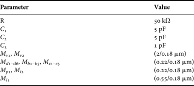
The proposed demodulator is simulated in 0.18 µm complementary metal–oxide–semiconductor (CMOS) technology with the Cadence software. The input of the demodulator is the 10-bit string. The values of transistors sizes, resistors, and capacitors are presented in Table 2. The values of resistors and capacitors of the proposed demodulator are significantly decreased which culminates in the reduction of the chip area.
The transistors sizes and the values of resistors and capacitors of the demodulator.

The bandwidth of the envelope detector is 4 MHz which fulfills the condition of equation (1). Also R resistor cannot be replaced with diode-connected transistor, because the transistor needs high current in range of micro-ampere to create the resistor in the range of kilo-ohm.
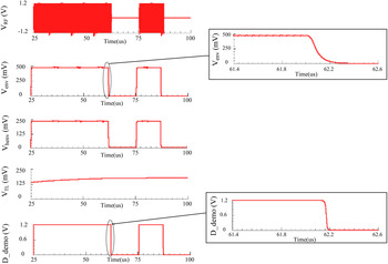
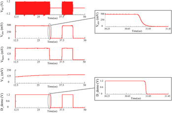
Figure 4 indicates the different nodes waveform of the proposed circuit under the condition of 40 KHz data rate and 100% modulation depth at 960 MHz carrier frequency and 1.2 V supply voltage. Using the inverter circuit the suitable output voltage of the demodulator is provided for the processing in the digital part. Figure 5 shows the waveform of the various circuit nodes with 80 KHz data rate and 100% modulation depth at 1.2 V supply voltage. The simulation results show that the demodulator works properly and has the appropriate performance for two different data rates.
Waveform of different circuit nodes at 40 kHz data rate.

Waveform of different circuit nodes at 80 kHz data rate.

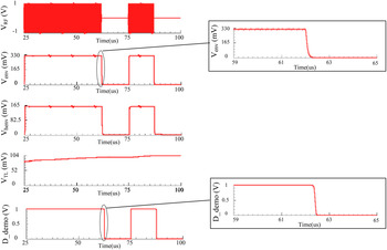
Since V TL is adjusted based on the RF input signal, the comparison between the envelope signal and the threshold voltage is done more accurately and the error of data detection is decreased. Figure 6 shows the different nodes waveform of the proposed demodulator with 40 KHz data rate at 1 V supply voltage.
Waveform of different circuit nodes at 40 kHz data rate and 1 V supply voltage.

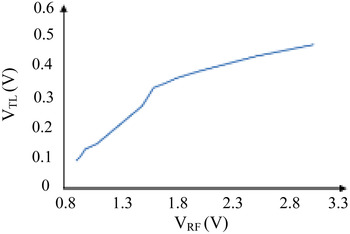
For evaluating the performance of the proposed circuit in the various input voltages the variations of threshold voltage (V TL ) related to the variations of RF input signal amplitude is presented in Fig. 7.
Variations of threshold voltage (V TL ) versus the amplitude of RF input signal.

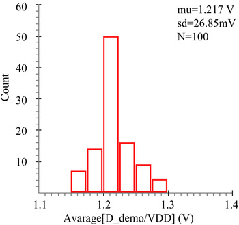
The impact of mismatch and process variation on the average ratio of D_demo voltage to VDD is shown in Fig. 8 by 100 runs of Monte Carlo simulation in which the mean and the standard deviation lie around 1.217 and 26.85 mV, respectively.
Impact of mismatch and process variation on average of ratio of D_demo voltage to VDD.

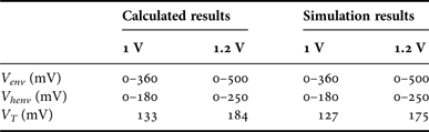
The obtained equations are calculated by the numerical method. The comparison between the calculated results and the results of Cadence simulation at 1 and 1.2 V supply voltage is shown in Table 3. The results of Cadence simulation show good agreement with the calculated results.
The comparison between the calculated results and results of Cadence simulation.

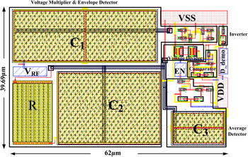
The layout of the proposed demodulator is shown in Fig. 9 which consumes 0.0025 mm2 chip area and dissipates 3.9 nW power.
Layout of the proposed demodulator.

Table 4 compares the proposed demodulator with the other ASK demodulator as the demodulator dissipates the lower power.
The comparison of the proposed demodulator with the other ASK demodulator.

IV. CONCLUSION
In this paper, the ASK demodulator with 100% modulation depth is proposed for the RFID passive tags working at 960 MHz frequency. In this circuit, the suitable threshold voltage level changed by the variation of the RF input signal is produced by using the buffer and average detector. Therefore the detection accuracy is increased even at the low voltages. The sizes of the employed resistor and capacitor are very small and for decreasing the power consumption one enable input EN is used for both the buffer and comparator circuits. The simulation is done in 0.18 µm CMOS technology at 1.2 V supply voltage and it indicates that the chip area and the power consumption of the proposed demodulator are 0.0025 mm2 and 3.9 nW, respectively. The demodulator has the proper operation for 40 and 80 KHz data rates.
 Rezvan Dastanian was born in Iran, Ahvaz, in 1986. She received her B.Sc. and M.Sc. degrees in Electrical Engineering from Iran University of Science and Technology (IUST), Iran, Tehran in 2008 and 2011, respectively, and her Ph.D. degree in Electronic Engineering at Shiraz University of Technology (SUTECH) in 2015. She has been with the Imam Hussein Faculty of Engineering, Behbahan Khatam Alanbia University of Technology, since 2015. Her research interests include RFIC design, low-power circuit design, and microelectronics.
 Ebrahim Abiri received his B.Sc. degree in Electronics Engineering from Iran University of Science and Technology (IUST) in 1992, M.Sc. degree from Shiraz University in 1996, and the Ph.D. degree in Electronics from IUST in 2007. He has authored more than 50 published technical papers in electronics and power electronics and four books. He has been with the Department of Electrical Engineering, Shiraz University of Technology (SUTECH), since 2007. His current research activities include analog circuit design and power electronic.
 Khadije Taherinia was born in Iran, Bushehr, in 1990. She received her B.Sc. and M.Sc. degrees in Electrical Engineering from Shiraz University of Technology (SUTECH) in 2012 and 2015, respectively. Her research interests include RFID and low-power circuit design.