Introduction
The chipless RFID tags [Reference Rezaiesarlak and Chipless1–Reference Subrahmannian and Behera4] are gaining popularity due to their lower environmental impacts during production and disposal, and their advantages, such as robustness, durability, cost effectiveness, and flexibility in integration, make them superior to the traditional RFID tags with integrated chips. Additionally, the chipless RFID tags have higher security features as they are less vulnerable to hacking and cloning compared to other types of microchip embedded tags. These tags operate on the electromagnetic backscattering principle [Reference Herrojo, Paredes, Mata-Contreras and Martín5] and make use of their unique physical structure to encode and reflect the information when interrogated by an RFID reader. The tags are printed on the thin dielectric substrate, and the printed resonator patterns on the substrate store the data physically. Among various encoding techniques, such as frequency domain, time domain, or amplitude/phase/polarization, the frequency domain encoding is the simplest to implement. The RFID reader emits the electromagnetic signal and reads the modified reflections coming from the tag. Recently, there was a great deal of interest in the RFID-based sensor [Reference Karmakar, Amin and Saha6–Reference Ahmadihaji, Izquierdo and Shih8] design for sensing various physical parameters.
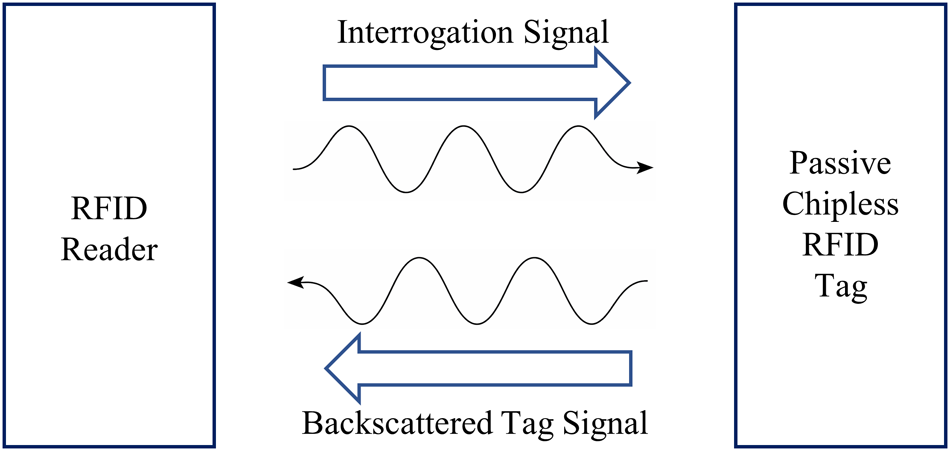
Figure 1 illustrates the fundamental operating mechanism of a passive chipless RFID system [Reference Dey, Bhattacharyya, Sarma and Karmakar9, Reference Mishra, Das, Behera and Karmakar10]. The RFID reader initiates the communication by transmitting a continuous-wave (interrogation signal) toward the passive chipless RFID tag. This incident electromagnetic wave illuminates the tag and excites its resonant elements. The chipless RFID tag does not contain any active components or internal power source. Instead, it encodes information through its physical structure, which selectively alters the amplitude, phase, or frequency characteristics of the incident signal. As a result, the tag reflects the incident wave back toward the reader in the form of a backscattered tag signal carrying a unique electromagnetic signature. The RFID reader receives this backscattered signal and processes it to extract the encoded information associated with the tag. This backscatter-based communication enables low-cost, maintenance-free identification without the need for integrated circuits or batteries.
Basic working block diagram of a passive chipless RFID tag.

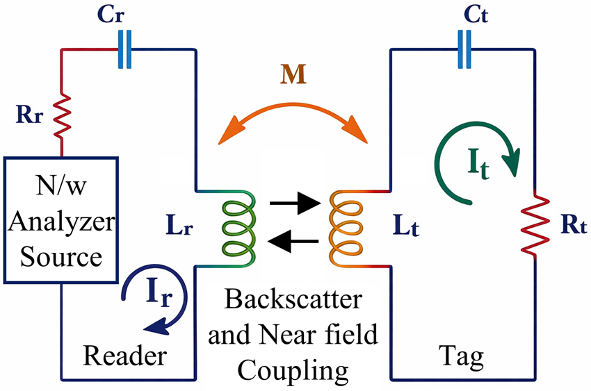
A generalized equivalent circuit model of the chipless RFID system is shown in Figure 2 [Reference Mishra, Das, Behera and Karmakar10]. The reader is excited by a vector network analyzer acting as the signal source, while the passive tag is energized through electromagnetic coupling from the reader. Both the reader and the tag are represented by equivalent resistance  $(R)$, capacitance
 $(C)$, and inductance
 $(L)$ elements that describe their resonant characteristics. Where
 $I_r$ and
 $I_t$ represent the equivalent current amplitudes associated with the reader and the tag, respectively. The interaction between the two circuits occurs through a combination of near-field coupling and backscattered signal radiation, which enables wireless power transfer and information encoding in the chipless RFID system.
Basic equivalent circuit diagram of a passive chipless RFID tag system [Reference Mishra, Das, Behera and Karmakar10].

Design of RFID tags for wearable applications [Reference Behera11] faces several challenges. First, the high dielectric constant and lossy nature of the body absorb the RF signal, raising the issue of electromagnetic compatibility in terms of specific absorption ratio (SAR). Electromagnetic coupling between the tags also deteriorates the accuracy of the measurement due to the cross-sensitivity [Reference Meng and Li7]. Additionally, it also leads to detuning of the antenna impacting in a reduction in gain and lowering of the read range. Flexibility and conformability are also challenging for wearable applications since physical deformation may change the shape of the radiating element, leading to impedance mismatch and detuning of the antenna. Therefore, the use of a thin, flexible substrate is the preferred choice for wearable applications. Furthermore, the compactness and overall size of the tag antenna are one of the most important requirements for wearable applications, which may lead to lower efficiency and read range. Additionally, the availability of a stable power source for wearables limits the use of active or semi-passive tags; therefore, the passive RFID tags are found to be most suitable for such applications. However, passive RFID tags have a limited reading range that needs to be improved. Gain of the transmitting and receiving antennas, the reader transmitted and received power, and the tag’s radar cross section (RCS) and the wavelength [Reference El-Hadidy, El-Awamry, Fawky, Khaliel and Kaiser12] play an important role in improving the read range. A single-cell configuration of the RFID tag has limited RCS, hence limited read range. Therefore, to increase the RCS and the read range, the size of the reflecting area of the tag needs to be increased. Placing the RFID tags in an array configuration increases the RCS [Reference El-Hadidy, Lasantha, Khan, Sayed and Karmakar13, Reference Polivka, Svanda and Machac14] and hence the read range [Reference Anee and Karmakar15–Reference Kaur, Agarwal and Khanna17]. However, for wearable applications [Reference Behera11, Reference Corchia, Monti and Tarricone18], mutual coupling between elements of the tag antenna array [Reference Asl, Ghasr, Zawodniok and Robinson19–Reference Wang, Xu, Ye, Huang, Wang and Xiao22] is a major concern due to the requirement of compactness and body proximity. It is to be noted that the coupling detunes resonant frequencies, alters the input impedance of each element, and gives rise to reduced directivity due to weakening of constructive interference, and thereby deteriorates the performance of the array that eventually reduces the reading range of the tag [Reference Machac and Polivka23]. There are several techniques to reduce the mutual coupling between the array elements [Reference Wang, Xu, Ye, Huang, Wang and Xiao22–Reference Yang and Rahmat-Samii25]. Increasing the inter-element spacing is the easiest approach to reduce coupling. Use of some decoupling structures [Reference Gao, Cao, Fu, Quan and Chen26–Reference Tan, Wang, Wu, Liu and Kishk29] (Electromagnetic bandgap structures, defected ground structures, etc.), addition of isolation stubs or neutralization lines, or optimizing feed network and array layout are other commonly used techniques for reducing the mutual coupling among elements of patch antenna array configurations. Nevertheless, due to the issue of compactness, most of these techniques are not suited for wearable applications. Another feasible technique for controlling the electromagnetic coupling between the tag elements is based on the selection of the specific structure of the radiating element, optimization of its physical dimension by adjusting the lengths, widths, and, most importantly, the orientations of the tag element. In the proposed work, by orienting the folded split ring gap appropriately, the coupling between the tags is minimized without compromising on the compactness while maintaining only small gaps between the elements. Both inbound and outbound interferences are analyzed. Since the tag elements are receiving signal externally from the reader, both in-band and out-of-band interferences can be treated as in-band and out-of-band interferences, respectively. It is to be noted that the issue of coupling between the elements of the passive RFID tag array has received little attention so far.
The subsequent sections of this paper are organized as follows. Section II presents the design methodology of the wearable tag array, including configurations with single, two, and four elements. Section III provides a detailed parametric analysis along with surface current distribution and SAR evaluation. The experimental validation and measured results of the proposed tag array are discussed in Section IV. Finally, Section V concludes the work with key findings and observations.
Design of a wearable chipless RFID tag
In this section, the design of a star-shaped passive chipless RFID tag (SPRT) array printed on a flexible polyimide substrate for wearable applications is presented. Polyimide is a widely used dielectric substrate in RF and wearable antenna designs due to its low dielectric loss, thin profile, and excellent flexibility [Reference Singh, Khan, Kumar, Kanaujia, Choi and Kim30, Reference Khattak, Ahmed, Shoaib, Lazaridis and Ahmed31]. It exhibits stable dielectric properties with low dissipation factors at high frequencies, allowing efficient signal propagation with minimal loss. Additionally, polyimide offers mechanical durability and conformability, which makes it suitable for integration with fabric or flexible wearable platforms. These characteristics collectively make polyimide a cost-effective and high-performance material for wearable applications. The proposed design explores electromagnetic coupling behavior under two distinct scenarios: one where all tag elements in the array are identical in size, and another where the array consists of elements with two different sizes. This dual approach enables a detailed investigation of both inbound and outbound electromagnetic interference (EMI) effects. Furthermore, the orientation of each tag element within the array is optimized to minimize inter-element coupling and enhance the read range, which is an essential factor for the efficient performance of passive RFID systems.
Single element tag
The proposed single-element RFID tag, illustrated in Figure 3, is constructed on a flexible polyimide substrate with dimensions of  $41~ mm \times 41~mm \times 0.125~mm$ (
 $l_1 \times w_1 \times h$). The substrate has a dielectric constant (
 $\epsilon_r$) of
 $3.5$ and a loss tangent (
 $tan\delta$) of
 $0.008$. The star-shaped geometry is designed by overlaying two equilateral triangles in opposite orientations. Each triangle originates from a circular base, where a circle of radius
 $'r'$ is geometrically transformed into an equilateral triangle. Considering the need for a compact and lightweight structure in wearable devices, the proposed design is chosen to reduce the physical size of the tag without compromising its functional performance. The distributed star-shaped structure enhances the effective aperture of the tag and ensures uniform distribution of current, contributing to improved resonance characteristics.
The proposed single-element SPRT. (a) Top view. (b) Side view. (c) Dimetric view.

Figure 3 Long description
The image consists of three parts labeled as (a), (b) and (c). In part (a), the top view of the single-element SPRT is shown. It features a star-shaped design with two overlaid equilateral triangles in opposite orientations, originating from a circular base. The dimensions are marked as l subscript 1 and w subscript 1, with additional parameters g, a, d and w indicated. Part b presents the side view, illustrating the layered structure with colors representing different materials: copper, polyimide, foam, skin layer 1, skin layer 2 and fat layer. Part c provides a dimetric view, showing the layered composition in a three-dimensional perspective. The layers are labeled with thicknesses h subscript 1, h subscript 2, h subscript 3, h subscript 4 and h subscript 5, corresponding to the materials listed in the legend. The coordinate axes x, y and z are also depicted, indicating the orientation of the structure.
To reduce the overall weight and enhance mechanical flexibility, the design utilizes a polyimide substrate in combination with a lightweight foam isolation layer. This foam layer ( $h_1$) is positioned beneath the substrate to maintain a consistent separation from the skin, thereby enhancing mechanical stability and ensuring accurate electromagnetic response. This foam layer minimizes the body-loading effect caused by the lossy and conductive nature of human tissue, which otherwise could detune the chipless RFID tag and degrade its performance. This configuration also helps in maintaining a stable resonance frequency, effective impedance matching, and a consistent radiation pattern. Moreover, the foam layer improves user comfort by adding softness and cushioning for prolonged wear. To emulate realistic wearable conditions, a three-layer human skin model is placed below the foam layer, as shown in Figure 3. The outermost skin layer (
 $h_2$) functions as a barrier against ultraviolet (UV) radiation and prevents moisture loss. The middle layer (
 $h_3$) contains biological components such as blood vessels, nerve endings, sweat glands, sebaceous glands, and hair follicles. The innermost layer (
 $h_4$) consists predominantly of subcutaneous fat tissue, serving as insulation and energy storage. A comprehensive set of optimized physical parameters used in designing the proposed single-element RFID tag (Figure 3) is presented in Table 1.
Design parameters for the proposed SPRT array

Table 1 Long description
The table lists geometric design parameters for an SPRT array, giving numeric values primarily in millimeters. Many length and width parameters are large and similar, with several set to 80 millimeters and others at 76, 79, or 41 millimeters. Two k parameters are close in size at 36 and 37 millimeters, while the corresponding uppercase K parameters differ more at 37 and 33 millimeters. Small-scale features include a height value of 0.125 millimeters and another as low as 0.05 millimeters, plus a copper thickness of 0.018 millimeters. Additional dimensions include a radius of 12 millimeters and a gap of 1 millimeter. The remaining small parameters are 0.75 millimeters for w, 1 millimeter for d and a, and 0.5 millimeters for s. Values are presented as fixed design inputs without ranges or uncertainty, so no variability or tolerance can be inferred.
*Where  $`t`$ is the thickness of the copper and values are in
 $`mm`$.
Two element tag array
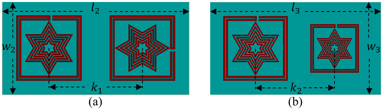
Figure 4a and b illustrate the inbound and outbound configurations of the proposed two-element RFID tag setup, respectively. This design investigates the electromagnetic coupling behavior under two specific scenarios: one in which both tag elements are identical in size, and another in which the two elements differ in size. These configurations are strategically chosen to analyze the influence of size variation on the EMI response in both inbound and outbound regions. In both configurations, the two tag elements are placed at a distance of  $k_1$ (
 $36~ mm$) and
 $k_2$ (
 $37~ mm$) from their center position, respectively, to study the near-field interaction and coupling characteristics. This setup provides valuable insights into the mutual coupling effects that can degrade system performance in dense tag environments, such as wearable or compact IoT applications. By altering the size and orientation of the tag elements (Figure 4), the design aims to achieve minimal inter-element coupling, leading to improved isolation and enhancing the tag read range for reliable operation in passive RFID systems.
The proposed two-element SPRT. (a) Inbound configuration. (b) Outbound configuration.

Four element tag array
The proposed four-element chipless RFID tag array is designed to further investigate electromagnetic coupling behavior in more complex tag configurations. As illustrated in Figure 5a, the inbound configuration is achieved by arranging the tag elements in a square formation with each tag rotated by  $90$ degrees relative to its neighbor at a distance of
 $K_1$ (
 $37~ mm$) from their center position. This rotational layout increases the likelihood of near-field interaction among elements, making it suitable for analyzing dense environments where mutual coupling effects are more pronounced. In contrast, the outbound configuration shown in Figure 5b positions the tag elements face-to-face by taking a two-element outbound configuration (Figure 4b) at a distance
 $K_2$ (
 $33~ mm$) from their center position, but with deliberate variation in size to suppress coupling and to compare the performance of the outbound configuration with the inbound configuration. Specifically, the secondary tag elements are reduced by 25% in size relative to the primary element. This scaling is performed to weaken the resonance overlap and limit mutual coupling between elements, ultimately enhancing the electromagnetic isolation. By comparing the performance of the four-element array in both configurations, the design aims to reveal critical insights into the relationship between element orientation, size mismatch, and EMI suppression. The optimized spatial arrangement and dimensional variation contribute to improved read range, more stable resonance behavior, and better isolation, especially in wearable or densely packed environments for the chipless RFID system. The dimensions used in the development of the proposed two and four-element RFID tag arrays, for inbound and outbound configurations, have been systematically optimized and are listed in Table 1.
The proposed four-element SPRT. (a) Inbound configuration. (b) Outbound configuration.

Figure 5 Long description
The image consists of two configurations of a four-element RFID tag array. On the left, labeled as (a), the inbound configuration displays four star-shaped elements arranged in a square formation. Each element is rotated by ninety degrees relative to its neighbor, with a distance labeled K subscript 1 between their centers. The dimensions L subscript 1 and W subscript 1 are marked along the edges of the square. On the right, labeled as (b), the outbound configuration shows the elements positioned face-to-face. The distance between the centers is labeled K subscript 2, with dimensions L subscript 2 and W subscript 2 marked. The secondary elements appear smaller than the primary ones, indicating a size variation in this configuration.
Parametric study of unit cell and array tag
This section presents a parametric analysis of the proposed RFID tag configurations to understand their electromagnetic behavior under various array arrangements. The study focuses on evaluating the reflection characteristics ( $|S_{11}|~ dB$) and surface current distributions of single, dual, and four-element tag structures in both inbound and outbound configurations. Key parameters such as inter-element spacing and tag orientation are varied to observe their effect on the coupling performance.
Reflection characteristics of single, dual, and four-element tag
Figure 6 presents the  $|S_{11}|~ dB$ versus frequency (
 $GHz$) plot of the proposed RFID tag under single, dual, and four-element configurations for both inbound and outbound arrangements. In the inbound configuration (Figure 6(a)), the single-element tag exhibits dual resonances at
 $3.76~ GHz$ and
 $3.96~ GHz$, with corresponding reflection coefficients of
 $-11.51~ dB$ and
 $-17.44 ~dB$, respectively. In the case of the dual-element configuration, the tag exhibits resonances at
 $3.64 ~GHz$ and
 $3.92~ GHz$, corresponding to
 $|S_{11}| ~dB$ of
 $-15.93~ dB$ and
 $-14.72~ dB$, respectively. With further expansion to a four-element array, the resonance shifts slightly to
 $3.8~ GHz$ and
 $4.0~ GHz$, with corresponding
 $|S_{11}| ~dB$ values of
 $-23.17~ dB$ and
 $-15.03 ~dB$, indicating improved impedance matching and reduced
 $|S_{11}| ~dB$ due to stronger array interactions.
Reflection coefficient characteristics of the proposed single, dual, and four-element tag. (a) Inbound configuration. (b) Outbound configuration.

Figure 6 Long description
The image A showing a line graph with three curves. The x-axis is labeled Frequency (Gigahertz), ranging from 3 to 5 with tick marks at 3, 3.5, 4, 4.5 and 5. The y-axis is labeled vertical bar S subscript 11 vertical bar decibel, ranging from 0 to minus 25 with tick marks at 0, minus 5, minus 10, minus 15, minus 20 and minus 25. A legend lists Single-element tag, Dual-element tag and Four-element tag. The Single-element tag curve has two main dips: about minus 11.5 near 3.76 and about minus 17.4 near 3.96. The Dual-element tag curve has two main dips: about minus 15.9 near 3.64 and about minus 14.7 near 3.92. The Four-element tag curve has two main dips: about minus 23.2 near 3.8 and about minus 15.0 near 4.0. The image B showing a line graph with two curves. The x-axis is labeled Frequency (Gigahertz), ranging from 3 to 5 with tick marks at 3, 3.5, 4, 4.5 and 5. The y-axis is labeled vertical bar S subscript 11 vertical bar decibel, ranging from 0 to minus 25 with tick marks at 0, minus 5, minus 10, minus 15, minus 20 and minus 25. A legend lists Dual-element tag and Four-element tag. The Dual-element tag curve shows a deep dip near 3.6 reaching about minus 24 and another dip near about 4.6 reaching about minus 20. The Four-element tag curve shows a dip near about 3.6 reaching about minus 18 and another dip near about 4.7 reaching about minus 18.
In the outbound configuration (Figure 6(b)), where elements of varying sizes are used, the tag generates two distinct bands. The dual-element arrangement shows resonances at  $3.76~ GHz$ and
 $4.03~ GHz$, with
 $|S_{11}| ~dB$ values of
 $-33.18~ dB$ and
 $-10.58 ~dB$, respectively. Additionally, a higher-order resonance emerges at
 $4.48~ GHz$, with
 $|S_{11}| ~dB$ of
 $-23.64 ~dB$, likely resulting from the size variation between the elements. In the four-element outbound configuration, three clear resonances are observed. The array exhibits dual-band behavior at
 $3.8~ GHz$ and
 $4.04 ~GHz$, with reflection levels of
 $-20.72~ dB$ and
 $-16.92~ dB$, respectively, and an additional resonance peak at
 $4.68~ GHz$, with an
 $|S_{11}| ~dB$ of
 $-19.0~ dB$. This behavior confirms that both the array size and configuration (inbound vs. outbound) significantly influence the resonance response and electromagnetic coupling of the system.
Reflection characteristics of dual- and four-element tag w.r.t. inter-element spacing
The influence of inter-element spacing  $k_1$ and
 $K_1$ on the reflection characteristics of the proposed dual and four-element RFID tags, respectively, in the inbound configuration, is illustrated in Figure 7. In the case of the dual-element arrangement (Figure 7(a)),
 $k_1$ is varied from
 $34.0~ mm$ to
 $38 ~mm$ (center to center position). It is observed that a spacing of
 $36.0~ mm$ yields resonance behavior similar to that of the single-element passive RFID tag discussed previously in Figure 6(a). This indicates that the electromagnetic coupling at
 $ k_1=36.0~mm$ maintains a similar impedance profile, preserving the desired resonant behavior. Furthermore, in the four-element configuration (Figure 7(b)), the inter-element spacing
 $K_1$ is varied from
 $35.0~ mm$ to
 $39.0~ mm$. Among these, a spacing of
 $37.0~ mm$ provides resonances at
 $3.8~ GHz$ and
 $4.0 ~GHz$ with corresponding
 $|S_{11}|~dB$ of
 $-23.17~ dB$ and
 $-15.03~ dB$, respectively. These values indicate improved impedance matching and enhanced resonance characteristics.
Reflection characteristics of the proposed tag array in inbound configuration: (a) dual-element arrangement with spacing  $k_1$, and (b) four-element arrangement with spacing
 $K_1$.

Figure 7 Long description
The image A showing a line graph with the y-axis labeled “|S11| dB” and the x-axis labeled “Frequency (GHz)”. The x-axis runs from 3 to 5 with labeled ticks at 3, 3.5, 4, 4.5 and 5. The y-axis runs from 0 at the top down to minus 30 at the bottom, with labeled ticks at 0, minus 5, minus 10, minus 15, minus 20, minus 25 and minus 30. A legend lists six curves: k1 equals 34 millimeter, k1 equals 35 millimeter, k1 equals 36 millimeter, k1 equals 37 millimeter, k1 equals 38 millimeter and k1 equals 38 millimeter. The curves show multiple downward notches between about 3.3 and 3.8, with the deepest notch reaching about minus 30 near about 3.5. Another prominent notch appears near about 4.6 reaching about minus 20. Most curves stay between about 0 and minus 10 outside the notch regions. The image B showing a line graph with the y-axis labeled “|S11| dB” and the x-axis labeled “Frequency (GHz)”. The x-axis runs from 3 to 5 with labeled ticks at 3, 3.5, 4, 4.5 and 5. The y-axis runs from 0 at the top down to minus 25 at the bottom, with labeled ticks at 0, minus 5, minus 10, minus 15, minus 20 and minus 25. A legend lists five curves: K1 equals 35 millimeter, K1 equals 36 millimeter, K1 equals 37 millimeter, K1 equals 38 millimeter and K1 equals 39 millimeter. Several curves show a deep notch near about 3.7, with the lowest point reaching about minus 25. Additional notches appear between about 4.2 and 4.9, with minima around minus 10 to minus 15. Outside the notches, curves lie mostly between about 0 and minus 8.
Figure 8 presents the variation in  $|S_{11}|~dB$ vs. frequency plot for both dual and four-element RFID tag configurations under outbound conditions, as the inter-element distance,
 $k_2$ and
 $K_2$, respectively, are adjusted. For the dual-element setup (Figure 8(a)),
 $k_2$ is varied from
 $35.0~ mm$ to
 $39.0~ mm$. It is observed that a spacing of
 $37.0 ~mm$ yields reflection behavior comparable to the single-element tag (as seen in Figure 6(b)), along with an additional resonance band characteristic of the outbound layout, indicating altered current flow and field interaction. Furthermore, in the case of the four-element arrangement (Figure 8(b)),
 $K_2$ ranges from
 $31.0 ~mm$ to
 $35.0 ~mm$. Among these, the configuration with
 $K_2=33.0 ~mm$ demonstrates optimal performance, showing resonances at
 $3.8 ~GHz$ and
 $4.04 ~GHz$ with
 $|S_{11}|~ dB$ of
 $-20.72~ dB$ and
 $-16.92 ~dB$, respectively. An additional resonance appears at
 $4.68 ~GHz$ with a
 $|S_{11}| ~dB$ of
 $-19.0~ dB$. These results indicate enhanced impedance matching and reduced reflection loss in the outbound configuration.
Reflection characteristics of the proposed tag array in outbound configuration: (a) dual-element arrangement with spacing  $k_2$ and (b) four-element arrangement with spacing
 $K_2$.

Figure 8 Long description
The image A showing a line graph with multiple curves. The x-axis label is Frequency (gigahertz), ranging from 3 to 5 with tick marks at 3, 3.5, 4, 4.5 and 5. The y-axis label is vertical bar S subscript 11 vertical bar (decibel), ranging from 0 to minus 35 with tick marks at 0, minus 5, minus 10, minus 15, minus 20, minus 25, minus 30 and minus 35. A legend lists five curves: k subscript 2 equals 35 millimeter, k subscript 2 equals 36 millimeter, k subscript 2 equals 37 millimeter, k subscript 2 equals 38 millimeter and k subscript 2 equals 39 millimeter. All curves start near 0 decibel at 3 gigahertz, then show a deep dip near about 3.6 to 3.7 gigahertz, with minima reaching roughly between minus 20 and minus 35 decibel depending on the curve. Additional dips appear between about 4.0 and 4.9 gigahertz, with several curves reaching below minus 15 decibel and some reaching near minus 30 decibel. The curves return toward 0 decibel near 5 gigahertz. The image B showing a line graph with multiple curves. The x-axis label is Frequency (gigahertz), ranging from 3 to 5 with tick marks at 3, 3.5, 4, 4.5 and 5. The y-axis label is vertical bar S subscript 11 vertical bar (decibel), ranging from 0 to minus 30 with tick marks at 0, minus 5, minus 10, minus 15, minus 20, minus 25 and minus 30. A legend lists five curves: K subscript 2 equals 31 millimeter, K subscript 2 equals 32 millimeter, K subscript 2 equals 33 millimeter, K subscript 2 equals 34 millimeter and K subscript 2 equals 35 millimeter. All curves start near 0 decibel at 3 gigahertz. A main dip occurs near about 3.6 to 3.7 gigahertz, with minima around minus 20 to minus 25 decibel. Further dips occur between about 4.0 and 4.9 gigahertz, including a dip near about 4.1 gigahertz and another near about 4.7 to 4.8 gigahertz, with minima ranging roughly from minus 15 to near minus 30 decibel depending on the curve. The curves rise back toward 0 decibel near 5 gigahertz.
Current distribution
Figures 9 and 10 illustrate the current field distribution ( $A/m$) for the dual-element chipless RFID tag in both inbound and outbound configurations, with the
 $90^o$ orientation of the second element in the array, to examine how orientation influences electromagnetic coupling between the elements. In the inbound configuration (Figure 9a–d), when the second element is rotated
 $90^o$ clockwise relative to the first, the coupling between elements significantly decreases. This is evident from the reduced surface current (Figure 9b), which is observed to be less than
 $3.41 ~A/m$ across the proposed two-element chipless RFID tag design, indicating weaker interaction due to misaligned field overlap. Conversely, in the outbound configuration (Figure 10a–d), when the second element remains at
 $0^o$ with respect to the first element, a similar reduction in coupling is observed. The current distribution in this configuration (Figure 10a) is observed below
 $2.69 ~A/m$, suggesting that linear alignment in the outbound layout also leads to reduced mutual interaction, potentially affecting resonance behavior and impedance matching.
Surface current field distributions ( $A/m$) of the proposed dual-element chipless RFID tag array in the inbound configuration with the orientation of (a)
 $0^o $, (b)
 $90^o$, (c)
 $ 180^o$, and (d)
 $270^o$.

Figure 9 Long description
The image shows contour plots of surface-current magnitude on a star-shaped RFID tag at different rotations and frequencies. These are spatial maps without X/Y axes, displaying current magnitude over the tag surface within a square boundary. The variable Jsurf represents surface current density, measured in A m superscript -1. The color bar indicates current magnitude, with higher values in red and lower in blue. Rotation 0 degrees at 3.92 GHz shows current concentrated along the star’s outer edges. Rotation 90 degrees at 3.92 GHz displays a similar pattern with slight shifts in hotspots. Rotation 180 degrees at 3.95 GHz shows increased current at the star tips. Rotation 270 degrees at 3.88 GHz reveals a more uniform distribution. The frequency varies slightly to examine resonance effects. Overall, rotation affects the symmetry and distribution of current, with notable peaks at the star’s tips and edges.
Surface current field distributions ( $A/m$) of the proposed dual-element chipless RFID tag array in the outbound configuration with the orientation of (a)
 $0^o $, (b)
 $90^o$, (c)
 $ 180^o$, and (d)
 $270^o$.

Figure 10 Long description
The composite image shows four surface current density field maps for a dual-element chipless RFID tag array in an outbound configuration. Each map encodes the surface current density magnitude on the tag conductor using a color bar on the right side, ranging from 0 to 40 A/m, with increments visible at 2.69, 3.41, 5.0724, 6.7632, 8.454, 10.1448, 11.8356, 13.5264, 15.2172, 16.908, 18.5988, 20.2896, 21.9804, 23.6712, 25.362, 27.0528, 28.7436, 30.4344, 32.1252, 33.816, 35.5068, 37.1976, 38.8884 and 40 A/m. There are no x or y axes; the independent conditions varied across the four maps are frequency in gigahertz and rotation angle in degrees. The first map is labeled 3.76 gigahertz and Rotation 0 degrees. The tag structure is a six-pointed star shape enclosed within a square border. Surface current density hotspots are concentrated at the tips of the star arms and along the inner corners of the star, with the highest magnitude values appearing near the upper portion of the color scale. The second map is labeled 3.76 gigahertz and Rotation 90 degrees. The rotation of the second element shifts the hotspot locations. The peak density regions move away from the star tips and concentrate more along the lateral edges of the star arms, with the outer perimeter of the square border also showing elevated values compared to the first map. The third map is labeled 4.00 gigahertz and Rotation 180 degrees. At this higher frequency, the hotspot distribution changes noticeably. Elevated current density appears concentrated at the inner junction points of the star and along specific segments of the outer square border, with the star arm tips showing comparatively reduced peak values relative to the first map. The fourth map is labeled 3.76 gigahertz and Rotation 270 degrees. The hotspot pattern at this rotation shows density concentrated along the lower and lateral tips of the star arms, with the distribution appearing shifted relative to the 0 degree and 90 degree maps at the same frequency. The outer square border retains elevated values along its edges. Across all four maps, the star-shaped tag structure and surrounding square border are consistently visible. The variation in rotation angle and frequency produces distinct shifts in the location and relative intensity of current density hotspots across the conductor surface.
Figure 11 illustrates the surface current distribution of the proposed four-element chipless RFID tag, designed by extending the dual-element tag design. In the inbound configuration (Figure 11a), the adjacent elements exhibit minimal coupling, with surface current distribution value under  $10.69~ A/m$. Likewise, in the outbound configuration (Figure 11b), the coupling is similarly weak, with surface current value below
 $2.70~ A/m$. This behavior confirms that the proposed four-element array maintains low inter-element coupling in both configurations, supporting reliable performance in practical applications.
Surface current field distributions of the proposed four-element chipless RFID tag array. (a) Inbound configuration. (b) Outbound configuration.

Figure 11 Long description
Surface current field distributions of the proposed four-element chipless RFID tag array. The image is divided into two groups: in-bound configuration and out-bound configuration. Each group contains four separate spatial heatmaps, one for each element in the array. These are spatial field maps with no x or y axes; the surface current density magnitude, labeled Jsurf in A per m, is encoded entirely by a shared color scale. The shared color scale runs from 0 to 37.508 A per m, with intermediate labeled values at 3.6087, 7.2175, 10.826, 14.435, 18.044, 21.652, 25.261, 28.870, 32.479 and 36.087 A per m. Each heatmap shows a star-shaped resonator structure. Surface current magnitude is visibly concentrated along the edges and inner lines of the star-shaped resonator in each element. In the in-bound configuration, the four element maps show that the peak surface current density across the array remains under 10.69 A per m, meaning most regions of each map occupy the lower portion of the color scale. In the out-bound configuration, the four element maps show peak surface current density values below 2.70 A per m, placing most regions at the very low end of the color scale. The color scale maximum of 37.508 A per m represents the full available range, but the observed values in both configurations fall well below this maximum. The frequency label 3.8 GHz appears above both the in-bound and out-bound configuration groups.
SAR of the proposed four-element chipless RFID tag
To evaluate the electromagnetic safety of the proposed four-element chipless RFID tag, SAR analysis is performed for both inbound and outbound configurations. SAR represents the rate at which electromagnetic energy is absorbed by human tissue when exposed to radiofrequency fields. As illustrated in Figure 12a, the inbound configuration exhibits a SAR value below  $3.2 \times 10-3~ W/kg$, while the outbound configuration, shown in Figure 12b, demonstrates a SAR value under
 $3.3 \times10-3~ W/kg$. Both values fall within the widely accepted safety limit of
 $1.6~ W/kg$ for human exposure. These results indicate that the proposed tag array operates safely in proximity to the human body.
Simulated SAR of the proposed four-element chipless RFID tag array under (a) inbound configuration and (b) outbound configuration.

Figure 12 Long description
Simulated SAR of the proposed four-element chipless RFID tag array under inbound and outbound configurations. Each plot shows a body-shaped model with a mesh pattern and a small rectangular object representing the RFID tag. The SAR field is measured in W/kg. The inbound configuration shows a SAR value below 3.2 times 10 superscript -3 W/kg, while the outbound configuration shows a SAR value under 3.3 times 10 superscript -3 W/kg. Both configurations include a color scale indicating SAR levels, with higher values near the tag. The main outcome indicates safe SAR levels for both configurations, with slight variations in distribution.
Measurement results and discussion of the fabricated RFID tag array
To validate the simulated results, a prototype of the proposed passive RFID tag array is fabricated using the photolithography technique, as shown in Figure 13. The fabricated tag is tested using an Anritsu MS4647B Vector Network Analyzer (VNA) in a monostatic measurement setup to assess its reflection characteristics after proper calibration. Figure 13a and b illustrate the top view of the fabricated tag array, while Figure 13c presents the experimental measurement setup employed for the characterization process.
Fabricated prototype of the proposed passive RFID tag array and experimental setup. (a) Top view of the inbound configuration. (b) Top view of the outbound configuration. (c) Monostatic measurement setup using VNA.

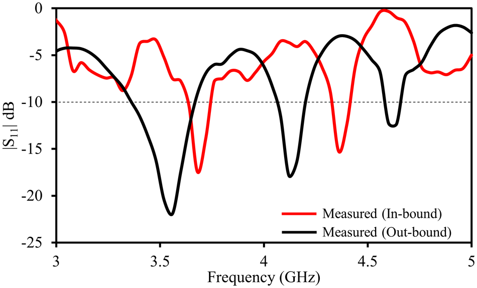
Figure 14 illustrates the comparison between measured  $|S_{11}|~dB$ values for the proposed four-element tag array in inbound and outbound configurations, respectively. A little deviation from the simulated results may be attributed to the fabrication inaccuracies and measurement errors. It is believed that using a PCB printing machine to print conductive ink traces on a polyamide substrate would minimize discrepancies between simulated and measured results. A comparative overview of the proposed four-element RFID tag array’s simulated and measured performance is given in Table 3.
Comparison of measured  $|S_{11}| ~dB$ for the proposed tag array under inbound and outbound configurations.

The RCS represents the power reflected by a target back toward the radar relative to the incident wave and can be quantified in terms of the scattered and incident electric fields. In a monostatic measurement using a VNA, the reflection coefficient  $|S_{11}|$ expresses the ratio of reflected to incident power at the port, and thus
 $|S_{11}|^2$ corresponds to the normalized backscattered power. Therefore, for a single-port device, the RCS (dB) can be expressed using Eq. (1) [Reference Skolnik32].
 \begin{equation}
RCS=10~log_{10} ~|S_{11}|^2
\end{equation}
Which numerically equals the  $|S_{11}|$ in dB.
Table 2 provides a detailed comparison between the proposed SPRT tag array and previously reported designs used specifically for antenna arrays. Direct comparison with existing work in the same category is challenging due to the limited research on chipless tag arrays, especially in wearable applications. Consequently, the comparative analysis focuses on decoupling strategies adopted in MIMO antenna systems to highlight the advantages of our approach. Prior works predominantly rely on electromagnetic bandgap (EBG) and defected ground structure (DGS) techniques in [Reference Yang and Rahmat-Samii25, Reference Gao, Cao, Fu, Quan and Chen26, Reference Yang, Liu, Xu and Gong28, Reference Tan, Wang, Wu, Liu and Kishk29, Reference Cheng, Qiu, Shen, Zeng, Li and Wang33–Reference Pei, Zhu, Wang and Wu37] for reducing mutual coupling between elements. While effective, these techniques significantly increase design complexity and fabrication cost, which is not suitable for low-cost, flexible, and space-constrained wearable scenarios. Additionally, the physical dimensions in reported works [Reference Yang and Rahmat-Samii25, Reference Gao, Cao, Fu, Quan and Chen26, Reference Meng, Ren, Wang, Xu, Zhao and Li35–Reference Pei, Zhu, Wang and Wu37] are noticeably larger, making them less practical for compact applications. In contrast, the proposed design achieves efficient coupling suppression by optimizing element orientation without requiring additional structures or increasing the overall size. Moreover, other reported works in [Reference Yang, Liu, Xu and Gong28, Reference Tan, Wang, Wu, Liu and Kishk29, Reference Cheng, Qiu, Shen, Zeng, Li and Wang33, Reference Althuwayb, Alibakhshikenari, Virdee, Rashid, Kaaniche and Atitallah34] involve intricate configurations; therefore, the proposed configuration of SPRT tag array offers a simplified, lightweight, and cost-effective solution while maintaining excellent performance, making it highly suitable for practical passive RFID applications.
Comparison between the proposed RFID tag array and existing reported works

Table 2 Long description
The table compares RFID tag array designs by decoupling method, number of elements, operating frequency, substrate and dielectric constant, physical size, maximum read range, and stated complexity. Most prior studies use two to four elements and rely on techniques such as electromagnetic bandgap structures, defected ground structures, metasurfaces, orthogonal placement, or other decoupling structures. Reported resonant frequencies span from sub 1 gigahertz bands up to 26 gigahertz, with several designs operating around 3 to 6.6 gigahertz. Substrates are commonly FR4 or RT duroid, while the proposed design uses polyimide with dielectric constant 3.5. Sizes vary widely, from about 50 by 30 mm up to 205 by 120 mm; the proposed design lists two footprints, 80 by 80 mm and 76 by 76 mm. Only the proposed design provides a maximum read range, reported as 81 to 89 mm, while all other entries leave read range blank. Complexity ratings range from low to high; the proposed design is rated low complexity, whereas many comparable four element designs are rated medium or high. Because read range is missing for the other works, direct performance ranking by range is not possible from this table alone.
Comparison of simulated and measured reflection coefficients for the proposed four-element passive RFID tag array

Table 3 Long description
The table lists reflection-coefficient minima for a four-element passive RFID tag array, giving frequency in gigahertz and return-loss magnitude in decibels for inbound and outbound cases, both simulated and measured. In simulation, inbound has dips at 3.8 GHz (minus 23.17 dB) and 4.0 GHz (minus 15.03 dB). Simulated outbound shows dips at 3.8 GHz (minus 20.72 dB), 4.04 GHz (minus 16.92 dB), and 4.68 GHz (minus 19.0 dB). In measurement, inbound dips occur at 3.68 GHz (minus 17.44 dB) and 4.36 GHz (minus 15.24 dB). Measured outbound dips occur at 3.56 GHz (minus 21.90 dB), 4.12 GHz (minus 17.80 dB), and 4.6 GHz (minus 12.29 dB). Overall, measured resonant frequencies are shifted relative to simulation, and measured dip depths are generally less negative than simulated, except the outbound dip near 3.56 GHz which is close in depth to the simulated 3.8 GHz outbound dip. The table reports only selected dip points, so it does not show full bandwidth or the complete shape of the response.
Conclusion
The paper deals with a systematic analysis of electromagnetic coupling in a two-element and four-element RFID array tags. It is observed that the orientation of each element in the proposed structure (folded outer split ring) plays a crucial role in controlling the coupling between the elements of the tag array, which in turn helps minimize EMI in both inbound and outbound scenarios. While the conventional techniques fail to control the coupling due to space constraints in wearable conditions, the proposed structure of the tag array mitigates the coupling effect by selecting the orientation of the tag element without increasing the size of the tag array. Furthermore, the SAR analysis establishes the suitability of the proposed tag array for wearable conditions. The proposed tag array design offers a comprehensive analysis of the mutual coupling and mitigation strategies essential for its reliable operation in a densely packed tag environment. Since the tag array consists of two different sizes of tags, each set of diagonal tags may be used for two different purposes, such as identification and sensing. Such tag arrays have several promising applications in the future, such as healthcare monitoring and biomedical sensing in wearable IoT systems.
Acknowledgements
This research was supported by the Department of Science and Technology (DST), Government of India, under SERB POWER Grant No. SPG/2021/002212, for which the authors are sincerely grateful.
Competing interests
The authors declare no competing interests.

Ravi Chandra received the master’s degree in Engineering from the Birla Institute of Technology, Mesra, during the period 2012–2014, where his growing interest in electromagnetic theory and antenna design led him to pursue a Ph.D. degree at the same institution. His doctoral research, completed in 2025, focused on the development of dielectric resonator MIMO antennas for modern wireless communication systems. Currently, he serves as a Junior Research Fellow at the Birla Institute of Technology, Mesra, where he is involved in the mitigation of electromagnetic interference and electromagnetic compatibility issues in wearable IoT devices.

Nisha Gupta received the bachelor’s and master’s degrees in Electronics and Communication and Electrical and Electronics Engineering, both from the Birla Institute of Technology, Mesra, Ranchi, India. She obtained her Ph.D. degree from the Indian Institute of Technology, Kharagpur, India. She was a Postdoctoral Fellow at the University of Manitoba, Canada, from 1997 to 1998, before joining the Department of Electronics and Communication Engineering, Birla Institute of Technology in 1999 as an Associate Professor. Currently, she is a Professor in the same department. She has authored and coauthored more than 150 technical journal articles and conference papers. Her research interests are Computational Electromagnetics, Antennas, AI techniques in Wireless and Mobile Communication, and EMI/EMC.

Itu Snigdh received the bachelor’s degree in Electrical Engineering from B.I.T Sindri, India, in 1996, master’s degree in Software Engineering from B.I.T Mesra (Ranchi), India, in 2002, and Ph.D. degree from B.I.T. Mesra in the area of Wireless Sensor Networks, Department of Electronics and Communication Engineering. She is an Associate Professor in the Department of Computer Science and Engineering. Her areas of interest include Cyber physical systems, IoT, Software Engineering, Database Management Systems and Wireless Sensor Networks.