Introduction
Physical vapor deposition (PVD) is a well-established and widely used technique for depositing thin films. Upon evaporation, the vaporized source material travels in a “line-of-sight” manner from the source crucible to the substrate. Because the substrate is typically oriented perpendicular to the source in conventional systems, this deposition process generally provides relatively uniform, planar layers of the deposited material. Thus, current manufacturing technologies are almost exclusively limited to top-down, two-dimensional processes unless more complex, multi-step fabrication approaches are used. However, as nanofabrication technologies advance, there is an increasing desire to create films and structures that are quasi-3D and fully 3D for various electrical and optical devices.[ Reference Jacob, Alekseyev and Narimanov 1 – Reference Kildishev and Shalaev 4 ] Angled PVD is one of the most promising approaches that can be exploited to allow fabrication of such structures. By adjusting the substrate angle, the line-of-sight deposition allows for the creation of drastically different, non-uniform, and non-conformal structures.[ Reference Suh, Huntington, Kim, Zhou, Wasielewski and Odom 5 ] In the limiting case of a large angle range, when the substrate is fixed at an angle close to 90° (commonly known as glancing angle deposition or GLAD), a conventional thin-film formation process is transformed into preferential deposition on random nucleation sites formed during the early stages of deposition.[ Reference Robbie, Sit and Brett 6 – Reference Zhao, Ye, Wang and Lu 8 ] Continued deposition atop these nucleation sites can, for example, be used to create intrinsic tilted nanowire forests due to the shadowed regions behind the nucleation sites where no material is deposited. In addition, control of the deposition angle and substrate rotation can be used to create more complex geometries such as vertical nanowires,[ Reference Zhao, Ye, Wang and Lu 8 ] chiral structures,[ Reference Mark, Gibbs, Lee and Fischer 9 ] and photonic crystals.[ Reference Jensen and Brett 10 ] Consequently, GLAD techniques could enable the bottom-up development of materials with unprecedented control over the flow of light.[ Reference Barnes, Dereux and Ebbesen 11 , Reference Lal, Link and Halas 12 ]
Angled PVD for transformation optics
One of the most exciting research directions in nanophotonics and optical metamaterials (MMs) is transformation optics (TO). Engineering the optical space by means of TO has resulted in unusual and fantastic electromagnetic devices ranging from hyperlenses with subwavelength resolution to cloaks and extreme light concentrators.[ Reference Jacob, Alekseyev and Narimanov 1 – Reference Wang, Xing, Fang, Liu, Ma, Lin, Wang and Luo 3 , Reference Liu, Lee, Xiong, Sun and Zhang 13 ] Such devices are achieved by designing the flow of light through the structure. This control is obtained by carefully designing the constituent materials and structures to define and manipulate the optical space through which light travels.[ Reference Lu and Liu 14 ] Consequently, TO requires significant freedom in the thickness, shape, structure, and conformity of the materials which is difficult to achieve through traditional methods. For example, a lens that can magnify subwavelength objects and project them into the far-field has been proposed[ Reference Jacob, Alekseyev and Narimanov 1 , Reference Kildishev and Narimanov 2 ] and demonstrated,[ Reference Liu, Lee, Xiong, Sun and Zhang 13 ] which could have a great impact on optical microscopy. However, the main challenge in fabricating such a device is the lack of technology for curved films and films of non-uniform thicknesses. Fabrication of such non-uniform, non-conformal films using angled deposition is explored in this work, which is expected to enable a family of devices with smooth gradients in both the electrical and optical properties.
Another rapidly developing research direction that will benefit from the proposed fabrication techniques is the field of plasmonics, specifically devices using alternative plasmonic materials for practical device applications.[ Reference Boltasseva and Atwater 15 – Reference Kinsey, Ferrera, Shalaev and Boltasseva 18 ] Previous research in plasmonics largely relies on using the noble metals, which can limit the performance of practical devices in many applications.[ Reference Li, Guler, Kinsey, Naik, Boltasseva, Guan, Shalaev and Kildishev 19 , Reference Guler, Ndukaife, Naik, Nnanna, Kildishev, Shalaev and Boltasseva 20 ] Alternatively, transition metal nitrides are refractory plasmonic materials, with optical properties similar to those of noble metals in both visible and near-infrared regions, that hold great advantages for practical applications due to their extreme thermal stability[ Reference Li, Guler, Kinsey, Naik, Boltasseva, Guan, Shalaev and Kildishev 19 ] and CMOS-compatibility.[ Reference Kinsey, Ferrera, Naik, Babicheva, Shalaev and Boltasseva 21 ] In addition to the standard nitride growth techniques such as sputtering, it has been recently reported that TiN nanoparticles can be obtained from TiO2 nanoparticles through a nitridation process[ Reference Guler, Shalaev and Boltasseva 22 ] which can be extended to enable the development of complex 3D transition metal nitride structures from the corresponding transition metal oxide structures. In this paper, we will show the capability of fabricating unique 3D TiO2 structures using the GLAD technique which, when combined with the nitridation processing, will potentially offer an abundance of structures for practical applications using TiN and other alternative plasmonic materials.
Results and discussion
Tapered thickness films
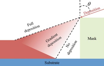
When a material is deposited at an angle, a “shadowed” region is created behind any protruding structures (Fig. 1). The side of this shadowed region further from the mask will receive the full amount of deposited material, as its line-of-sight is not impacted by the mask. Subsequently, the region of the substrate close to the mask will have no deposited material, as the line-of-sight nature of the deposition prohibits flux in this region. However, at the boundary of these two deposition zones, there will be a small region that receives a gradient of deposited flux. Due to this deposition gradient, along with surface diffusion, a thin film with a tapered thickness can be fabricated along a planar substrate. A schematic of this angled PVD technique is shown in Fig. 1, where the angle between the normal of the substrate and the deposition beam is indicated by θ.
Schematic illustration of how the angled PVD can be used to create films with gradient thickness across a planar substrate.

The samples fabricated in this work consist of alternating layers of Ag/SiO2 thin films on planar glass substrates. The choice of materials was governed by the recent device demonstrations and designs in the areas of optical MMs and TO.[ Reference Jacob, Alekseyev and Narimanov 1 – Reference Wang, Xing, Fang, Liu, Ma, Lin, Wang and Luo 3 ] The fabrication technique for the thin films deposited begins by first applying a tape mask (~60 µm thick, Kapton), which has sharp vertical sidewalls and good thermal stability, to the glass substrate before loading the sample into the chamber. Before depositing Ag on an SiO2 layer, a 1 nm germanium wetting layer was deposited at θ = 0°, which helps to promote smooth and continuous growth of Ag films on SiO2 for ultra-thin layers (below 7 nm).[ Reference Yang, Zhou, Johnson and Wadley 23 , Reference Chen, Thoreson, Kildishev and Shalaev 24 ]
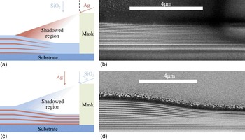
Two types of multilayered films with tapered thickness on planar substrates are demonstrated here: one with a uniform SiO2 thickness of 77 nm and Ag thickness that tapers from 20 to 0 nm, and one with a uniform Ag thickness of 10 nm and an SiO2 layer that tapers from 100 to 30 nm. The first type of tapered film was made by adjusting the substrate to an angle of θ = 80°, then depositing 20 nm of Ag. A distribution of Ag will be deposited behind the mask. Regions of the sample that are more than 80° (θ) will receive the full 20 nm of deposited Ag. Regions of the substrate below 80° will have an Ag film whose thickness tapers from 20 nm down to 0 nm. SiO2 can then be deposited at normal incidence (θ = 0°) to create a film of uniform thickness, following the contour of the underlying Ag layer. This process was then repeated 14 more times to create multilayer structures with aligned tapered thickness films that can be seen from the schematic in Fig. 2(a) and the scanning electron microscope (SEM) image in Fig. 2(b). By depositing Ag at θ = 0° and SiO2 at θ = 79.8°, tapered structures of Ag having a uniform thickness of 10 nm and SiO2 which tapers from 100 to 30 nm can be obtained [Figs. 2(c) and 2(d)]. The length of the tapered region can be adjusted by changing θ by very small amounts. For example, θ is set to be 79.8° in Figs. 2(c) and 2(d), while depositing SiO2 resulting in a tapered region shorter than that in Figs. 2(a) and 2(b), where θ = 80° while depositing Ag.
Two types of tapered thickness films on planar surfaces. (a, c) Schematics showing angled deposition for depositing Ag (a) and SiO2 (c) at an angle to produce films of tapered thicknesses. (b, d) Cross-section SEM images of the corresponding tapered multilayer films.

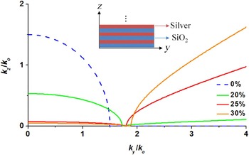
Adjusting the thickness of one material (dielectric/metal) while keeping the thickness of the other material (metal/dielectric) changes the metallic filling fraction of the films, which then leads to the modulation of the films’ in-plane permittivity. As an example, Fig. 3 shows the change of the dispersion curve as a function of filling ratio of the metal in a multilayer film composed of SiO2 and Ag. At 0%, the dispersion is spheroidal (dashed blue curve) as expected for pure silica and becomes hyperbolic with the addition of more metal. As a consequence, for the structure shown in Fig. 2(b), one can get an effective positive permittivity (dielectric) at one (thin) side of the structure, and an effective negative permittivity (metal) on the other (thick) side of the structure by choosing the appropriate deposition parameters. This strong change in effective optical properties has very interesting applications in waveguiding along this adiabatically tapered film.[ Reference West, Kinsey, Ferrera, Kildishev, Shalaev and Boltasseva 25 ] One recent study also demonstrates the usefulness of these structures for enabling new types of light-emitting sources with high efficiency.[ Reference West, Kinsey, Ferrera, Kildishev, Shalaev and Boltasseva 25 ]
Iso-frequency curves in k-space (dispersion) at 476 nm for the multilayer Ag/SiO2 structure and various metal filling fractions from 0 to 30%.

Curved nanostructures
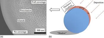
Due to the line-of-sight nature of PVD, in the case of non-planar surfaces, the amount of material deposited will change with the curvature. In the case of a spherical particle, for example, the surface which is normal to the deposition direction will receive the entire deposition flux, while the edges of the particle will receive only a glancing (close to zero) amount of material. Consequently, the curved surface will result in a distribution in the film thickness across the sphere [Fig. 4(b)]. By adjusting the deposition angle and rotating the sample, this evaporation technique allows for great control over this thickness gradient from any angle along the curved surface.
A 5 µm-diametered SiO2 microsphere with 40 nm Ag deposited at a 45° angle. (a) Distribution in thickness ranging from no coverage to full continuous coverage. (b) A schematic showing the deposition angle of the incident Ag flux, the shadowed region behind the microsphere and the thickness gradient along the sphere.

To demonstrate this film thickness gradient, 40 nm of Ag was deposited directly on a 5 μm-diametered SiO2 microsphere at an angle of 45° [Figs. 4(a) and 4(b)]. The growth dynamics of Ag films on SiO2 have been studied in depth and thin-film formations have been previously analyzed.[ Reference Yang, Zhou, Johnson and Wadley 23 , Reference Chen, Thoreson, Kildishev and Shalaev 24 ] When the effective deposited thickness is below 10 nm, Ag will form isolated “islands”. When the effective thickness is about 10 nm, the deposited Ag becomes a percolated film, and when the effective thickness approaches 20 nm, the film becomes continuous. Figure 4(a) demonstrates a clear effective thickness gradient of the deposited Ag across a microsphere. Because the total deposited thickness at normal incidence on the sphere is 40 nm, the entire range of the film structure (continuous, percolated, islands, and eventually uncoated SiO2), can be seen.
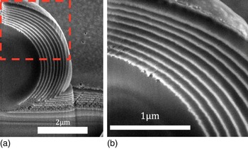
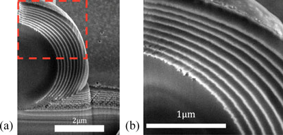
There has been recent interest in the optics community to make devices such as planar hyperlenses and optical concentrators[ Reference Jacob, Alekseyev and Narimanov 1 , Reference Kildishev and Narimanov 2 ] requiring non-uniform layer thicknesses on curved surfaces. Since a nanocavity can be scaled down to subwavelength dimensions, plasmonic nanolasers, and spasers[ Reference Noginov, Zhu, Belgrave, Bakker, Shalaev, Narimanov, Stout, Herz, Suteewong and Wiesner 26 ] can also be fabricated using a similar core–shell structure of alternating metal/dielectric layers. Many of these devices make use of alternating thin films of metal and dielectric layers, which are thicker on the horizontal sides of a cylindrical (or spherical) core, and thinner on the top of the structure. These curved layers of varying thickness can be fabricated by combining the curved surface with angled deposition. By following this procedure at an angle of 86°, larger amounts of material will accumulate on the outer edges of the sphere, while very little of the material is deposited on the top of the structure—providing the desired structure as shown in Fig. 5(a).
SEM images of a 5 µm-diametered silica microsphere coated by multilayered film with gradient thicknesses, where (a) shows one half of the microsphere, while (b) is an inset, emphasizing the difference in film thicknesses between the top and sides of the sphere.

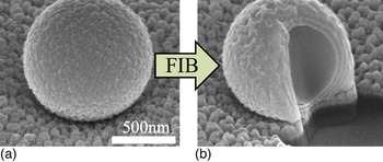
Depositing materials at glancing angles on a structure (such as the top of the sphere in Fig. 5), will typically result in the growth of nanowires—due to the strong shadowing effect at large angles as discussed in the previous section. To reduce or eliminate this wire growth, a thin layer of germanium is applied around the entire sphere beneath each Ag layer. This layer helps reduce surface roughness and eliminate nanowire growth on regions of the structure that receive glancing deposition. Additionally, rotating the sample and depositing small amounts of material over the small islands will also help reduce the region's roughness. Using a similar technique, multiple uniform layers of materials can be deposited to create “core–shell” structures. Continuously rotating and tilting the substrate during deposition creates continuous films around the sphere despite the layer thicknesses remaining relatively thin (about 13 nm). An example of such a core–shell structure can be seen in Fig. 6.
A 1 µm-diametered SiO2 microsphere before (a) and after (b) a focused ion beam cut. Although layers are only about 13 nm each, they remain relatively smooth and uniform.

Several additional notable effects must be taken into consideration when growing thin films on curved surfaces, beyond the purely “line-of-sight” nature of the deposition. First, surface diffusion will have an impact on the final structure.[ Reference Wang and Zhao 27 ] The effects of surface diffusion are non-trivial and depend on several variables—including the surface energy of the deposited material and its underlying layer, substrate temperature, and deposition rate. Although employing germanium as a wetting layer will improve the growth of Ag on SiO2, substrate temperature monitoring and cooling will also help this issue. Second, it should also be noted from Fig. 5(a) that despite the material being deposited at a sharp glancing angle (normal to the sides of the spheres), the deposited material will accumulate on the substrate and beneath the sphere. This would require special measures to eliminate and should be taken into account when using this type of deposition process. Third, although material can be deposited all around the outside of the sphere, there will always be an opening at the bottom of the sphere where no material can be deposited (i.e., the bottom of the object in contact with the substrate). Fourth, although only the deposition onto spherical particles has been discussed, these methods are valid for other curved surfaces.
TiO2 nanostructures
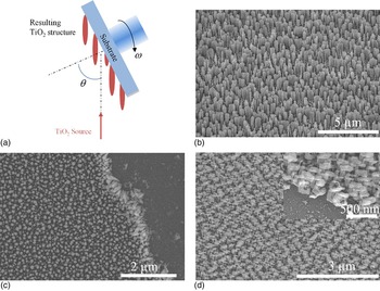
The GLAD technique also offers opportunities to fabricate 3D dielectric structures, such as metal oxides, on a large scale suitable for many potential applications.[ Reference Robbie, Sit and Brett 6 , Reference Hawkeye and Brett 7 , Reference Jensen and Brett 10 , Reference Zhao 28 , Reference Kiema, Colgan and Brett 29 ] For example, it has been demonstrated that nanoporous TiO2 films prepared by GLAD are beneficial for solar cell applications providing high surface area, tight interfaces, and enhanced light trapping.[ Reference Wong, Lee, Chen and Huang 30 ] One example of these dielectric nanostructures is a tilted TiO2 nanorod array, which can be fabricated by depositing at a steep angle (θ = 86°) with respect to the substrate normal with no azimuthal rotation (ω = 0) as shown in Fig. 7(a). The resulting TiO2 nanorods are uniform on a large scale with a tilt angle of 34° with respect to the substrate surface [Fig. 7(b)]. The dimensions and alignment of the nanorods, such as the nanorod length, tilt angle, and density, can be tuned by properly changing the evaporation angle (θ), deposition rate, and azimuthal rotation (ω). For example, if continuous rotation is applied to the substrate during deposition (ω = 0.05 rad/s, θ = 86°), vertical TiO2 nanorod arrays can be obtained [Fig. 7(c)]. This technique can also enable a chiral zigzag structure [Fig. 7(d)]. This structure is obtained by rotating the substrate 90° counterclockwise after depositing 120 nm TiO2 each time while keeping θ = 86°, leading to the chiral zigzag structure in Fig. 7(d) (shown with six deposition iterations). More complex structures could be obtained by programing the tilt angle θ and the azimuthal rotation ω of the substrate properly. Furthermore, as mentioned above, these TiO2 structures can be transformed to TiN which is an appealing plasmonic material due to its extraordinary thermal stability, and CMOS-compatibility, and thus we can envision the important role of GLAD in the area of nanophotonics.
Fabrication of various TiO2 nanostructures using GLAD. (a) Schematic of fabricating TiO2 nanostructures. (b–d) Top-view SEM images of the tilted nanorod array (b), vertical nanorod array (c), and chiral zigzag array (d).

Conclusions
In this work, we report several techniques based on angled PVD that take advantage of the line-of-sight nature of PVD and enable additional degrees of freedom for non-planar fabrication. Tapered multilayer films with non-uniform gradient thicknesses were deposited on planar substrates with the help of masks, which could find their applications in TO and enhancing the performance of light emitters. Quasi-3D thin films were demonstrated on the spherical surfaces whose thickness gradient can be designed through control of the deposition angle, substrate rotation, etc. These structures perfectly meet the needs of realizing several TO devices such as superlenses and advanced cavities for nanolasers. We have also extended our approach beyond noble metals and presented the fabrication process of 3D nanostructures made of TiO2. Using recently developed nitridation procedures, these transition metal oxide nanostructures could be made plasmonic which will bring practical applications of numerous plasmonic structures within reach. Here, access to a wide variety of geometries that can be realized in transition metal nitrides holds a great promise for applications that require high thermal stability and CMOS-compatibility. Subsequently, angled PVD has been shown as a powerful yet flexible method in fabricating advanced nanophotonic and electronic structures.
Acknowledgment
We would like to acknowledge ARO MURI grant 56154-PH-MUR (W911NF-09-1-0539).