Introduction
Future electronics, without a doubt, are going to take a different form: We are going to put them on curved surfaces; we are going to bend and fold them. Enabling such future electronics will require new materials that not only have exceptional electronic properties, but also possess high mechanical tolerance. For example, if we are going to wear electronics, then the strain tolerance will need to be in the range of 50–80%, depending on the location where we wear them. Bendable displays require a strain tolerance greater than 50% if the radius of curvature is less than 1 mm.
So where do we get inspiration to design future generations of electronic materials? In our case, we use human skin as an inspiration. Human skin is a material that combines properties such as flexibility, stretchability, biodegradability, and self-healing properties with sensing functionalities. If we are able to mimic all of these functionalities of human skin and incorporate them into our future electronic materials, this will potentially open up many new exciting possibilities.
A number of prospective applications will be made possible with skin-inspired devices, for example, in robotics, medical devices, automobiles, and consumer electronics. There are different approaches to realize skin-inspired electronics. One approach, pioneered by the Rogers group, is to take rigid inorganic materials and make them ultrathin, and through structural design, make them stretchable and bendable so they are able to be placed onto curved surfaces. Reference Rogers, Someya and Huang1–Reference Kim, Ahn, Choi, Kim, Kim, Song, Huang, Zhuangjian, Chun and Rogers4 In my group, we take a different approach. We begin by redesigning electronic materials, and we aim to build a path to incorporate different functionalities stepwise into these new generations of electronic materials. Therefore, we work with organic materials, polymers, and carbon nanomaterials because through molecular engineering, we can potentially modify their properties—not only the electronic properties, but also mechanical properties. Furthermore, these materials can be processed over a large area, potentially even using a roll-to-roll coating method, such that the related electronic devices can take advantage of additive and scalable manufacturing.
Our vision is to understand the materials design required for the basic components, such as solar cells, sensors, integrated circuits, and batteries; all of these will mimic the properties of human skin. In the near future, we would like to use these devices to enable applications in health monitoring, environmental monitoring, and, in the intermediate term, for displays, robotic applications, and automobiles. Over a longer term, we hope to use such electronics to interface with the human body to enable implantable medical devices.
Current electronics are already flexible, to an extent. However, in the future, we would like to add new functions: stretchability, biodegradability, and self-healing properties. The important questions we try to address are threefold. The first is from the fundamental side: How do we make organic and carbon electronic materials better since their electronic properties are still not as good as some inorganic materials? The next question with such materials is how do we add additional functionalities? And finally, with the new materials we develop, what are the applications that are enabled because of their unique properties?
Skin inspiration
Overall, the bigger picture that we use to drive our thinking about how we design materials and how we structure our research strategy is based on this question: how do we build a piece of artificial electronic sheet that has a similar “feel” and function to human skin but is additionally able to communicate with our brain? If we are able to understand how to design all of the materials that will enable this vision, then many new applications will also be enabled along the way. In order to realize this vision, we need to first understand how our skin communicates with the brain, and then divide this problem into device and materials requirements that we need in order to build this artificial electronic sheet.
First, we consider how our skin functions in terms of sensing external stimulations. There are various kinds of receptors in skin. Reference Vedel and Roll5 Mechanoreceptors are responsible for the sensing of pressure. They are able to communicate with the brain because an applied pressure triggers mechanoreceptors to generate electrical pulses, which are subsequently transmitted through nerve bundles to the brain. A slow-adapting mechanoreceptor is a type of mechanoreceptor that allows us to sense the amplitude of pressure. The basic behavior of the observed electrical signals fired by slow-adapting mechanoreceptors have been experimentally measured previously and reported. Reference Vedel and Roll5 The general observed trend is that as the force or pressure increases, the frequency of such pulses will increase—a digital format of an electrical signal is transmitted through our nervous system. The human body uses this approach in processing data because this approach consumes less power and tolerates more errors, thus, electrical signals can transmit over a long distance.
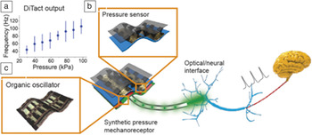
We want to mimic this process and use developed organic materials and carbon nanomaterials to build a platform that will potentially allow us to add additional functionalities into the platform with increasing complexity over time. We have developed a Digital Tactile System (DiTacts) ( Figure 1 ) that includes sensors to sense an external stimulus; circuits are then used to process the signal and generate the electrical pulses needed to communicate with the brain. Reference Tee, Chortos, Berndt, Nguyen, Tom, McGuire, Lin, Tien, Bae, Wang, Mei, Chou, Cui, Deisseroth, Ng and Bao6
Our Digital Tactile (DiTact) System to mimic biological mechanoreceptors, which generate digital signals, as shown in (a). It combines (b) a sensor with (c) a printed organic transistor circuit that generates electrical pulses used to stimulate the brain. Such a system consumes less power and tolerates more errors. Reprinted with permission from Reference Reference Tee, Chortos, Berndt, Nguyen, Tom, McGuire, Lin, Tien, Bae, Wang, Mei, Chou, Cui, Deisseroth, Ng and Bao6. © 2015 AAAS.

Sensing element for DiTacts
There are a number of different strategies that can be implemented to realize a pressure sensor. The applied force will result in a corresponding change in the electrical signal. When we started this work in 2006, Someya’s group at The University of Tokyo reported one of the early examples that showed the promise of organic materials for application in artificial skin, where various pressure sensors and temperature sensors were integrated onto stretchable substrates. Reference Someya, Sekitani, Iba, Kato, Kawaguchi and Sakurai7 The flexible sensor that was available then was a conductive rubber pressure sensor using a rubber matrix mixed with carbon black. This can provide a flexible pressure sensor; however, it is not very sensitive, and tends to be quite thick. It was a challenge to make it thin, conformal, and sensitive.
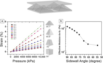
We first developed a skin-mimicking pressure sensor to help mimic the touch function of human skin. Reference Mannsfeld, Tee, Stoltenberg, Chen, Barmann, Muir, Sokolov, Reese and Bao8 We initially started out simple: we thought we could take a capacitor and sandwich a layer of elastomer, such as cross-linked poly(dimethylsiloxane), between two pieces of conductor to make a pressure sensor. It turned out that when we made the layers paper-thin, the device was not sensitive and not reproducible. Additionally, a high applied force greater than a few kPa was needed to deform the thin layer of rubber. This led to a new idea to fabricate ultrathin devices that are highly responsive to pressure, similar to human skin. We did this by designing many small air gaps into the thin rubber structure, such as using periodic structures of pyramids or lines, which will allow the rubber to be easily compressed by small, applied pressure, as small as a few Pa ( Figure 2 ). The device then becomes highly sensitive to pressure. Reference Mannsfeld, Tee, Stoltenberg, Chen, Barmann, Muir, Sokolov, Reese and Bao8,Reference Tee, Chortos, Dunn, Schwartz, Eason and Bao9
The microstructured rubber with pyramid structures significantly increases sensitivity of the pressure sensor. Simulation data showing (a) predicted stress–strain (σ–ε) relationships of different side wall angled microstructures where higher sensitivity for structures with higher slopes is observed; and (b) predicted effective modulus of the microstructures showing almost one order of magnitude decrease as the side wall angle decreases. Reprinted with permission from Reference Reference Tee, Chortos, Dunn, Schwartz, Eason and Bao9. © 2014 Wiley.

Modeling data show that different shapes of rubber (i.e., with different slopes of the pyramid side walls) can result in a different degree of response to the same applied pressure (Figure 2). Reference Tee, Chortos, Dunn, Schwartz, Eason and Bao9 The greater the slope, the less displacement of the rubber at the same applied pressure, and therefore less sensitivity. Reference Tee, Chortos, Dunn, Schwartz, Eason and Bao9 By tuning the shape and dimensions of the pyramidal structures, we can effectively tune the sensitivity of the sensors.
We compared the sensitivity of a thin film versus line and pyramid structures. Even though a thin film can respond to pressure, its sensitivity compared to the pyramid and line structures is much lower. The high sensitivity allows us to detect very low pressures (e.g., 20 mg weight over an area of 1 cm2). This observed pressure value is a few hundred times lower compared to the value asserted by gentle touch. If you use your finger to gently touch your skin, the pressure applied is already on the order of a few kilopascal, so these very thin (less than 100 μm in thickness) and flexible sensors have much higher sensitivity compared to our skin.
These rubber structures can be combined with different sensor designs. For example, to make a resistive pressure sensor, the pyramid structure is coated with carbon nanotubes such that the contact area with the adjacent electrode changes the amount of current that conducts through the material. Reference Tee, Chortos, Berndt, Nguyen, Tom, McGuire, Lin, Tien, Bae, Wang, Mei, Chou, Cui, Deisseroth, Ng and Bao6 Again, a pyramid structure makes the device highly responsive to pressure.
One challenge with resistive sensors is that a constant current always flows through the device. This results in undesirably high power consumption. We designed a new type of resistive sensor where we removed the conductive material from the tips of the pyramids such that no conduction occurs when no pressure is applied. On the other hand, when we apply a pressure, the conductive regions come in contact with the top electrode, and current starts to flow through. Reference Chou, Nguyen, Chortos, To, Lu, Mei, Kurosawa, Bae, Tok and Bao10 Such a design can, therefore, significantly reduce power consumption.
One possible way to read the value and location of an applied pressure, instead of directly reading electrical conduction values, is to use a color-indication map similar to the skin color change of a chameleon. Specifically, chameleon skin changes color depending on its surroundings. To mimic this skin function, we integrated our resistive sensors with electrochromic devices in which the color of the electrochromic polymer is controlled by the applied voltage, which, in turn, is controlled by applied pressure. Reference Chou, Nguyen, Chortos, To, Lu, Mei, Kurosawa, Bae, Tok and Bao10
Polymers as the active electronic material allow for incorporating skin-inspired functions. If we want to make a sensor that is biodegradable, we can replace the rubber dielectric material and the substrate with biodegradable elastomeric materials. Reference Boutry, Nguyen, Lawal, Chortos, Rondeau-Gagné and Bao11 The conductors can be replaced with biodegradable metal such as magnesium and iron, which are approved by the US Food and Drug Administration. With these materials, the entire device can be made biodegradable while still having a high sensitivity capable of detecting a grain of salt. The degradation kinetics of such devices can be controlled by tuning the polymer chemical structures.
Stretchability is another feature that we want to incorporate into our sensors. To make the sensors stretchable, we first replaced the metal electrodes with stretchable carbon nanotube electrodes that we previously developed. Reference Lipomi, Vosgueritchian, Tee, Hellstrom, Lee, Fox and Bao12 Then we used a slightly different design for the rubber structure such that it can remain sensitive to pressure while being able to bounce back and forth without sticking to the substrate after pressure is released. Reference Park, Kim, Vosgueritchian, Cheon, Kim, Koo, Kim, Lee, Schwartz, Chang and Bao13 The carbon nanotube electrode we developed is particularly suitable as a stretchable electrode. It is prepared by coating a layer of carbon nanotubes on a stretchable substrate. It is subsequently subjected to a strain. By tuning the interface energy of the substrate and its interaction with the nanotubes, releasing the strain results in nanobuckles or nanosprings in the nanotube film. After this initial “programming stage,” the nanotube film can be stretched up to the same initial strain level without changing the conductivity. If we want the material to tolerate a strain of up to 100%, we would prestrain the film to this level and release it. Afterward, we can re-stretch this film up to 100% strain more than 10,000 times without changing the conductivity. This is an effective way to introduce stretchability in electronic devices. Reference Lipomi, Vosgueritchian, Tee, Hellstrom, Lee, Fox and Bao12
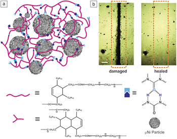
We also want to incorporate the capability for self-healing into our electronic devices. For this application, we designed a polymer composite in which the polyurethane polymer incorporates dynamic bonds for cross-linking. Reference Tee, Wang, Allen and Bao14 The dynamic bonds are hydrogen bonds that can break readily under stress when the material is subjected to strain, but they can also recover rapidly, even at room temperature. If we were to design the polymer network such that the polymer backbone has the ability to move around at room temperature or at a desired temperature, then the dynamic reactive groups such as the hydrogen bonds will be able to find each other and reform the chemical bonds. As shown in Figure 3 , two pieces of cut material are placed back together for the recovery of this crack. The cut can be readily healed at room temperature or at a slightly elevated temperature of about 50°C. Reference Tee, Wang, Allen and Bao14 The material becomes conductive by incorporating conducting nickel particles with nanospikes. We have shown pressure sensing using these types of self-healing electronic materials.
Self-healing electronic material. (a) Chemical structure of the self-healing polymer composite material with micro-sized Ni particles. (b) Optical photographs of damaged and healed films. The dashed boxes indicate the damaged and healed regions, respectively. Scale bar = 1 mm. Reprinted with permission from Reference Reference Tee, Wang, Allen and Bao14. © 2012 Nature Publishing Group.

Interfacing sensors with the brain
The next step is building the circuit needed to generate electrical pulses such as the skin mechanoreceptor. There are different approaches for interfacing sensors with the brain. A sensor usually generates an analog signal, which means it gives various pressure values over time. However, analog signals cannot be directly used to interface with the brain. They need to be converted into digital signals— electrical pulses that can be transmitted through the nervous system. The typical method to accomplish this is to take all the sensor outputs and wire them into a central microprocessor to collect and process the data. However, there are 17,000 sensors in one human hand. To process such a vast amount of data requires significant computing power and is energy intensive. Additionally, signal amplification is needed if the data are to be transmitted over a long distance from different regions of the body. The D.-H. Kim group at Seoul National University made a demonstration in which the flexible e-skin sensor signals were processed with a microprocessor and were subsequently used for nerve stimulation. Reference Kim, Lee, Shim, Ghaffari, Cho, Son, Jung, Soh, Choi, Jung, Chu, Jeon, Lee, Kim, Choi, Hyeo and Kim15
Conversely, for biological systems, the sensed signal is processed at the front end (i.e., the signal from the sensor is directly output as a digital signal) as spikes at different frequencies, depending on pressure. This transduction mechanism is inherently power efficient and robust to noise, allowing for mechanical sensations to be transmitted over long distances, such as from the extremities. A biomimetic mechanoreceptor with frequency-encoded output is the next important step toward enabling neural prosthetic devices with seamless tactile sensational feedback.
In order to generate frequency-encoded output, we combined our sensor with a simple three-stage ring oscillator circuit. Reference Tee, Chortos, Berndt, Nguyen, Tom, McGuire, Lin, Tien, Bae, Wang, Mei, Chou, Cui, Deisseroth, Ng and Bao6 A three-stage complementary metal oxide semiconductor ring oscillator consists of six transistors. Its oscillation frequency depends on the applied voltage. A low-oscillation frequency is observed with a low-applied voltage.
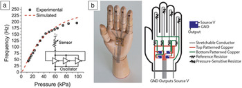
Next, we build our artificial mechanoreceptor according to a simple scheme (as shown in Figure 4b). Reference Tee, Chortos, Berndt, Nguyen, Tom, McGuire, Lin, Tien, Bae, Wang, Mei, Chou, Cui, Deisseroth, Ng and Bao6 A pressure sensor is used to control the voltage drop across the ring oscillator. When there is applied pressure, the current flow through the pressure sensor increases such that a lower voltage is distributed over the pressure sensor, and more voltage is applied to the ring oscillator. As a result, the frequency of the ring oscillator increases. The artificial mechanoreceptor outputs a similar frequency range and trends as a biological mechanoreceptor, as shown in the plot in Figure 4a.
Digital Tactile (DiTact) output and circuit details. (a) Schematic layout of DiTact sensor (inset) and plot of frequency output as a function of pressure for an example DiTact sensor, showing increased frequency with sensed pressure, similar to biological slow-adapting mechanoreceptors. (b) Image and circuit schematic of a model hand with DiTact sensors on the fingertips connected with stretchable interconnects. Reprinted with permission from Reference Reference Tee, Chortos, Berndt, Nguyen, Tom, McGuire, Lin, Tien, Bae, Wang, Mei, Chou, Cui, Deisseroth, Ng and Bao6. © 2015 AAAS. Note: V, voltage; V ss, voltage applied between source electrodes; GND, ground.

We can leverage the tremendous developments that have occurred over many years in the field of organic electronics. Starting from the mid-1980s, the first organic transistor was reported, even though it possessed several orders of magnitude lower charge-carrier mobility than amorphous-Si transistors. Reference Tsumura, Koezuka and Ando16 Currently, the mobility of a number of organic semiconductors has already exceeded 10 cm2/Vs, which is of similar order to that of polysilicon. Reference Kang, Yun, Chung, Kwon and Kim17–Reference Sundar, Zaumseil, Podzorov, Menard, Willett, Someya, Gershenson and Rogers20 This opens up many new possibilities for building circuits more complicated than the ring oscillator for more complex biomimetic artificial skins described earlier.
We used an inkjet-printing method to print the ring oscillators, completed in collaboration with T. Ng and P. Mei at Xerox PARC. They developed a process to reproducibly print organic transistor circuits. Compared to the biological mechanoreceptors, the output of the artificial mechanoreceptor shows a similar trend, where an increased force results in increased electrical pulse frequency. Reference Tee, Chortos, Berndt, Nguyen, Tom, McGuire, Lin, Tien, Bae, Wang, Mei, Chou, Cui, Deisseroth, Ng and Bao6
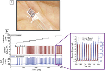
Figure 5 shows a photograph of the DiTact sensor with artificial mechanoreceptors. The next task is to connect it to the brain to see whether the output signal can be used to stimulate the brain. This can be achieved in several ways. Electrical stimulation is a well-known method where electrodes are used to directly contact and stimulate the nervous system. The advantage is that it is simple, but the disadvantage is that it is invasive, since the electrodes are typically made with hard metal, and the stimulation tends to be non-specific. All regions in contact with the electrodes are stimulated, and one cannot selectively stimulate only those nerve bundles that are responsible for detecting touch. Recently, a new technique called “optogenetics” has been developed. Reference Deisseroth21 Specific neurons are selectively genetically modified such that they can be stimulated by light pulses. This stimulation method is specific and noninvasive, even though optogenetic stimulation in humans has not yet been demonstrated.
Digital Tactile (DiTact) sensor is used for brain stimulation. (a) Photographic image of a DiTact sensor, consisting of a millimeter-sized pressure sensor and a printed organic ring oscillator. (b) Correlation among pressure, sensor output, and cell potential. As the applied pressure increases, the output voltage frequency of DiTact increases, similar to the behavior of biological mechanoreceptors. The expanded section shows that the neuron action potentials closely follow the pulses from the light-emitting diode used to stimulate the brain. Reprinted with permission from Reference Reference Tee, Chortos, Berndt, Nguyen, Tom, McGuire, Lin, Tien, Bae, Wang, Mei, Chou, Cui, Deisseroth, Ng and Bao6. © 2015 AAAS.

Because it is readily accessible, we took advantage of optogenetics to demonstrate stimulation of the brain using artificial mechanoreceptors. In collaboration with the Deisseroth group, we used our sensor output to control a light-emitting diode, which sends light pulses controlled by the frequency of the ring oscillator. Reference Tee, Chortos, Berndt, Nguyen, Tom, McGuire, Lin, Tien, Bae, Wang, Mei, Chou, Cui, Deisseroth, Ng and Bao6 We then measured the action potential generated by a slice of brain that was genetically modified to become sensitive to light stimulation. Figure 5b shows the applied pressure increasing with time. The spikes in the second plot (sensor output) are output signals from the artificial mechanoreceptor, which increase in frequency over time due to the increase of sensed pressure. Finally, the measured action potential pulses (cell potential) from the slice of brain exactly follow the frequency of the light stimulation, indicating that the brain is responding to the stimulation. This observation demonstrates that the artificial mechanoreceptor mimics the function of a biological mechanoreceptor.
With the demonstration of an artificial skin that possesses mechanoreceptor functions, we have established a path toward new generations of artificial skin with more complexity and functionalities. Our first generation only possesses flexibility, but in the future, we hope to add additional functionalities into this artificial skin sheet, such as stretchability, biodegradability, and self-healing.
Beyond artificial skin
Artificial skin may serve as an inspiration, such that the materials and devices developed for artificial skin will also enable other more near-term applications. For example, highly sensitive pressure sensors have been tested in pressure-sensitive trackpad applications. Reference Tee, Chortos, Dunn, Schwartz, Eason and Bao9 We demonstrated an example of a 130-pixel pressure-sensitive trackpad prepared in collaboration with Synaptics Co. The pressure input provides an additional way for interfacing with the computer. Reference Tee, Chortos, Dunn, Schwartz, Eason and Bao9
Another application enabled by the ultrasensitive pressure sensor is wearable electronics. Reference Schwartz, Tee, Mei, Appleton, Kim, Wang and Bao22 These thin, conformal sensors allow sensitive detection of detailed pulse wave forms that can be used to extract useful medical information about artery stiffness and blood pressure.
A wireless pressure sensor can also be readily fabricated for potential use for implantable devices. Reference Chen, Tee, Chortos, Schwartz, Tse, Lipomi, Wong, McConnell and Bao23 In this case, a thin and small wireless pressure sensor is constructed by combining the structured rubber with coil electrodes such that the applied pressure will change the resonant frequency of the coil. This sensor was implanted between the skull and the brain of a mouse, potentially allowing for monitoring brain pressure.
Self-healing is a function we would like to incorporate into electronic materials. We have developed a self-healing conductor that can undergo repeated autonomous healing at room temperature. Reference Tee, Wang, Allen and Bao14 We have also developed various self-healing polymers, some of which have very fast healing speeds. For example, one of the materials has graphene oxide as the covalent cross-linker. Reference Wang, Liu, Allen, Tok, Wu, Zhang, Chen and Bao24 After cutting it into two pieces, within one minute, this material can heal and be stretchable again. The fracture strain for this material can recover to more than 75% of its original value after one minute. With self-healing electronic materials, we demonstrated the first self-healing electronic skin that can sense pressure and strain.
The pursuit of skin-inspired electronics has motivated us to develop a new generation of electronic materials, such as self-healing conducting materials. With this material in hand, we explored other possible applications. We discovered that this material is particularly effective as a binder to enable more robust Si anodes for lithium-ion batteries. Reference Wang, Wu, Chen, McDowell, Cui and Bao25 Conventional lithium-ion battery anodes are made with graphite. Even though the theoretical charge capacity for Si is 10 times higher, poor cycling stability has been observed due to the large volume change during charging and discharging. Silicon nanostructuring has been shown to be an effective method to address this issue, but this approach is too expensive for practical implementation. Using our self-healing conducting material as a binder material, we are able to achieve high-cycling stability and high-areal capacity for the first time using low-cost, abundant silicon powder as the active material without modification of the silicon powder. Reference Wang, Wu, Chen, McDowell, Cui and Bao25
Summary
This article has outlined our recent progress toward realizing our ultimate goal of developing an artificial skin for prosthetics applications. We have developed various sensors and circuits, all of which are based on organic materials, polymers, and carbon nanomaterials. These materials provide a long-term path toward adding various skin-inspired functions. Along the way to this goal, we have delivered several exciting and useful applications, ranging from 3D electronics, Reference Wang, Wang, Tee, Kim, Lopez, Cai and Bao26 durable electronics, Reference Chortos, Koleilat, Pfattner, Kong, Lin, Nur, Lei, Wang, Liu, Lai, Kim, Chung, Lee and Bao27 health-monitoring wearable electronics, Reference Schwartz, Tee, Mei, Appleton, Kim, Wang and Bao22,Reference Chen, Tee, Chortos, Schwartz, Tse, Lipomi, Wong, McConnell and Bao23 and energy-storage devices, Reference Wang, Wu, Chen, McDowell, Cui and Bao25 due to the availability of new electronic materials.
Acknowledgments
This work received support from the National Science Foundation, Air Force Office of Scientific Research, Global Climate and Energy Program, Samsung Electronics, and BASF.

Zhenan Bao is a professor of chemical engineering at Stanford University. Prior to joining Stanford in 2004, she was a distinguished member of the Technical Staff in Bell Labs, Lucent Technologies from 1995 to 2004. She has more than 400 refereed publications and more than 60 US patents. Her current research focuses on skin-inspired organic electronic materials. Bao is a member of the National Academy of Engineering. She is a Fellow of MRS, ACS, AAAS, SPIE, ACS PMSE, and ACS POLY. She is an associate editor for Chemical Science. Her recent awards include the L’Oreal Women in Science Award 2017, ACS Applied Polymer Science Award 2017, Nature’s Ten People Who Mattered in 2015, AIChE Andreas Acrivos Award for Professional Progress in Chemical Engineering in 2014, ACS Carl Marvel Creative Polymer Chemistry Award in 2013, and ACS Cope Scholar Award in 2011. Bao’s research group website is baogroup.stanford.edu and she can be reached by phone at 650-723-2419 or by email at zbao@stanford.edu.