I. INTRODUCTION
III-Nitride semiconductors and their alloys are of increasing scientific and technological interest in the applications of novel optoelectronic devices due to their wide band gap and excellent electronic and optical properties.Reference Ponce and Bour 1 – Reference Khan, Shatalov, Maruska, Wang and Kuokstis 7 In general, functional heterostructures, e.g., multiple quantum wells and superlattices, have been widely used in device fabrication owing to their distinct virtues such as lower threshold current density, lower nonradiative recombination rate, sharper emission spectra, and reduced sensitivity to temperature.Reference Sitar, Paisley, Yan, Ruan, Choyke and Davis 8 Particularly, GaN/AlGaN heterostructures have attracted tremendous attention over the past decades as a significant potential for GaN-based electronic and optical applicationsReference Hoshino, Someya, Hirakawa and Arakawa 9 – Reference Asgari, Ahmadi and Kalafi 12 due to their excellent properties, e.g., high conduction band offset, large longitudinal phonon energy, and ultrafast carrier and intersubband relaxation. In addition, an increasing research effort has been directed toward the investigation of intersubband transitions in GaN/AlGaN quantum size structures, which possess broad applications in, e.g., infrared photodetectors, quantum cascade detectors, and electrooptic modulators.Reference Baumann, Giorgetta, Hofstetter, Lu, Chen, Schaff, Eastman, Golka, Schrenk and Strasser 13 – Reference Nevou, Kheirodin, Tchernycheva, Meignien, Crozat, Lupu, Warde, Julien, Pozzovivo, Golka, Strasser, Guillot and Monroy 16 As the main active component, the achievement of high quality GaN/AlGaN heterostructures becomes extremely critical in fabricating optoelectronic devices with high performance.
However, due to the large lattice and thermal mismatch between the sapphire substrate and the epilayer, the difficulty in achieving high crystalline quality of high Al-content AlGaN restricts the improvement of GaN/AlGaN heterostructures. Moreover, the most critical part of a heterostructure is the interface between heterolayers, which plays the key role in deciding its function and property. To achieve abrupt interface, an interruption treatment with ammonia flow between the growth of the well and barrier has been introduced to the InGaN/GaN heterostructures, and the structural and optical properties have been reported significantly improved.Reference Moon, Kim, Song, Kim, Yi, Noh and Park 17 Although the growth interruption technique has also been used in GaN/AlGaN heterostructures,Reference Shirasawa, Mochida, Inoue, Honda, Sakaguchi, Koyama and Iga 18 due to the complicated condition of surface growth and the small scale of the interfacial layers, the effect on the abruptness of interfaces has not been systematically studied and the refined scheme for interfacial improvement is lack.
In this work, the interface abruptness of the GaN/AlGaN superlattices structure with various growth interruption conditions was studied and an asymmetry of different types of interfaces in the superlattices was observed. The group III sources were shut off at different interfaces between the GaN well and AlGaN barrier layers, and various duration of NH3flow at this growth interruption period were carried out. With x-ray diffraction (XRD) and high-resolution transmission electron microscopy (HRTEM), it was found that the interface abruptness is highly associated with the time of growth interruption, and the sharpness of the GaN/AlGaN interface and the AlGaN/GaN interface appear distinct asymmetric. Based on the understanding of the possible reasons causing the interface asymmetry, an alternative growth interruption scheme was proposed to improve the interface quality, and consequently, the emission efficiency of the superlattices could be significantly enhanced.
II. EXPERIMENTAL DETAILS
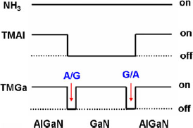
The GaN/AlGaN superlattices structures were grown by metalorganic chemical vapor deposition with a Thomas Swan closely coupled showerhead reactor (Herzogenrath, Germany), which is designed especially for reducing the undesired gas phase parasitic reaction. The trimethylgallium, trimethylaluminium (TMAl), and ammonia (NH3) were used as the precursors for Ga, Al, and N, respectively, and H2 and N2 were used as the carrier gases. Prior to the GaN/AlGaN superlattices growth, thermal cleaning of the (0001)-oriented sapphire substrate was carried out under hydrogen ambient at 1050 °C for 10 min to remove native oxide from the surface. Then, a 2-μm-thick underlying GaN template was grown after the deposition of a 20-nm-thick low-temperature GaN nucleation layer. Finally, the 20 periods of GaN/Al0.4Ga0.6N superlattices were grown at 1050 °C. The thicknesses of the Al0.4Ga0.6N barrier and the GaN well were set to be about 4 and 6 nm, respectively. We used a thicker GaN well for the purpose of the accurate determination of the interfacial abruptness and interdiffusion, avoiding the interference between the upper and lower interfaces. The growth interruption was operated by closing the group III sources and maintaining NH3 flow at the AlGaN/GaN interface (transition from the AlGaN layer to the GaN layer, labeled as A/G) and/or the GaN/AlGaN interface (transition from the GaN layer to the AlGaN layer, labeled as G/A), as shown schematically in Fig. 1. The duration of the growth interruption in sample A, B, C, and D was 0 (without interruption), 10, 30, and 60 s both at the A/G and G/A, respectively. In the alternative interruption scheme, the growth interruption was introduced asymmetrically at different interfaces. For example, in sample E, the interruption was used uniquely at the A/G for 10 s, and the G/A was grown under the continuous growth mode (0-s interruption), which is also labeled as 10 s/0 s. For the purpose of comparison, all the other growth parameters for these GaN/Al0.4Ga0.6N superlattices samples were kept the same.
Schematic procedure of source materials in the growth of GaN/AlGaN superlattices structure with growth interruption at A/G and G/A interfaces. Different interruption time was applied to different interfaces for the study of interfacial abruptness improvement.

After the growth of the samples, the structural quality and the abruptness of the GaN/AlGaN interfaces were evaluated by XRD in a Bede QC200 system (Jordan Valley Semiconductors, Ltd., Durham, UK). Cross-sectional high-angle annular dark-field scanning transmission electron microscopy (HAADF-STEM) and HRTEM was performed using a TECNAI F30 system (FEI Company, Eindhoven, Netherlands) operated at 200 kV. The cross-sectional samples were prepared by a conventional combination of mechanical grinding, dimpling, and ion milling. The Z-contrast images of the superlattices for elements Al, Ga, N, and O were scanned in the STEM to clarify the different structural and chemical condition at the A/G and G/A. The optical properties were investigated by photoluminescence (PL) measurements at room temperature. PL spectra were excited by 248-nm line of a KrF excimer laser, and the emitted photons were collected with a spectrometer (Avantes 2048 × 12, Avantes BV, Apeldoorn, Netherlands).
III. RESULTS AND DISCUSSION
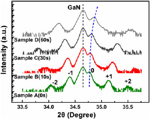
Various interruption time were used to modify both the G/A and A/G interfaces of the GaN/AlGaN heterostructures, and the structural information of sample A–D was measured by XRD ω-2θ scans of the symmetrical (0002) Bragg reflection, as shown in Fig. 2. For the control sample, A, the pattern shows the GaN main peak at 34.6° and the clear superlattice-related satellite peaks of the −2 to +2 orders, indicating a considerably good quality of the superlattices structures. With theoretical rocking curve simulation, the Al content of the AlGaN barrier layer is determined to be about 0.4, consistent well with our design. As the interruption time increases, one can see that the 0th satellite of the superlattices shifts discretely away from the GaN main peak to higher 2θ degree, indicated by the dashed line in Fig. 2, and the separation between the adjacent satellites becomes wider. At the beginning of our design, it was expected that an optimal interruption time should exist best improving the interface abruptness and then leading to the sharper and more clear satellite peaks. However, in fact, we did not observe that optimal point. Instead, the results show that with longer interruption treatment, the satellites become weaker and broader, which indicates a worse interface quality. When the interruption reaches 60 s (sample D), only the satellites of the −1, 0, and +1 orders are visible and the +1 order satellite becomes a broad hump. This suggests that the interface condition and interruption effect with NH3 flow would be much more complicated than reported,Reference Li, Aoki, Katsuno, Miyake, Hiramatsu and Shibata 19 in which the XRD results showed the improvement of interface quality by growth interruption. To clarify the reaction process at the interfaces, it is necessary to elucidate the effect of NH3flow on the (Al)GaN surface.
(0002) XRD ω-2θ scan for the GaN/AlGaN superlattices samples with different growth interruption treatments between the well and barrier layers (samples A–D). With interruption time increasing, the 0th satellite shifts gradually away from the GaN main peak to higher 2θ, indicating the increase of average Al content in the superlattices.

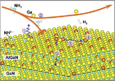
Figure 3 shows the schematic of the possible reactions and processes taking place on the (Al)GaN surface during the growth interruption with pure NH3 flow at high temperature. The following processes may happen on the (Al)GaN surface: (1) decomposition and evaporation of Ga atoms from the surface at 1050 °C, which is also called as “the etching effect”Reference Bai, Wang, Parbrook, Ross and Cullis 20 ; (2) the evaporated Ga atoms are taken away by gas flow, which can lead to the interface roughness and the reduction of the layer thickness; (3) Al–N molecules escape from the on-site binding and migrate around to seek a energetically more stable site, smoothening the surface geometryReference Li, Aoki, Katsuno, Miyake, Hiramatsu and Shibata 19 , Reference Schupp, Lischka and As 21 ; (4) recapture of the migrating Al–N molecules by the surface vacancy, reforming of AlGaN epilayer; and (5) downward diffusion of metal atoms (Al or Ga) across the interface. Thus, the effect of the growth interruption and the interface quality would strongly depend on which process mentioned above may dominate. Generally, at the A/G interface, processes (3) and (4) may dominate, and at the G/A interface, processes (1) and (2) would play the key role. With this surface model, one is able to explain the microscopic reactions at the interfaces with different interruption treatments.
Process schematic during the growth interruption at the AlGaN interface with NH3 flow. (1) Decomposition and evaporation of Ga from AlGaN surface, (2) evaporated Ga atom taken away by flow, (3) surface diffusion of Al–N molecules, (4) recapture of diffusing Al–N by the surface, and (5) downward diffusion of metal atoms across the interface.

From Fig. 2, it is observed that the 0th satellite peak shifts to higher 2θ degree with increasing the interruption time. In principle, the distance between the 0th satellite and the GaN main peak directly reflects the average Al composition over the whole superlattices. Thus, in our samples, the shift of the 0th satellite peak represents the increasing of the average Al content due to the Ga decomposition and thickness reduction of the GaN well layer. This variation can be attributed to the domination of processes (1) and (2), which means that the longer interruption time may enhance the GaN layer decomposition at the G/A interface, and hence, the overall average Al content of the superlattices is relatively increased. On the other hand, as the interruption time increases, the interval distance between the adjacent satellites increases as well. With rocking curve simulation, one can know that the satellite separation is closely associated with the thickness of the period of well and barrier.Reference Wie, Chen, Kim, Liu, Choi and Hwang 22 In this regard, the increasing distance indicates that the thickness of the superlattice is reduced with the NH3 blowing. In our cases, the thickness reduction mainly occurs in the GaN well layer due to the high-temperature evaporation of GaN at the G/A interface. Under NH3 flow at 1050 °C, processes (1) and (2) may react faster than processes (3) and (4), and consequently, this results in a nonequilibrium process leading to the GaN reduction. Meanwhile, the interface roughness becomes worse also because of the “etching” effect. In principles, the migration and reformation of Al–N molecule on the surface in processes (3) and (4), under NH3flow, is believed to play a key role in making the A/G interface smooth and improving the abruptness. However, no clear clue was observed in these XRD rocking curves. Moreover, process (5) of cross-interface diffusion should also be critical in influencing the interface quality, while how the role of this process would act remains unclear. To further investigate these issues, the detailed study of the interfacial structures with growth interruption was carried out using transmission electron microscopy (TEM).
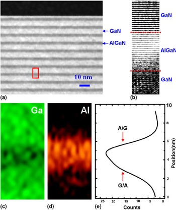
Figure 4(a) displays the STEM image of GaN/AlGaN superlattices of sample B (10 s/10 s). As we know, by the HAADF-STEM method, the image contrast is approximately proportional to the square of atomic number (Z2). Thus, one can see that the bright and dark stripes in Fig. 4(a) directly correspond to the GaN wells and the AlGaN barriers, respectively. In detail, the thicknesses of each AlGaN and GaN layer measured from the image are about 3.2 and 4.7 nm, respectively. Since the well and barrier can be clearly distinguished, it seems that the heterointerfaces should be abrupt. However, when we look into the local geometry of the G/A and A/G carefully, it is observed that the interface condition appears surprisingly much more complicated than what we expected. From the bright-field HRTEM image of the G/A and A/G [Fig. 4(b)], one can see that the A/G is visibly abrupt, whereas at the G/A, the presence of a narrow region in gray contrast can be seen. Considering the mass contrast of HRTEM, this gray region could illustrate the gradient diffusion of Al downward from AlGaN layer into the GaN layer. To confirm this phenomenon, the elemental mapping for Ga and Al of the area covering the G/A and A/G, marked with a red box in Fig. 4(a), was carried out with STEM, as shown in Figs. 4(c) and 4(d). Two interfaces can be identified, and the G/A reflects some diffusion of Al around the interfacial layers. Detailed examination with quantitative line scan of Al composition through two interfaces was made to determine the elemental abruptness of the heterointerfaces, as shown in Fig. 4(e). One can see that the transition of Al content at the A/G and G/A shows obviously asymmetric slopes. By using the 30–70% criterion,Reference Prosa, Clifton, Zhong, Tyagi, Shivaraman, DenBaars, Nakamura and Speck 23 it is determined that the A/G appears a steeper transition with the interface abruptness of about 0.71 nm, whereas the G/A demonstrates a gradual transition from AlGaN to GaN where the diffusion of Al covers a depth of about 1.16 nm. Although the accuracy of elemental resolution by STEM is limited, these trends still reflect the fact of the distinctly asymmetric abruptness of these two different interfaces, which can be explained by following analysis. As we know, Al adatoms are sticky to the surface and have much lower surface mobility than Ga adatoms.Reference Hawkridge, Liliental-Weber, Kim, Choi, Yoo, Ryou and Dupuis 24 Hence, the A/G would require longer growth interruption time for the migration of Al adatoms, approaching a better smoothness of the interface. Furthermore, an interruption duration is essential at the A/G for the removal of the residual flux of TMAl by NH3flow, avoiding the incorporation of Al into the subsequently growing GaN layer. On the contrary, at the G/A, the GaN layer turns to evaporate at high temperature during the growth interruption. This will lead to interface roughness and also create vacancies on the surface and after the interruption, supply of Al atoms easily cooperate into the vacancies, and the downward diffusion [process (5)] into GaN layer takes place in the meantime. That is why the gradient diffusion region appears at the G/A interface.
TEM images of GaN/AlGaN superlattices structure of sample B: (a) cross-sectional HAADF-STEM image. The GaN and AlGaN layers can be clearly identified. (b) Close-up HRTEM image of the G/A and A/G. An asymmetry for these two interfaces is observed after growth interruption treatment. (c) The elemental mapping for Ga and (d) Al of the area covering G/A and A/G. (e) Line scan of Al composition through the G/A and A/G. The significant Al diffusion at the G/A is the main reason for breaking the interfacial abruptness.

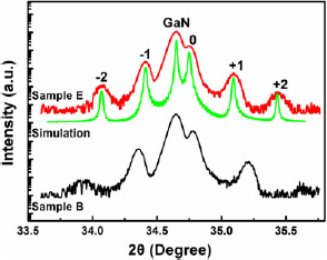
Based on the above analysis, one must realize that due to the different features at the G/A and A/G, using the same interruption treatment would be inappropriate for the interface improvement. Thus, an alternative interruption scheme is proposed here for optimizing the condition of different interfaces accordingly. On this purpose, the interfaces of sample E were modified with an interruption for 10 and 0 s at the A/G and G/A, respectively. Figure 5 shows the XRD rocking curve of sample E compared with that of sample B. It can be clearly seen that the superlattices-related satellite peaks of sample E become clearer and sharper than that of sample B. Especially, for the high-order satellites (−2 and +2 order), the intensity is significantly enhanced and the full-width at half-maximum (FWHM) appears slightly narrower. Most importantly, with theoretical simulation, we find that the well and barrier width obtained from the satellite separation in sample E is kept very close to that of sample A (Fig. 2). In addition, the elemental profile of Al for sample E by using Auger electron spectroscopy showed that the interfacial abruptness has been less than 1 nm for both interfaces. These confirm our previous assumption that the predominant evaporation reaction of GaN at the G/A with long interruption will reduce the GaN well thickness. Thus, the alternative interruption technique removes the interruption at the G/A and hence avoids the unnecessary consumption of GaN layers and surface roughening. Meanwhile, the abruptness of the A/G is improved with a 10-s interruption due to the Al migration enhancement, which is also important for the enhancement of the carrier confinement within the GaN quantum well.
(0002) ω-2θ scan of the GaN/AlGaN superlattices for samples E and B. The obvious improvement of the interfacial abruptness in sample E is achieved with the alternative interruption scheme (10 s/0 s), compared to that to sample B (10 s/10 s).

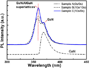
PL measurements were carried out to investigate the variation of optical properties with different interruption schemes, as shown in Fig. 6. The peak at the longer wave length is related to the band edge emission of the GaN template layer, which is assigned with the spectrum from the GaN epilayer. Hence, the peak at the shorter wave length is attributed to the PL emission from the superlattices. The superlattices peak from sample E has been significantly enhanced by about 39%, compared to that of sample B, though the GaN peak remains unchanged. It can also be seen that the FWHM of the superlattices peak in sample E decreases greatly. These results directly reflect the improvement of the abruptness of the heterointerfaces in the GaN/AlGaN superlattices. The short-time growth interruption used at the A/G seems critical in increasing the interface abruptness because the Al adatoms could have enough time to migrate to the more stable sites and the residual flux of TMAl will be carried away by the NH3 blow as well. On the contrary, continuous growth method is more helpful for preserving the smoothness of the G/A. On the other hand, it can be found that the obvious blueshifts of the superlattices peaks occur in sample B, which, actually, is associated with the reduced well width induced by the G/A interruption, as aforementioned. As we know, the width reduction of well layer may enhance the quantum confinement effect therein and consequently leads to the blueshift.Reference Vinciguerra, Franzo, Priolo, Iacona and Spinella 25 In contrast, with the alternative interruption scheme used in sample E, the blueshift of the superlattices peak stemming from growth interruption has been well eliminated, in good alignment with that of sample A.
Room temperature PL spectra of GaN/AlGaN superlattices samples E, A, and B, grown with different interruption schemes. It shows that the alternative interruption at the G/A and A/G of GaN by 10 and 0 s leads to the enhancement of superlattices-related emission. The spectrum of GaN underlayer was measured to assign the GaN peak.

IV. CONCLUSIONS
In conclusion, the interface abruptness of GaN/AlGaN superlattices in various growth interruption conditions has been studied and the complicated reactions with NH3 flow during the interruption were clarified. We found that the quality of the heterointerfaces highly depends on the duration of the growth interruption. With interruption time increasing, the XRD rocking curves showed that the 0th satellite of the superlattices shifts gradually toward higher 2θ degree and the interval distance between the adjacent satellites becomes larger. This indicates the increase of the average Al composition in the superlattices and the reduction of the well thickness due to the evaporation of GaN. Investigations with HRTEM and STEM revealed that an asymmetric abruptness appears at the G/A and A/G of the GaN/AlGaN heterostructures, suggesting the negative influence of interruption treatment on the G/A interface. An alternative interruption scheme was proposed to improve the interface quality with specific interruption for different interfaces. It was found that the (10 s/0 s) interruption for the A/G and G/A could lead to the best abrupt interfaces with sharp XRD satellite peaks, and the light emission efficiency from the superlattices was significantly enhanced due to the stronger quantum confinement. This alternative interface–interruption scheme provides an interface control method for obtaining symmetrically abrupt heterointerfaces and can be a point of reference for future research in high Al-content AlGaN-based heterostructures.
ACKNOWLEDGMENTS
This work was partly supported by the “973” programs (Grant Nos. 2012CB619301 and 2011CB925600) and “863” (Grant No. 2011AA03A111), the FRFCU (Grant Nos. 2012121011 and 2011121042), the National Natural Science Foundation, and Science & technology program of Fujian and Xiamen of China.