I. INTRODUCTION
The vapor–liquid–solid (VLS) process is typically associated with directional growth of semiconductor whiskers and nanowires. Its basic mechanism has been understood for quite some timeReference Wagner and Levitt1, Reference Givargizov2; yet continued scientific and technological interest in growth of one-dimensional (1D) structures has lead to a range of intriguing findings, theoretically and experimentally. Regarding the scope of this article, it is worth mentioning the recent theoretical work on the shape evolution of VLS-grown nanowires, which is controlled by the action of surface and line energies.Reference Givargizov2–Reference Li, Tan and Gösele4 On the experimental side, growth of very thin silicon oxide strands from liquid gallium implies that a wide range of 1D materials with different morphologies can be grown via the VLS mechanism.Reference Pan, Dai, Beach and Lowndes5, Reference Zheng, Wu, Yang and Liu6
In contrast to crystalline semiconducting nanowires grown by the conventional VLS process, silicon oxide nanostrands are amorphous and have a significantly smaller diameter than the growth mediating liquid droplet, which is often gallium, indium, or even tin.Reference Pan, Dai, Beach and Lowndes5–Reference Bettge, MacLaren, Burdin, Wen, Abraham, Petrov and Sammann9 However, the most striking feature is the emission of multiple long, exceptionally thin precipitates that tangle together like a yarn made from fine threads or like a stranded cable or wire made of multiple strands. The latter inspires the terminology, borrowed from electrical engineering, that we use throughout this study: “wire” for a bundle and “strand” for an individual fiber.
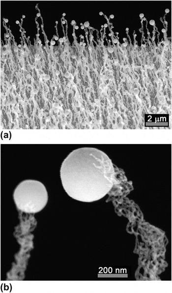
In a previous publication,Reference Bettge, MacLaren, Burdin, Wen, Abraham, Petrov and Sammann9 we described a method to fabricate arrays of aligned and freestanding silica nanowires over large areas (Fig. 1). Fabrication temperatures remain below 200 °C, and no lithography or other templating methods are used. Our process is based on reactive magnetron sputtering, performed in an atmosphere containing argon and water vapor. Sputtering supplies a concurrent flux of neutral Si atoms and energetic ions to a seed layer of indium droplets on the substrate. Indium acts as the liquid growth mediator for the VLS mechanism, held in the liquid phase throughout growth by heat supplied from the substrate heater, the sputtering process at the magnetron, and the substrate bias that accelerates ions toward the substrate. Details about the process are featured elsewhere.Reference Bettge, MacLaren, Burdin, Wen, Abraham, Petrov and Sammann9 Key characteristics of this relatively new process are the use of low melting temperature and low surface energy indium, and directional ion bombardment promoting oriented nanowire growth. For example, exposure of stranded silica nanowires to directional ion irradiation at 30 keV plastically deforms the nanowires in such a way that they bend into the incident ion beam. At a sufficiently high dose, the nanowire axis is completely aligned with the incident ion beam (Publication in preparation).
Arrays of stranded silica nanowires after their ion-enhanced vapor–liquid–solid growth. (a) Scanning electron microscopy (SEM) image showing such an array at a tilt view angle of 55°. The nanowires are vertically oriented. (b) Two stranded nanowires terminated by individual indium droplets revealing their internal structure: multiple entangled nanostrands connected to the droplet.

Individual silica wires are vertically oriented with a height of up to several micrometers. Their stranded internal structure is clearly visible (Fig. 1). A loose bundle of nanoscale strands forms a single “stranded” oxide nanowire that is connected to the substrate and terminated by an indium droplet at the tip. The indium droplet mediates the VLS growth of the individual oxide strands, and as they continuously precipitate from the droplet, they entangle and eventually form the stranded wire. Under continued energetic ion irradiation from any direction, the stranded wires become less porous and align themselves with the axis of the ion flux to within a few degrees. The same mechanism accounts for the generally vertical orientations of the wires in response to the modest ion flux along the substrate normal throughout growth. The diameters of individual strands close to the droplet are 9 nm or less, and are remarkably independent of the droplet diameter. The ratio of wire diameter to droplet diameter is only ∼0.01.
In this article, we intend to shed some light on the origin of the peculiar differences between liquid indium-mediated growth of stranded silica wires and “conventional” crystalline VLS wire growth. The origin of these differences can be found at the three-phase line (TPL), where a relatively large liquid–solid (LS) interfacial tension together with a small but essential line tension simultaneously affects precipitation of individual silica nanostrands.
II. FORCE BALANCE ANALYSIS
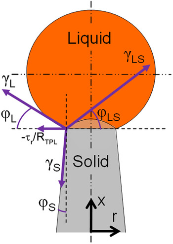
We begin with a general force balance analysis at the TPL considering a spherically capped fiber in axisymmetric contact with a spherical droplet. Mechanical equilibrium is established if the interfacial forces (per unit length) at the TPL are balanced, as depicted in Fig. 2.
Planar representation of the interfacial and line forces acting at the three-phase line (TPL) of a droplet-fiber system. The force due to line tension is shown in reverse for improved clarity. At steady state growth, φS = 0.

This yields the Neumann quadrilateral relation that is the extended Neumann triangle relation in the presence of a line tension (or line energy as it is sometimes termed).Reference Neumann and Jan10 Its axial (x) and radial (r) components are described in Eqs. [1(a) and 1(b)], respectively.

where γ refers to the involved surface or interfacial tension, and the subscripts L, S, and LS refer to the liquid–vapor, solid–vapor and liquid–solid interfaces, respectively. In addition, R TPL is the radius of the TPL, and τ is the line tension that is assumed to be constant.Reference Schmidt, Senz and Gösele11–Reference Sivaramakrishnan, Wen, Scarpelli, Pierce and Zuo13 Its force contribution, τr/R TPL, acts at the TPL and scales with the TPL curvature, becoming more important as the radius approaches nanoscale. Its normal force component, if positive, is inward along the radial direction. Rotational symmetry around the x-axis is assumed. All interfacial tensions (γ) are positive, and φ L ≥ 0° must hold so that the droplet remains a sphere. We assume isotropic surface energies, independent of curvature, and constant droplet volume. We also neglect any effects of solute and impurity concentrations on the relevant surface energy terms. The particular nature of the indium–silica droplet-strand system greatly simplifies the analysis because no crystal phases are present and because the indium droplet can be two orders of magnitude larger than the individual silica nanostrands. We choose to ignore any complications that result from the tangling of the strands as they leave the droplet, recognizing that the analysis is intractable without the assumptions of axisymmetry, an absence of external forces, and near equilibrium growth conditions. Clearly, these assumptions are only an approximation to reality. The tangled nature of the growth is not explained by the model. Nor does it offer any way to account for disturbances due to ion bombardment, so we can offer no insight regarding the possible effects of ion impact near the TPL. Nevertheless, we note that the strand radii we see are quite similar to those obtained without sputtering,Reference Pan, Dai, Beach and Lowndes5 suggesting that the fundamental processes are not substantially altered by bombardment.
At steady state, the radii of fiber, liquid droplet, and TPL remain constant during growth. Thus, φ S = 0, R TPL = R wire, τx = 0, and based on the geometry in Fig. 2, sin(φ L) = (R wire/R drop), so  where R wire is the fiber radius and R drop is the droplet radius (for φ L < 90°). The Neumann quadrilateral relation is then simplified to:

For any given geometry, we may define an effective interfacial energy  and an effective contact angle
 of the LS interface so that
 and
 We can thus obtain a straightforward equation describing the ratio of the two radii (R wire/R drop) from Eqs. [2(a) and 2(b)], using the trigonometric identity cos2(φ L) + sin2(φ L) = 1 to eliminate φ LS:

Obviously, a physical solution for axial growth can only exist for 0 < Φ < 1. Precipitation of silica nanostrands yields a very small radii ratio, Φ ∼0.01. For comparison, the ratio for conventionally grown germanium or silicon nanowires via gold is much larger—typically around 0.8–0.9.Reference Kodambaka, Tersoff, Reuter and Ross14, Reference Kodambaka, Tersoff, Reuter and Ross15 At the lower limit where Φ approaches zero, several conditions must be satisfied for stable growth based on Eqs. [2(a) and 2(b)]:

This means that the effective LS interfacial energy  must be the dominant energy term in the three-phase system, and that the LS interface must be convex, penetrating the droplet. In addition, φ L ≤ 90°, because an angle equal or larger than 90° would not satisfy mechanical equilibrium. The line tension τr can theoretically take on both positive and negative signs. An extensive discussion on the nature of line tension is provided elsewhere.Reference Amirfazli and Neumann12 However, there are important differences between a positive and a negative line tension on fiber growth when Φ is small. If the line tension is positive (i.e., its force contribution at the TPL points radially inward), a small perturbation reducing the fiber diameter at the TPL would increase its force contribution. This would require φ S to become negative to effectively re-establish the force balance and would thus result in inwardly tapered growth, and possibly fiber pinch-off. A similar argument holds that a small perturbation increasing the wire diameter would cause outward tapering of the fiber. Overall, fiber growth would be unstable because of this positive feedback mechanism. A stabilizing negative feedback can only be effectively established if the line tension is negative (i.e., its force contribution points at the TPL radially outward). In this case, a small perturbation reducing the fiber radius at the TPL would decrease its force contribution, which can be readily satisfied with φ S becoming positive. This suggests that the line tension must always be negative for stable growth, at the limit of small Φ.
With some additional manipulation, we find an analytical expression for the line tension. Solving Eq. [2(a)] for φ LS and applying the trigonometric identity cos2(φ L) + sin2(φ L) = 1, we obtain  , which, when substituted into Eq. [2(b)], yields

Eq. (5) describes the line tension contribution, τr/R TPL, only in terms of the interfacial energies and the ratio of the radii.
III. ESTIMATION OF INTERFACIAL AND LINE ENERGIES
With this basic understanding, we now seek to estimate the LS interfacial and line energies of fine silica strands in contact with liquid indium droplets. Although the surface energy of liquid indium is known to be ∼560 mJ-m−2 at its melting point,Reference Lang and Haynes16 the interfacial energy of the indium–silica LS interface and the surface energy of solid silica are not readily available from the open literature, making direct calculation of the line tension impossible using the equations derived above.
We solve this impasse in two steps. First, we use literature data from a mix of experiments, including two different geometries (“droplet-on-wire” and “droplet-on-plane”) and two different materials systems (gallium–silica and indium–silica) to evaluate the surface energy of silica and the indium–silica LS interfacial energy. The second step may then proceed in two ways: We may either directly apply the results of step one to Eq. (5) to obtain the line tension, given typical observations of droplet and strand size from our experiments, or we may apply our entire data set of strand and droplet sizes to Eq. (5), and allow the LS interfacial energy and the line tension to be adjusted for best fit to the data. This second method provides a better insight into the effects of both the LS interfacial energy and the line tension on the relationship between droplet and strand sizes, whereas the first method gives a more direct result.
The first step begins with the results of Naidich and Chuvashov,Reference Naidich and Chuvashov17 who compared the wettability of pure gallium and indium-rich (65 at.%) gallium droplets on a planar silica substrate and found only minor differences between the two equilibrium contact angles. We can consequently estimate the contact angle of pure indium on silica to be very close to that of the indium-rich gallium alloy on silica at the same temperature, i.e., about 126°. This angle can be used in Young’s equation for an indium droplet on planar silica to establish the direct relationship between γ S of silica and γ LS of indium–silica. As the indium–silica system is too rarely studied to allow us to get any data on γ LS of indium–silica, we consider related interfacial studies involving silica to obtain its solid surface energy. For example, liquid gallium in contact with silica has been explored in two different studies with two different geometries: (i) the wettability of pure gallium in contact with planar silica was studied by Naidich and Chuvashov,Reference Naidich and Chuvashov17 as mentioned previously; (ii) Pan et al.Reference Pan, Dai, Beach and Lowndes5 reported stable growth of amorphous substoichiometric silica nanostrands from liquid gallium droplets. Contact angle and γ L for liquid gallium on planar silica are known to be 128° and ∼710 mJ-m−2, respectively.Reference Lang and Haynes16, Reference Naidich and Chuvashov17 The combined application of Young’s equation with Eq. (3) for gallium in contact with silica eliminates the one unknown parameter, γ LS of gallium/silica, and leads to a unique solution for the surface energy of silica, γ S≈350 mJ-m−2. For Eq. 3 to be applicable, the ratio of the radii must be known. Those are provided in Pan’s work: The silica strand radius is ∼30 nm; the gallium droplet radius is ∼1750 nm.6 With γ S known, we can also calculate γ LS for the Ga-silica droplet-nanowire system which is ∼785 mJ-m−2. In this case, φ LS of the Ga-silica interface is +24°. The above steps are also outlined in the Appendix. The obtained γ S value falls well within the range of reported surface energies for silica (200–550 mJ-m−2).Reference Livey and Murray18–Reference Harding and Rossington20 With γ S finally determined, we can now solve Young’s equation for γ LS of the indium–silica system. We obtain γ LS,indium–silica≈680 mJ-m−2. It is worth noting that solving the surface energies for gallium in two different geometric arrangements provides a unique solution for γ LS, circumventing what is typically a major challenge for surface tension measurements.
We assume that γ S is the same in all three studies, i.e., in ours, Naidich’s and Pan’s. We also presume the LS interfacial energies for each material system are invariant between the two geometries studied. Furthermore, the line tension contribution, τr/R TPL, on strands grown by gallium in Pan’s work is small. Assuming the line tension τr is comparable for In– and Ga–grown nanostrands, its effect must be approximately one order of magnitude smaller in Pan’s experiments than in our own, due to his larger TPL radius.Reference Pan, Dai, Beach and Lowndes5 The effect of the line tension in Naidich’s work can also be neglected because of large droplet sizes.Reference Naidich and Chuvashov17
The line tension contribution for the indium–silica system can now be calculated according to Eqs. [2(a) and 2(b)] or Eq. (5). By using typical values for strand and droplet radii, 3 nm and 100 nm, respectively, we obtain a relatively small and negative value for the line tension contribution, τr/R TPL = −33 mJ-m−2. The magnitude of the line tension τr is thus −1 × 10⁻¹⁰ J-m−1. Also, the LS interface penetrates into the droplet at φ LS = +29°. This is in agreement with the theoretical requirements outlined earlier. It is also important to recognize that Eq. (5) cannot be satisfied in the absence of the line tension contribution by using the derived interfacial energies alone. That is, VLS growth of fine silica strands from a large indium droplet is impossible without the influence of line tension.
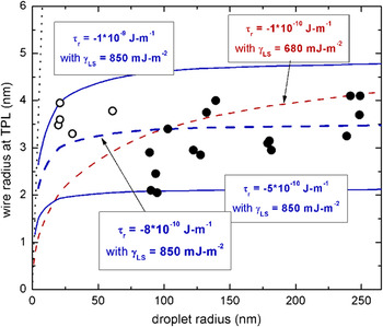
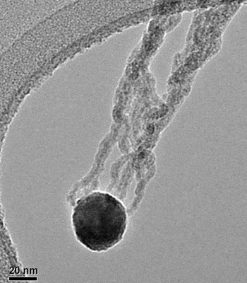
In the absence of a line tension, a linear relationship between strand radius and droplet radius through the origin is required for steady state growth according to Eq. (2), since τr = 0 and φ S = 0. Our experimental data deviate significantly from this relationship, as shown in Fig. 3, where strand radii are plotted against the radius of the droplet to which they are attached. The sizes of the indium droplets and the corresponding nanostrands were measured by high-resolution scanning electron microscopy (Hitachi 4800, Hitachi High Technologies America, Inc., Pleasanton, CA) and transmission electron microscopy (TEM; JEOL 2010F, Japan Electron Optics Laboratory, Tokyo, Japan). A typical TEM image of a droplet with several strands is shown in Fig. 4, illustrating issues that arise for both scanning electron microscopy (SEM) and TEM data acquisition. Strands overlap through much of each image, so the strand diameter is estimated from the minimum apparent width of the growth for each strand close to the droplet. Clearly obstructed strands are ignored. The average standard deviation of the strand radii is 0.4 nm.
Nanostrand radius at the TPL as a function of the indium droplet radius at stable growth conditions. Solid and empty circles show measurements using SEM and transmission electron microscopy (TEM), respectively. The displayed data on the abscissa are average radii of strands precipitated from a single droplet. The dashed and solid curves represent least squares fits that are obtained using the line and interfacial energies indicated. The two solid curves represent solutions of Eqs. [2(a) and 2(b)] for the minimum and maximum line tension required to envelop this data set. The red dashed curve represents, for comparison, the radius function for the line tension and liquid–solid interfacial energies derived for Φ = 0.03, chosen from the data element with 100-nm droplet radius. The position of Φ = 0.8, typical of the gold–silicon VLS system, is represented for comparison by the dotted black line close to the left hand side of this figure.

TEM image of several strands emitted from one indium droplet. Distinct and unobstructed strands are often found in close proximity of the droplet.

Since both radii are readily measureable, Eq. (5) can be used to numerically fit γ LS and τr to the experimental distribution of strand radii as a function of the droplet radius. This is our second approach that additionally allows us to verify the interfacial energy and line tension quantities obtained with the first approach.
As shown in Fig. 3, a good fit is obtained by presuming a negative line tension. A least squares fit of the entire data set yields γ LS,indium–silica = 850 mJ-m−2 and τr = −8 × 10⁻¹⁰ J-m−2, represented by the dashed blue curve. This line tension gives rise to a significant force at the TPL (−266 mJ-m−2 for a TPL with a 3-nm radius). The least squares fit is in good agreement with the trend that uses the LS interfacial energy and line tension derived in the first approach, displayed as the dashed red curve for comparison. The two solid blue curves envelop the data and provide limiting values for the line tension for this data set. All of these curves were computed using γ L and γ S fixed at 560 and 350 mJ-m−2, respectively. The dotted black curve on the left hand side of Fig. 3 goes through the origin and represents the predicted linear behavior in the absence of any line tension with Φ = 0.8, which is a common value for gold mediated VLS growth of crystalline semiconductor wires.
Exact measurements of the line tension are experimentally challenging. Our experimental line tension values fall, however, within one order of magnitude of each other, and are consistently negative and are on the order of −1 nJ-m−1. This magnitude is reasonable following the analysis proposed by Marmur which considered the line tension of a spherical droplet on a planar surface assuming only van-der-Waals interactions.Reference Amirfazli and Neumann12, Reference Marmur21 Using Marmur’s approach, the estimated line tension is around –4 × 10⁻¹⁰ J-m−1, assuming that the average spacing of the liquid and solid atoms is on the order of the liquid indium atom (∼0.3 nm). Also in another relevant study, Schmidt et al. reported a line tension value of ∼−10−9 J-m−1 in their growth of crystalline silicon nanowires.Reference Schmidt, Senz and Gösele11
In comparison to conventional VLS growth of semiconducting crystalline nanowires, it is somewhat surprising that continuous and stable growth of silica nanostrands <9 nm in diameter is in fact possible using a plasma-assisted, low-temperature VLS growth technique.Reference Bettge, MacLaren, Burdin, Wen, Abraham, Petrov and Sammann9 Bombardment with energetic particles and shadowing effects should cause an unsteady supply of reactants through the liquid indium, whereas mechanical tangling of the wires must also perturb steady growth. Yet the presence of a negative line tension provides the necessary negative feedback to maintain stable growth of such small diameter strands, independent of the size of the indium droplet.
IV. CONCLUSIONS
In summary, the force balance at the TPL is analyzed for VLS growth of small diameter silica nanostrands using liquid indium droplets. It is found that the contributions from a relatively large LS interfacial tension and a negative line tension at the TPL control and define stable growth of very small diameter strands. Their diameters are typically <9 nm, 100 times smaller than the indium droplet. As a consequence, a bundle of very fine, yet stable, nanostrands is precipitated out from a single indium droplet, forming essentially a stranded nanowire. The magnitudes of the relevant interfacial energies and of the line tension are determined from experimental data using two different approaches. The magnitude of the LS interfacial energy of indium–silica is on the order of 670–850 mJ-m−2; whereas the magnitude of the line tension lies in the range of −0.1 to −1.0 nJ-m−1.
We expect that this type of analysis can be applied to other materials systems and will enrich the ongoing discussion of surface and line energetics in general and their role during VLS wire growth in particular.
ACKNOWLEDGMENTS
The research was carried out in collaboration with Argonne National Laboratory (ANL) and in part in the Frederick Seitz Materials Research Laboratory Central Facilities, University of Illinois, which are partially supported by the U.S. Department of Energy under grants DE-FG02-07ER46453 and DE-FG02-07ER46471. Financial support was provided through ANL under Grant No. DOE ANL 1F-00861. We thank Changhui Lei for his help during TEM analysis.
APPENDIX
Calculation of the LS interfacial energy for the indium–silica droplet-strand system
The surface energies of liquid indium, γ L,In, and liquid gallium, γ L,Ga, are known, but no data are available for the interfacial energy in the indium–silica system, γ LS,In−silica, or for the surface energy of silica, γ S,silica. The latter can be obtained by using Young’s equation and Eq. (3) in combination for liquid gallium in contact with silica.
The use of Young’s equation with the known contact angle leaves two unknowns [Eq. (A1)]:

γ LS,Ga−silica can be obtained from Eq. (A2), which originates from Eq. (3) in the absence of any line tension contribution, i.e., τ r,Ga = 0.

The symbol Φ represents again the ratio of the two radii: Rwire/Rdroplet; also γ LS,Ga−silica is defined as a positive quantity. γ S,silica can then be calculated:

With γ S,silica known, γ LS,In−silica can now be obtained from Young’s equation [Eq. (A4)]. The contact angle is again provided in Naidich’s work.