Evaluation of the mechanical integrity of interfaces between thin coatings and substrates is a long-standing subject of interest in surface engineering and thin film mechanics, and a repeated topic of focused discussion within the last 20 years.[Reference Mittal1] As coating/substrate systems vary widely, from polymeric coatings on metallic substrates to hard ceramic coatings on ceramic substrates, a wide range of experimental methods have been conceived to test coating/substrate interfacial integrity. These methods include the pull and peel,[Reference Brown and Mittal2] scratch,[Reference Kattamis and Mittal3] indentation,[Reference Drory and Hutchinson4, Reference Vlassak, Drory and Nix5] tension,[Reference Agrawal and Raj6] and laser spallation[Reference Gupta, Kireev, Tian, Yoshida and Akahoshi7] tests.
Deposition of thin, hard, ceramic coatings has become an important method for engineering surfaces of mechanical components and manufacturing tools.[Reference Homberg and Matthews8] This class of applications are characterized by high contact stresses and high cycle loading, such as those experienced by ceramic coatings on cutting tools[Reference Zhang and Zhu9] and gears.[Reference Jiang, Meng, Evans and Cooper10] For the ceramic coating to survive such high-stress and high-cycle contact, the interface region between the coating and the substrate is so strong that pull and peel tests, in which auxiliary loading pads are attached by glues onto the coating surface,[Reference Brown and Mittal2] usually do not lead to the failure of the coating/substrate interface. Although scratch testing may yield relative rankings between different coatings on the same substrate at a fixed test geometry, its configuration is often too complex to allow a quantitative measure of interfacial mechanical properties.[Reference Bull and Mittal11]
Indentation tests with axisymmetric[Reference Drory and Hutchinson4] or long wedge[Reference Vlassak, Drory and Nix5] indenters have been performed on brittle ceramic coatings deposited on ductile substrates. In these tests, plastic deformation of the substrate caused by deep indents into the substrate exerts an additional in-plane compressive loading on the coating, leading to coating spallation away from the indent impression. The extent of coating spallation can be used to determine a value of the coating/substrate interfacial toughness. Such indentation tests have yielded quantitative toughness measures in coating/substrate systems with a relatively low interfacial toughness,[Reference Drory and Hutchinson4, Reference Vlassak, Drory and Nix5] and proved insufficient to cause a coating/substrate interfacial failure beyond the indent impression at higher interfacial toughness values.[Reference Wang, Sugimura, Evans and Tredway12] A full understanding of such indentation tests also requires a detailed elasto-plastic analysis which is dependent on the mechanical properties of the particular substrate being tested.[Reference Begley, Mumm, Evans and Hutchinson13]
In the tension test configuration, ductile substrates onto which brittle ceramic coatings are deposited are loaded in tension and deformed plastically. For thin coatings, the same strain is experienced by the coating and the substrate, with the substrate strain being plastic and the coating strain being elastic. This strain leads to transverse cracking in the coating perpendicular to the direction of tensile loading. Once transverse cracking occurs, tensile loading of the thin coating occurs through shear stresses at the coating/substrate interface region. The density of transverse cracks increases with increasing the substrate plastic strain to a plateau value, beyond which further increase in the substrate plastic strain does not cause additional decrease in crack spacing.[Reference Agrawal and Raj6] From the initial strain at which cracking develops, an apparent failure stress in tension is derived from the coating. By combining this apparent failure stress with the minimum spacing of transverse cracks in the coating at a large substrate strain, a limiting shear strength of the coating/substrate interface region is derived.[Reference Agrawal and Raj6, Reference Chen, Hwang, Yu and Huang14]
In laser spallation tests, a high-fluence laser pulse is directed toward the backside of the substrate, and sets up a compression pulse traveling toward the coating/substrate interface. Upon reflection at the interface, the pulse turns tensile. The magnitude of the tensile pulse may reach the interfacial tensile strength, in which case coating spallation is induced. From the critical laser fluence, a measure of the tensile strength of the coating/substrate interface is obtained.[Reference Gupta, Kireev, Tian, Yoshida and Akahoshi7]
Surface engineering of mechanical components and manufacturing tools by coatings often involves deposition of complex interfacial materials with the goal of promoting adhesion of thin hard coatings to the substrate.[Reference Jiang, Meng, Evans and Cooper10] A quantitative assessment of interfacial strength is desirable. While the tension test may yield a value for the limiting interfacial shear strength, it is indirect, subject to a large scatter, and is not conducive to yielding information on the critical material location/structure controlling interfacial failures.[Reference Mu, Chen, Lu, Meng and Doll15] While the laser spallation test has yielded quantitative measures of the interfacial tensile strength in simple cases, it places high demands on the back surface quality and the attenuation properties of the substrate, and may not be easily applied to cases of practical surface engineering interest. In the surface engineering and coatings field, a premium is therefore placed on effective testing protocols which can yield quantitative information on interfacial failure and be conducive to correlating interfacial chemistry and structure to interfacial failures. In this paper, we report a new testing protocol, in which inclined coating/substrate interfaces contained within microscale cylindrical pillars are failed by direct compression loading in the pillar axial direction. TiN coatings on Si substrates were used as an example to illustrate this protocol.
Deposition of TiN coatings was carried out at room temperature in an ultra-high-vacuum physical/chemical vapor deposition tool, which housed a 13.56 MHz inductively coupled plasma (ICP) and multiple balanced magnetron sputter sources.[Reference Mu, Chen, Lu, Meng and Doll15, Reference Meng, Curtis, Rehn and Baldo16] The sputter sources faced the center of the deposition chamber, with a base pressure of <3 × 10⁻⁹ Torr. Cleaned Si(100) substrates, 2 inches in diameter, were first placed into a load lock, evacuated to ≤3 × 10⁻⁷ Torr, and then transferred to a holder placed at the center of the deposition chamber. The substrates were rotated at ~12 rpm during deposition. Four pure Ti (99.99%) targets were operated in the dc current-controlled mode. The entire deposition sequence occurred in ~10 mTorr of Ar (99.999%+). The Si substrate was first subjected to an Ar ICP etch for ~5 min at a bias voltage of −50 V. Immediately after etching, an elemental Ti interlayer, ~200 nm in thickness, was deposited onto the substrate by sputtering the Ti targets in Ar with an ICP assist. Deposition of TiN coating layers, ~5 µm in thickness, occurred immediately after Ti interlayer deposition in an Ar/N2 (99.999%+) ICP. To ensure a reasonable deposition rate at close to stoichiometry, the input N2 flow was kept close to but below the pressure hysteresis point. During TiN deposition, a total input ICP power of 1000 W was applied and an electrical bias voltage of −30 V was applied to the substrate.
As-deposited TiN/Ti/Si(100) specimens were cut to pieces of smaller size. A stainless steel (SS) sheet metal, ~700 µm in thickness and cut to the same size, were bonded face to face to a TiN/Ti/Si(100) piece with M-Bond 610 adhesive. The bonded assembly was then embedded in commercial epoxy, with the TiN/Ti/Si interface pre-aligned with a 45° inclination to the epoxy top surface. After epoxy curing, its top surface was then polished by a SiC abrasive from 600 to 1200 grit, and finished with ~1 µm diamond suspension. Figure 1(a) shows an ion-induced secondary electron (ISE) image taken on an FEI Quanta3D FEG focused ion beam (FIB) instrument, which combines a field-emission electron source and a high-current Ga+ ion source. A thin Pt protection layer was deposited onto the mechanically polished specimen top surface via Ga+ catalyzed Pt metal–organic gas source deposition. The Ga+ beam was then used to mill into the specimen top surface to create a cross section, with the cross-sectional surface perpendicular to the specimen top surface. The ISE image in Fig. 1(a) shows the mechanically polished top specimen surface together with the Ga+ milled cross section into the specimen, with both the top surface and the cross-sectional surface labeled. The cross section was cut successively with Ga+ of reducing current from 50 to 0.1 nA, resulting in a smooth finish. The cross section reveals, in sequence from the left, the mating SS sheet metal, the M-Bond 610 layer, the ~5 µm TiN coating layer, the ~200 nm Ti interlayer, and the Si substrate. The TiN/Ti/Si interface was indeed oriented 45° to the top surface. The interface between the TiN coating and the Si substrate at the top surface is flat and smooth, without any polishing induced cracks.
Fabrication of micro-pillars containing inclined coating/substrate interfaces: (a) an ISE image of a polished TiN/Ti/Si(100) specimen. Both the polished top surface and an FIB cross section are visible and labeled accordingly; (b) a TiN/Ti/Si micro-pillar with a 45°-inclined interface. The schematic superimposed on the ISE image shows the creation of the micro-pillar by FIB milling.

As shown in the schematic superimposed on the ISE image in Fig. 1(a), microscale cylindrical pillars were milled from the polished assembly. In order to obtain micro-pillars without significant taper, a FIB script milling program was employed,[Reference Shade, Wheeler, Choi, Uchic, Dimiduk and Fraser17] enabling a lathe-like machining process with Ga+ ions. Figure 1(b) shows an example micro-pillar, with a diameter of ~3.85 µm, within which the TiN/Ti/Si interface is inclined 45° to the top surface. With the same method, other micro-pillars were fabricated from the same assembly, with diameters of ~5, ~4, ~3, ~2, and ~1 µm and at least 5 for each diameter. The minimum distance between the TiN/Ti/Si interface and the pillar top surface, in all cases, was ≥2 µm.
The compression loading of the TiN/Ti/Si micro-pillars was carried out at room temperature on a MTS NanoIndenter XP with a custom-made, ~10 µm × ~10 µm, flat-ended diamond punch. An increasing load was applied to the pillar top surface using displacement-controlled loading, with raw indenter load and displacement monitored continuously. Figure 2 shows the collection of measured raw load–displacement curves. It is evident from Fig. 2 that the raw data fall into 5 succinct groups, separated from each other according to the different pillar diameters. For each pillar, the load increased approximately linearly with increasing indenter displacement at the beginning. Then, the pillar failed abruptly when the load reached a breaking point, manifested in a large and abrupt displacement excursion: typically 4–5 µm. Although the loading program specified a displacement stop, set to 800 nm, the data shown in Fig. 2 indicate that the indenter failed to stop at the set point. The abrupt failure and the inertia of the indenter system led to total displacement excursions of 4–5 µm after failure. The unloading curves are thus largely irrelevant, and the main information contained within Fig. 2 is the load to failure. As is evident from Fig. 2, failure loads measured from separate pillars of similar diameters appear to exhibit good repeatability.
Load–displacement curves obtained from compression loading of TiN/Ti/Si micro-pillars with 45°-inclined interfaces. Data obtained from pillars of 5 different diameters are included, as indicated by the labels.
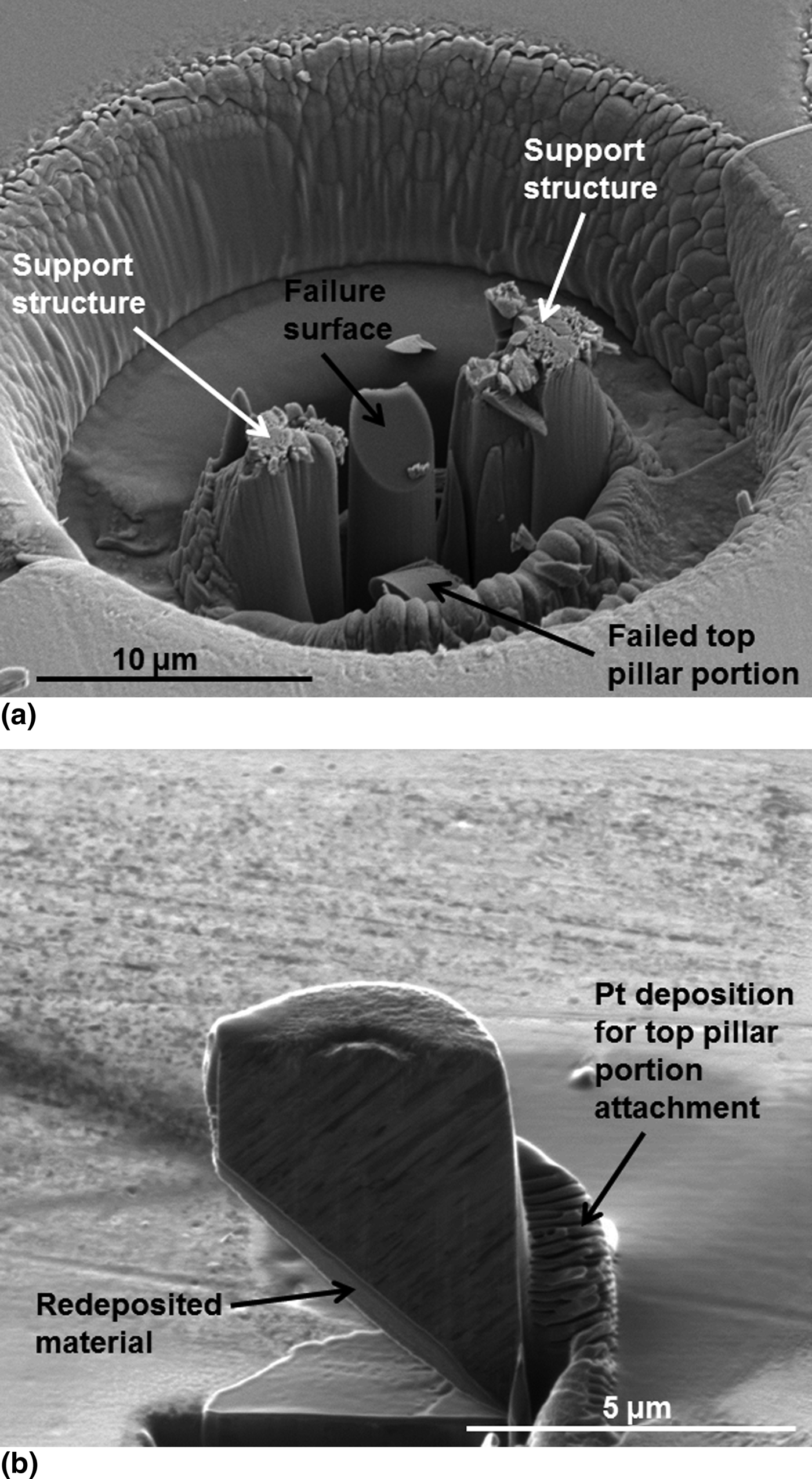
The large indenter displacement excursion associated with pillar failure led to the impact on what was beneath the indenter, typically destroying the remaining pillar specimen. This made detailed examination of the failure location difficult. In order to ascertain the physical location associated with pillar failure, on some pillar specimens, two support structures placed on two sides of the pillar were milled by the Ga+ ion beam. The height of the support structures were made to be lower than that of the pillar top surface. Such support structures did not influence the compression loading of the pillar by the indenter, but acted as a mechanical stop to the indenter when pillar failure occurred. Figure 3(a) shows the typical failure morphology of such supported TiN/Ti/Si micro-pillars. In Fig. 3(a), signs of indenter impact on the top of the support structures besides the pillar are evident. It is clear that the pillar failed in a 45°-inclined plane, parallel to the TiN/Ti/Si interface in the as-milled pillar. X-ray energy dispersive spectroscopy (EDS) data collected from the failure plane by electron excitation with incident beam direction parallel to the pillar axis showed signals of Si, Ti, and a minor O component. While O signals in the EDS data may result from brief exposures of the specimen to air, the presence of a Ti signal in EDS data collected from the failure plane suggests that the failure did not occur entirely within the Si substrate.
Failure of compression loaded TiN/Ti/Si micro-pillars: (a) failure morphology of one supported micro-pillar; (b) an ISE image of the FIB section of the failed top pillar portion.
As marked by one arrow in Fig. 3(a), the failed top portion of the original pillar is also evident, with a mating 45°-inclined failure plane. As shown in Fig. 3(b), this failed top pillar portion was picked up by an OmniProbe in situ the FIB instrument, and attached by Ga+ catalyzed Pt deposition to the specimen top surface in the vicinity of the crater shown in Fig. 3(a), with its axis aligned with the original direction. The purpose of this attachment is to allow ion beam sectioning of the failed top pillar portion to ascertain the location of the failure surface. The entire top pillar portion was then cut into half from the pillar top surface by Ga+ ions with incidence parallel to the pillar axis. Figure 3(b) shows an ISE image of the section, the majority of which exhibits a columnar structure with the column axes aligned parallel to the original growth direction, typical of polycrystalline TiN coatings deposited at low temperatures with ion-assist. Additional material was deposited below the failure surface due to sputter re-deposition during FIB sectioning. There exists a significant difference in contrast between the TiN layer and the redeposited material, which provides a clear delineation of the apparently smooth, 45°-inclined failure surface. Consider that the TiN top layer consists of randomly stacked nano columns, a smooth 45°-inclined failure surface is unlikely if the compression induced failure occurred entirely within the TiN layer. If failure did not occur entirely within the Si substrate or the TiN top layer, it is likely to have occurred in the Ti interlayer, or at the TiN/Ti or Ti/Si interfaces.
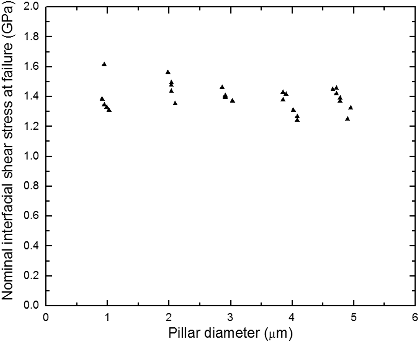
While TiN and Si are both expected to be brittle at room temperature, the Ti interlayer may exhibit some ductility. The raw axial failure load was therefore converted to a nominal interfacial shear stress at failure for 45°-inclined planes, τ = σ/2, where σ represents the raw failure load divided by the right cross-sectional area of the micro-pillar, i.e., σ is the axial failure stress in compression. Figure 4 shows values of τ as a function of the pillar diameter D. Since each data point in Fig. 4 represents an independent test on a separate pillar, the collection of data shown in Fig. 4 again illustrates good repeatability with the present test protocol. Averaged over all data points, τ is ~1.4 ± 0.1 GPa. The measured values of τ exhibited essentially no dependence on D over the range of pillars tested.
Values of the nominal interfacial shear stress at failure plotted as a function of the TiN/Ti/Si pillar diameter.
In an independent series of experiments, the limiting interfacial shear strength of TiN/Ti/steel interfaces was determined through the tension test method to be 1.5 ± 0.8 GPa.[Reference Mu, Chen, Lu, Meng and Doll15] Although the TiN/Ti/steel interfaces are not identical to those in the present experiments, they are related. The value of τ, 1.4 ± 0.1 GPa, presently determined for interfaces in the TiN/Ti/Si system through the micro-pillar compression tests, is very close to that of the previous tension test results conducted on TiN/Ti/steel interfaces. The observed lack of dependence of τ on D, together with imaging and EDS evidence suggest that compression induced pillar failure was located in the Ti interlayer, and suggests that the presently observed compression induced failures of the TiN/Ti/Si micro-pillars containing 45°-inclined interfaces may be related to plasticity within the Ti interlayer. Since the tension test is understood to be limited by interfacial shear, the closeness of the present τ values to previous tension test results does suggest that the present experimental results may not be out of line with plasticity events.
It is not possible with the present data to rule out the possibility that the compression induced failure of the interfacial regions of TiN/Ti/Si micro-pillars is fracture related. Taking a simple example of a cylindrical pillar of diameter D with a circumferential crack of length a loaded in tension, the stress intensity factor is given by K = Y(a/D)σa 1/2, in which σ is the remote loading stress and Y is a weak function of a/D.[Reference Hertzberg18] If failure occurs when K reaches the critical stress intensity factor K c, then the critical remote loading stress, σc = K c/(Y(a/D)a 1/2), may not exhibit a strong dependence on D if the crack length remains relatively constant as D varies. The observed lack of dependence of τ on D, shown in Fig. 4, does not therefore definitively exclude fracture as a possible failure mechanism. Even though the interface is loaded predominantly in mode II, a fracture mechanism may still be operative, including the possibility of fracture at the TiN/Ti or Ti/Si interfaces. A final determination of the predominant failure mechanism in compression induce failures of micro-pillars containing inclined interfaces requires additional studies, which are currently underway.
To our knowledge, the presently described protocol for testing coating/substrate interfacial failure through the direct compression loading of micro-pillars containing an inclined interface region is new. Large relative errors, ~50%, occur when the tension test[Reference Agrawal and Raj6] is used to determine the limiting interfacial shear strength in hard coatings with significant residual stresses.[Reference Mu, Chen, Lu, Meng and Doll15] In comparison, the present micro-pillar compression tests yield more reproducible failure stresses: typical data scatter at each pillar diameter is ~15%. While large and flat coating/substrate specimens are required for laser spallation tests, the present methodology can be used to fabricate a large number of micro-pillar test specimens from one relatively small sample. With scripted FIB milling, pillar fabrication can become automated and quite rapid. The failure surfaces can be made accessible to high-resolution structural and chemical analysis, and thus conducive to correlating the interfacial structure and the chemistry with mechanical failures within the interfacial region. Additional studies of coating/substrate interfacial failure using the presently described protocol are expected to contribute to further understanding and effective engineering of interfaces for enhanced coating performance, and are presently underway.
Acknowledgments
Partial project support from the NSF and LA BoR through grants CMMI-0556100 and CMMI-0900167 and contracts LEQSF(2011-13)-RD-B-03 and LEQSF(2011-13)-RD-B-04 is gratefully acknowledged. Additional support from NSF IIP-1058523 and IIP-1248353 through sub-awards to LSU is further acknowledged. KC and WJM acknowledge instructions from discussion with Dr. Paul Shade with respect to the FIB “lathe” milling program.