Scaling computation at constant cost, energy, and footprint
The deployment of new information technology must meet both performance and scalability specifications. Information hardware must conform to a common platform to leverage a common research, development, and manufacturing base. System architecture scaling has migrated from central processor units (CPUs) with ever-faster clock frequencies to increasing numbers of processors working in parallel with reduced clock frequencies. This fundamental architectural change resulted from the approach of power density limits as transistor switching voltages reached their scaling asymptote near 0.5 V. Parallel architectures scale linearly in power density with processor count, while continuation of clock frequency scaling at constant voltage would scale as the second or even third power of frequency (P = ½ CV 2f; P = power, C = capacitance, V = voltage, and f = frequency). Multiple processors working in parallel place an emphasis on fast and efficient inter-processor communication. Parallel, communication-centric architectures should ideally possess all-to-all connectivity with zero latency and energy. Software for massively parallel systems must adapt to minimal data movement or to detailed specification of data location and transport in the lines of code. Two vectors of convergence are active in creating scalable solutions for the next two decades: (1) electronic-photonic convergence to natively integrate communication into the computation process and (2) hardware-software-architecture convergence to provide intelligent, dynamic provisioning of energy-consuming computational resources. Microphotonic integration on the silicon platform embraces both vectors by utilizing the tools of silicon microelectronics and by supporting optimized complexity with novel electronic-photonic partitioning of functionality.1 This article presents the authors’ vision of the grand challenges for new materials, process integration, and foundry manufacturing platforms for scaling computation functionality.
Scaling computation architecture: A connectivity case study
The physics of information processing and transport dictates an ultimate tradeoff between clock/communication frequency and parallelism.Reference Agarwal2 While aggregate bandwidth must continue to scale at all levels of the interconnection hierarchy, the data rates of each channel must reach an asymptotic limit defined by the dissipated power density. Monolithic waveguide integration of optoelectronic devices with transport media, and high index contrast materials, which tightly confine light in dimensions of wavelength/refractive-index and allow for micron-dimensioned layouts, provide a path for scaling to small photonic devices coupled with low parasitic capacitance to electronic drivers and receivers.
Microprocessor performance is gated by two factors: communication bandwidth and programmability. Bandwidth is needed for low latency signal processing among the compute nodes without delays associated with contention and routing. As the number of cores (processors), N, grows exponentially with time, the desired communication bandwidth must grow as N Reference Agarwal2. Figure 1a shows a mesh interconnection solution, where data are transported by routing point-to-point between nearest-neighbor cores. The mesh architecture enables hundreds of cores to communicate with inexpensive local communication, before contention (blocking of a path while it is being used) and distance-dependent routing energy and latency become limits. However, the mesh introduces heterogeneity that increases programming complexity by requiring locality in the lines of code for point-to-point coordination of thousands of processes. Broadcast communication from one core to all other cores can relieve the need for locality in programming, but it is slow and power inefficient on an electrical mesh. A broadcast photonic network that allocates a unique wavelength of light to each sending core and an array of wavelength-selective receivers at each core (Figure 1b) can provide high bandwidth, low latency, and power-efficient communication among cores with no routing requirement by the hardware or data locality in the lines of code. This parallel architecture is known as ATAC: all-to-all computing.Reference Kurian, Miller, Psota, Eastep, Liu, Michel, Kimerling and Agarwal3,Reference Kurian, Chen, Chen, Miller, Michel, Lan, Antoniadis, Li-Shiuan, Kimerling, Stojanovic and Agarwal4
Scalable communication for multicore microprocessors. (a) Electrical mesh routing network for a 16 core microprocessor; (b) photonic all-to-all broadcast network.Reference Kurian, Miller, Psota, Eastep, Liu, Michel, Kimerling and Agarwal3,Reference Kurian, Chen, Chen, Miller, Michel, Lan, Antoniadis, Li-Shiuan, Kimerling, Stojanovic and Agarwal4 Note: m, local cache memory; p, processor; switch, to launch and route near-neighbor, core-core communication.

The ATAC architecture utilizes multichannel photonic waveguides that relieve both the bandwidth and loss limitations of the metal wire bus used in multicore microprocessors today. By allowing direct core-to-core communication, ATAC reduces the frequency of the memory calls implicit in the traditional bus architecture. Each off-chip memory read can consume 500 pJ of energy and 250 clock cycles, while a photonic network transfer consumes <3 pJ and <3 cycles. ATAC requires no routing, utilizes resources only when needed, and enables each core to directly communicate with any other core. A view of extended global memory can be efficiently enabled with an ATAC photonic network and distributed cache memory. Communication on the ATAC network is explicit and contention-free, encouraging the programmer to use it often with reduced overhead.
The ATAC architecture is likely to be used generically in complementary metal oxide semiconductor (CMOS)-integrated photonic circuits.Reference Kurian, Miller, Psota, Eastep, Liu, Michel, Kimerling and Agarwal3 Each core (node) is assigned a unique wavelength, and an optical power bus distributes all wavelengths around the chip. A sending core selects its wavelength through an optical filter (ring resonator), encodes it with data using an optical modulator, and launches it on an optical data waveguide for distribution to all other cores. If power-gated, monolithic lasers can be placed in each core, and additional advantages (∼50x) in energy efficiency can result. Each core has a filter/photodetector bank to independently drop each wavelength channel, to convert its data to electrical current, and to condition and process it as an electrical signal. This level of network complexity would be impossible with the discrete photonic components used in fiber optics, but waveguide integration provides the necessary small size and power efficiency.
Materials and devices for monolithic silicon microphotonics
Waveguide materials for high density optical interconnection
Two determining constraints for electronic and photonic integration on silicon are waveguides capable of (1) small bend radii that do not radiate transmitted light and (2) high transparency transmission. In silicon microphotonics, the silicon-on-insulator (SOI) platform has been widely employed, referred to here as the high index contrast (HiDex) platform, see Figure 2.Reference Lee, Lim, Agarwal, Wada and Kimerling5 A single mode Si waveguide, clad by SiO2 (n r = 1.5), confines light in small dimensions due to the high refractive index of silicon (n r = 3.5). For the telecommunication standard wavelength of 1550 nm, the single TE (transverse electric) mode silicon waveguide has dimensions of 200–250 nm thick and 400 nm wide for the HiDex platform. Doped-SiO2 fibers and planar lightwave circuits, here a low index contrast (LoDex) platform, where the typical index difference between core and cladding (Δn) is <0.1, possess a much larger 2–8 μm core thickness. HiDex materials typically have a larger temperature dependence of the refractive index (thermo-optic coefficient, TOC), which leads to a large fluctuation in channel wavelength in the wavelength division multiplexing (WDM) optical filters. The interchannel wavelength difference is 100 GHz (i.e., 0.8 nm at the 1550 nm range), which will soon reduce to 50 GHz. Thus, the fluctuation limits the maximum number of wavelength channels, because larger channel spacing is required to avoid signal overlap. In computing applications, the chip and package temperatures can fluctuate in operation from room temperature up to ∼70°C.Reference Hamann, Weger, Lacey, Hu, Bose, Cohen and Wakil6
Dimensional scaling for silicon photonics is dependent on the index difference (Δn) between the core and clad materials. SiO2 is the clad material for silicon photonics. The optical device footprint can be scaled smaller as the index contrast Δn increases; but device fabrication tolerances, such as waveguide sidewall roughness, become more demanding.
For high bandwidth communication, the HiDex silicon waveguide enables phase modulation by the injected carrier—plasma-induced change in index in one arm of a microphotonic Mach-Zhender interferometer (MZI). Therefore, the choice of material platform is application based: HiDex for active functions (photodetector, modulator, and light emitter) and LoDex for passive functions (such as WDM-MUX/DEMUX, wavelength division multiplexor/demultiplexor).
To accommodate small bend radii for waveguide integration on a chip of 1–2 cm2 area, the mid-index contrast (MiDex) materials platform (Figure 2) using silicon nitride (Si3N4) or silicon oxynitride (SiON) can offer advantages. Table I compares the behavior of thermally stable, ring resonators composed of Si3N4 and Si with a compensating polymer (negative TOC) cladding.Reference Raghunathan, Ye, Hu, Izuhara, Michel and Kimerling7 The composite materials waveguide structures give zero thermo-optic response. The smaller TOC of Si3N4 allows stronger confinement Γ in the waveguide core, and the effective index (n eff) and minimum ring bend radii (R b) are similar: Si3N4 (R b = 5.5 μm) and Si (R b = 3.5 μm). The stability and smaller intrinsic scattering loss (Figure 2) favor MiDex for on-chip dense wavelength division multiplexing (DWDM) applications in silicon photonics. Possibly the most significant advantage of the Si3N4 MiDex platform is its superior power handling capacity: two photon absorption at 1550 nm is negligible, and optical nonlinearity is more than one order of magnitude smaller than for Si. For example, scaling of the ATAC multicore DWDM application, described in the section on scaling computation architecture, is ultimately limited by the optical power in the signal bus waveguide: determined by the number of optical channels, the number of drop ports (N-1 receiver ports for each wavelength), and the drop power for each port (required for signal integrity at the employed data rate). If N is the number of nodes receiving the broadcast, then the required optical power in the waveguide is N Reference Agarwal2 x power/drop, which can exceed 1 W (∼1 GW/cm2 for Si) as the system architecture approaches >1000 nodes.
Polymer clad composite waveguide materials systems for thermally stable optical filters: zero resonant wavelength change between 0–70°C for Si and Si3N4 core materials.
Note: Core refractive index (n), optical mode confinement factor (Γ), effective index (n eff), group index (n g), and minimum bend radius (R b).Reference Raghunathan, Ye, Hu, Izuhara, Michel and Kimerling7
Device and process integration
The targeted implementation of silicon photonics is monolithic integration of optical circuits with electronic circuits in a “CMOS-like” standard process flow, as shown schematically in Figure 3.Reference Kimerling and Michel8 The historical path to monolithic integration began with discrete breadboards, then hybrid packages and chips, and finally monolithic integration. Current commercial products feature monolithic modulator-waveguide-detector integration with hybrid flip-chip bonding of the laser and electronics. The laser is the most difficult device to monolithically integrate on a silicon chip,Reference Soref and Lorenzo9 and III–V light emitters have been hybrid-integrated with transparent adhesives or wafer bonding in the back-end-of-line (BEOL).Reference Van Campenhout, Rojo-Romeo, Van Thourhout, Seassal, Regreny, Di Cioccio, Fedeli, Lagahe and Baets10,Reference Park, Fang, Kodama and Bowers11 Monolithic electronic-photonic integration in silicon microphotonics is expected to enable scaling of cost, manufacturing, energy, and bandwidth.
Schematic layout for monolithic integration of silicon photonic interconnection into the back-end-of-line (BEOL) complementary metal oxide semiconductor interconnect stack. This architecture is consistent with the size and function of photonics, and it can potentially simplify fabrication by eliminating interconnection layers.Reference Kimerling and Michel8 For the schematic structures, yellow represents the intralayer metal interconnects, gray is the interlayer metal interconnects, dark blue is the silicon transistor and optical waveguide elements, and light blue is the silicon wafer of the SOI layer. Note: SOI, silicon on insulator.
Silicon CMOS process technology is one of the most elaborate human-made resources in history. It provides the most accurate yet cost-effective processing for monolithic integration of electronics and photonics on a chip. The fundamental challenge for CMOS process technology for Si microphotonics is dimensional tolerance, because wavelength-dependent optical devices are more dimensionally sensitive than transistors. Fabrication errors in waveguide width/thickness as small as 1 nm can be consequential for on-chip DWDM. The absolute process tolerance of MiDex should be larger because of weaker confinement of light modes than in HiDex. The drawback of Si3N4 materials deposited by chemical vapor deposition is residual hydrogen in the film, leading to strong N–H bond absorption near 1520 nm,Reference Klunder, Tan, van der Veen, Bulthuis, Sengo, Docter, Hokstra and Driessen12 which is at the middle of the optical communication wavelength range. Annealing at 1100°C or higher is necessary to remove hydrogen from SiNx layers, and these temperatures are not tolerable in the CMOS BEOL processing. However, it should be noted that Si3N4 deposited by PVD is a compatible process that introduces no hydrogen.
Multiplexing for high aggregate bandwidth
Scaling interconnection to the highest bandwidth density will necessarily utilize DWDM, where 50 GHz (0.4 nm) channel spacing is typical. An additional track is quadrature optical phase shift keying (QPSK) with electronic digital signal processors using silicon MZI modulators with advanced CMOS technology (Cisco Systems announced a 100 G CFP module in the Optical Fiber Conference [OFC] 2013, and Acacia Communications announced in OFC 2014). QSPK provides higher spectral efficiency in terms of bits/Hz by modulating the phase of the light, with specified phase delays, as well as the traditional light intensity (OOK, on-off keying). The signal for the same modulation frequency can be multiplexed into time-domain and phase-domain encoded channels.
The challenge of on-chip and on-module dimensional precision and thermal stability for WDM and DWDM has been noted. Athermalization using a composite silicon-polymer waveguide can achieve 0.5 pm/°C resonant wavelength stability that is capable of 220 wavelength channels in the communication C-band near 1550 nm. The partial delocalization of the optical mode allows a higher power transmission limit for the waveguide, and the channel number achievable by athermalization can be more than 10 times that normally handled in Si microphotonics. The addition of a thin, photosensitive As2S3 chalcogenide glass layer between the negative TOC polymer and positive TOC silicon, as in Figure 4,Reference Raghunathan, Ye, Hu, Izuhara, Michel and Kimerling7 adds a resonance trimming capability to the filter, since an index change is optically equivalent to a dimensional change.Reference Raghunathan, Ye, Hu, Izuhara, Michel and Kimerling7,Reference Grillanda, Raghunathan, Singh, Morichetti, Michel, Kimerling, Melloni and Agarwal13
Athermal and trimmable design for silicon HiDex waveguides. Engineering mode sharing between the core (+ thermo-optic) and the clad (– thermo-optic) results in thermal stability for add-drop filters of 0.5 pm/K. The thin As2S3 layer provides a compatible photosensitive index for precision resonant wavelength trimming.Reference Raghunathan, Ye, Hu, Izuhara, Michel and Kimerling7,Reference Grillanda, Raghunathan, Singh, Morichetti, Michel, Kimerling, Melloni and Agarwal13 Note: a-Si, amorphous silicon.
Silicon modulators
Electro-optic modulators based on electro-refractive (ER) and electro-absorptive (EA) effects have been reported. Germanium EA devices are described later. Ring resonator and MZI ER modulators have been demonstrated. Si rings showed a higher bandwidth density and smaller energy/bit.Reference Liu, Beals, Pomerene, Bernardis, Sun, Cheng, Kimerling and Michel14 The drawback is the previously described sensitivity to thermal fluctuations. Currently, thermal heater control of the ring modulators is employed to stabilize the operation and to precisely tune the modulation wavelength. The drawback of this approach is the added power penalty.
Monolithic optical isolators
The layer-by-layer processing that is inherent to the Si CMOS platform enables buffer-assisted deposition for enhanced phase stability and device functionality. A good application of this principle is the optical isolator shown in Figure 5.Reference Bi, Hu, Jiang, Kim, Dionne, Kimerling and Ross15 The magneto-optical cerium-doped yttrium-iron-garnet (YIG) material provides a Faraday-effect-induced non-reciprocal transmission medium. The waveguide presents different indices of refraction (resonant wavelengths) to launched and reflected signals, and the resonator acts as an optical diode. A layer of YIG-on-Si stabilizes Ce:YIG against phase separation and preserves its optical non-reciprocity. The optical resonator structure gives field concentration and enhanced effective interaction length, and Ce:YIG on one side of the “racetrack” resonator discriminates against the direction of optical signal transmission. The result is a device with the smallest footprint and a high performance ∼20 dB isolation at ∼1550 nm.
Schematic of monolithic optical isolator based on a Ce:YIG/YIG/Si composite waveguide structure embedded in an optical resonator device.Reference Bi, Hu, Jiang, Kim, Dionne, Kimerling and Ross15 The direction of the applied magnetic field, H, determines the effective index of the composite waveguide. The micrograph depicts the magneto-optic, Ce:YIG garnet layer deposited on a silicon waveguide. Note: YIG, yttrium-iron-garnet; MO, metal oxide.
The seamless ability to design and process multilayer composite structures adds unique value to the Si photonics platform that is not accessible elsewhere. The examples given here for athermal optical filters, trimmable resonant wavelengths, and optical isolation are only the beginning of the exploitation of optical performance scaling with composite materials structures.
Monolithic germanium photodetectors and modulators
Germanium growth without a thick graded buffer layer and dislocation-free Ge in selective area epitaxy on Si are essential to waveguide-integrated optical devices.Reference Luan, Lim, Lee, Chen, Sandland, Wada and Kimerling16 Because of the built-in biaxial tensile strain in Ge-on-Si following growth, the absorption edge is red-shifted beyond 1600 nm,Reference Ishikawa, Wada, Cannon, Luan and Kimerling17 which is beneficial for detection of C+L bands (wavelength channels allocated for standard wavelength division multiplexed communication [C-band] and extended longer wavelength communication [L-band]) of optical fiber communication. Selective area epitaxy with SiO2 masking allows submicron wide Ge stripes to be directly integrated on the waveguide. For an optical layer in the BEOL interconnect stack, Ge on a non-crystalline substrate such as SiO2 or amorphous Si must be developed. There have been two approaches reported: polycrystalline Ge melting/solidification growth on SiO2 in the front-end-of-lineReference Solomon, Fengnian, Bedell, Zhang, Topura, Rice and Vlasov18 and Ge on amorphous SiO2 passivation layers and/or amorphous Si waveguides.Reference McComber, Duan, Liu, Michel and Kimerling19 Both approaches are quite promising for monolithic integration.
The Franz-Keldysh (FK) GeSi electro-absorption modulator (EAM) has been demonstratedReference Liu, Beals, Pomerene, Bernardis, Sun, Cheng, Kimerling and Michel14 for operation at λ =1550 nm. The dilute alloying of Ge with Si moves the absorption edge of as-grown, tensile-strained SiGe to 1550 nm. The FK EA modulator should provide the lowest energy/bit performance because of its reverse bias field-only operation. The major issue in device design is the reduction of the operating voltage to CMOS power supply levels of <1 V. A compressive-strained Ge-based EAM for wavelengths shorter than 1550 nm based on the quantum confined Stark effect (QCSE), which is an electric field induced energy shift in the absorption edge in semiconductor quantum well structures, has been proposedReference Kuo, Lee, Ge, Ren, Roth, Kamins, Miller and Harris20 and demonstrated.Reference Chaisakul, Marris-Morini, Rouifed, Isella, Chrastina, Frigerio, Le Roux, Edmond, Coudevylle and Vivien21 Operation of this QCSE modulator near 1260 nm (the communication O-band) would have significant value.
Monolithic germanium lasers
Germanium is an indirect semiconductor with a Γ-L valley separation of 140 meV. Photons are most efficiently generated at the Γ-point (direct gap position) where no change in wave vector is required. As the energy of the conduction minimum at the direct gap position is lowered and approaches the minimum for the band structure at L (indirect gap position), photon emission for lasing becomes faster and the preferred pathway for the recovery of the forward-biased injected carrier density to approach equilibrium. This small energy separation together with tensile strain-engineering allows for electrons to populate in the Γ valley under n-type doping. This is schematically shown in Figure 6. Approximately 0.2% tensile-strain is typically present in Ge-on-Si epilayers due to the thermal expansion mismatch between Ge and Si. This level of strain will shrink the Γ-L valley separation to 110 meV and allow net positive gain when doped at a donor doping concentration N D > 5 × 1019 cm3.
Band structure engineering for Ge lasing at 1550 nm: (a) bulk Ge: the conduction band minimum is at the indirect gap wave vector (k) position (L-point); (b) epitaxial Ge-on-Si under 0.25% tensile strain: the energy gap (E) decreases as the conduction band minimum for the direct gap (Γ-point) is lowered and the valence band degeneracy is lifted with light hole maximum increasing; and (c) quasi-Fermi level equilibration with n-doping: the energy of the highest filled conduction band states at the L-point is raised by doping with donors.
Based on this concept, Ge lasing has been demonstrated by optical pumpingReference Liu, Sun, Kimerling and Michel22 and electrical injection.Reference Camacho-Aguilera, Cai, Patel, Bessette, Romagnoli, Kimerling and Michel23 The current challenge is to reduce the lasing threshold current.Reference Cai, Han, Wang, Camacho-Aguilera, Kimerling, Michel and Liu24
High volume manufacturing on the CMOS platform
Over the last decades, silicon photonics technology has reached new heights in terms of device performance and levels of integration. It has garnered vast interest due to its tremendous market potential for applications in high-performance computing, optical interconnects and long haul communications for various distances (e.g., ranging from a few meters to hundreds or thousands of kilometers), and photonic sensors. Recent acquisitions of silicon photonics companies and public announcements from major semiconductor players indicate an inflexion point for commercialization in the coming years.Reference Luxtera25–27 At this critical juncture, concerted efforts are required to develop technology and process know-how for silicon photonics fabrication in a yield-oriented manufacturing environment with upside potential to meet volume demand so as to establish a robust and cost-viable pathway for production in commercial foundries. One of the examples is the silicon photonics technology platform that the Institute of Microelectronics (IME) in Singapore developed and transferred to GlobalFoundries in Singapore (GFS) using their 200 mm, 0.18 μm CMOS foundry line. This breakthrough leverages the low-cost, high-yield processing capabilities that are available in a commercial manufacturing facility.Reference Lim, Liow, Song, Li, Fang, Tu, Duan, Chen, Poh, Peng, Mun, Islam, Park, Subbu and Lo28,29
Figure 7a shows a schematic of this platform, in which a SOI with 220 nm top Si/3 µm buried oxide (BOX)/high resistivity base is used. The Si passive fabrication process involves two partial etches: one for a 70 nm grating etch-depth and another for a 90 nm slab thickness in a Si rib waveguide. After the two partial etches, a third Si etch to the BOX is used to complete the passive device formation. The surface grating coupling scheme allows in-line wafer-level probing of the optical device performance immediately after passive device and circuit formation, as well as after active device formation, as shown in Figure 7c. For active devices, multiple Si implantations are conducted prior to Ge selective epitaxy, after which an n ++ Ge implantation is performed. The standard BEOL process consisting of tungsten plugs and aluminum metal is used for a two-level metallization. Figure 7b shows an example of the Ge-photodetector portion after metal-1 patterning. A TiN heater is integrated between the two metal levels for thermal-optical tuning and modulation. An undoped oxide is used as the inter-layer dielectric and the inter-metal dielectric. A silicon nitride top layer is used for passivation and can be optionally removed from areas where efficient surface coupling is required.
(a) Schematic of silicon photonics platform that was set up in GlobalFoundries of Singapore’s 0.18 μm complementary metal oxide semiconductor foundry line. (b) Optical image of an 8 × 25 μm Ge photodetector (PD) after metal 1. (c) Wafer-level optical tester used for photonic device characterization.27 BOX, buried oxide layer; MOD, modulator; WG, waveguide.
Ge-Process qualification
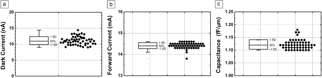
In CMOS integrated circuit (IC) foundries, the use of pure germanium for fabrication is considered “new,” thereby requiring careful introduction into existing manufacturing lines in order to minimize any undesirable impact on the momentum of ongoing production lots. For this effort, we successfully introduced Ge-integration with the existing Si-process line, while preserving consistent performance and yield. High-speed Ge photodetectors (>20 GHz) with low dark current (∼11 nA) and high responsivity (∼1.06 A/W) at 1550 nm were verified. Tight distributions in electrical device characteristics were achieved, as illustrated in Figure 8, indicating excellent process-control uniformity in the CMOS foundry.
Statistical plots for (a) dark current, (b) forward current, and (c) normalized capacitance (at |1V|) for an 8 × 25 μm2 Ge photodetector showing excellent uniformity.27 (SD = standard deviation)
Transfer evaluation results and (manufacturing) process readiness
Process modules were individually qualified during the technology transfer to ensure that the photonic device structures met the specifications in terms of dimension control and uniformity. For instance, for in-line process control, a post-etch final inspection critical dimension of 247.9 +/– 4.93 nm (mean +/– 1σ) with good process controllability, for example, a CP (process capability index CPK) of 2.03 (1.89) is typically obtained from a 0.18 µm CMOS wafer (for a 250 nm nominal critical dimension [CD] target). This again gives an indication of the strict process controls achievable from the manufacturing facility.
From wafer-level optical measurements, low-loss passives (e.g., waveguides [CD ∼500 nm] and bends [with a radius of 5 μm and a CD of ∼500 nm]) were achieved. The Si-channel waveguide loss was ∼1.8 +/– 0.2 dB/cm, Si-rib waveguide loss was ∼1.0 +/–0.2 dB/cm, and Si-bending loss was ∼0.014 +/–0.002 dB. These results were also verified at the die-level through edge-coupling from a lensed fiber and a 180 nm nano-taper with typical coupling loss <3 dB/facet.
In addition, MZI p–n junction-based Si modulators, a TiN heater for thermal-optics, and various efficient fiber-to-waveguide coupling schemes have also been established. Figure 9 shows an example of the MZI modulator, in which 4 mm Si MZI modulators exhibited typical figure-of-merit, the modulator efficiency, V πL of ∼2.3 V.cm (V π = applied voltage and L = device length for a 180° phase change) with phase shift insertion loss and device capacitance of 0.9 dB/mm and <0.4 pF/mm at –1 V, respectively. The loss and speed performance can be optimized via doping engineering, allowing further improvement of V πL for lower power operation and also higher speed,Reference Tu, Liow, Song, Luo, Fang, Yu and Lo30 in which an excellent 50 Gb/s modulating performance was obtained.
Efficient silicon Mach-Zhender interferometer modulator with low insertion loss and capacitance. (a) The spatial variation in the junction capacitance controlling the phase modulation is remarkably uniform; (b) the signal extinction dependence on wavelength and applied junction bias shows the behavior expected for an ideal Mach-Zhender interferometer; and (c) the optical phase shift is linear with applied bias voltage (V) for V < 6V with high efficiency indicated by a low V πL. Note: FSR, free spectral range; V π and L, applied voltage and device length for 180 degree phase change (maximum signal extinction), respectively.Reference Tu, Liow, Song, Luo, Fang, Yu and Lo30
Both lateral and surface couplings of light are facilitated by edge couplers and gratings, respectively, in this platform. For lateral coupling, a ∼120 µm deep Si trench with a smooth oxide sidewall facet (above the Si trench) eliminates the need for sidewall polishing. A suspended oxide coupler with a broadband wavelength operating range (>100 nm) and large fiber-to-chip alignment tolerance have been fabricated on the same platform. In summary, this enablement of an accessible commercial foundry caters to the increasing demands in silicon photonics prototyping and mass production needs.
Si-photonics and electronics integration platform/2.5D TSI
To date, silicon photonics technology has advanced and matured considerably with regard to the development of fundamental devices and establishment of commercialization pathways. With this, the next vital milestone is the convergence of electronics and photonics. In addition to the approach through monolithic integration,Reference Sahni, Ayazi, Chi, Dahl, De Dobbelaere, Gloeckner, Hon, Hovey, Liang, Mack, Masini, Mekis, Peterson, Pinguet, Schramm, Sharp, Sun, Timpe and Verslegers31,Reference Solomon, Shank, Green, Khater, Kiewra, Reinholm, Kamlapurkar, Rylyakov, Schow, Horst, Pan, Topuria, Rice, Gill, Rosenberg, Barwicz, Yang, Proesel, Hofrichter, Offrein, Gu, Haensch, Ellis-Monaghan and Vlasov32 heterogeneous electronic-photonic integrated circuits integration presents a more versatile alternative. It provides a path that harnesses the best performing electronics and photonics circuits, since each circuit type can be optimized using its own technologies and material systems without having to sacrifice their respective performance for the large-chip area difference, process thermal-budget incompatibility, and difficulty in managing large surface topographic features. 2.5D through-silicon interposer (TSI) is a technology platform that offers versatile heterogeneous integration capabilities for expanding the scope of applications with the mission of increasing functionalities (e.g., logic, memory, analog/mix-signal, radio frequency, microelectromechanical systems) and performance (e.g., shorter distance and finer bumping/solder features). In this platform, a chip area is allocated to host multiple functional guest chips (e.g., electronic or photonic integrated circuit, memories). This allocated chip provides the needed electrical metallization layers to connect all guest chips laterally and also to connect vias through silicon vertically to the bottom print-circuit-board. While the benefits of 2.5D TSI architecture have been actively explored in the last few years for memory and logics integration for attaining higher performance and lower power,Reference Solomon, Shank, Green, Khater, Kiewra, Reinholm, Kamlapurkar, Rylyakov, Schow, Horst, Pan, Topuria, Rice, Gill, Rosenberg, Barwicz, Yang, Proesel, Hofrichter, Offrein, Gu, Haensch, Ellis-Monaghan and Vlasov32,Reference Xie33 the integration of photonic functions is a critical strategy to meet many important performance targets needed for handling large data, lower power budget, and cost.
Figure 10 illustrates one of the implementation schemes. It has memory and logic on one side and optical I/O (input/output) on the other, complete with electrical connection via the bottom Si-interposer with both redistribution layers (RDLs) and through-silicon-vias (TSV). The driver and amplifier chips are flip-chip bonded on to a silicon photonic chip, which also has TSV connecting the electrical signals to the common (i.e., bottom) interposer for communicating with the memory/logic units. Thus, different from the monolithic approach, 2.5D TSI/3D IC technology is considered to be a more practical and versatile approach to integrate with silicon photonics. The TSI serves as a host to connect various functional chips and allows the photonics chips to be brought much closer to logic and memory chips, enabling higher I/O count scalability (e.g., with fine RDL pitch <2 μm and fine micro-bump pitch in the range of 10–40 μm) for higher data bandwidth and lower energy consumption (e.g., <pJ/bit) at lower cost.
Heterogeneous electronic and photonic integrated circuit integration based on the 2.5D through-silicon interposer (TSI) platform. This class of structures is the favored hybrid integration scheme preceding full monolithic integration. Note: TIA, transimpedance amplifier; TSV, through-silicon via; I/O, input/putput; PCB, print-circuit board; PD, photodetector; LA, limiting amplifier; MOD, modulator; MOD Drv, modulator driver; PIC, photonic integrated circuit; TSOI, through-silicon-optical-interposer.Reference Raghunathan, Ye, Hu, Izuhara, Michel and Kimerling7,34
Summary
As photonics has penetrated computation system design to shorter links, photonic components have become a larger fraction of the total system interconnection, and issues of system performance, manufacturing yield, and reliability are being reevaluated. Questions of chip design, redundancy strategy, assembly and packaging, modulation format, and the ability to support scaling of system density and input/output (I/O) bandwidth with low latency and energy have become fundamental. Data centers and high-performance computer installations today can feature as many as 20 million optical transceivers. Within the next five years, photonic interconnection for the PCIe processor to memory communication at the board level will be widespread. These high component counts far exceed current data communication and telecommunication demands. Silicon photonics is the unique platform that will deliver high volume manufacturing and cost reduction through monolithic integration. Silicon microphotonics today, as silicon microelectronics during the last 40 years, has the potential to satisfy these system constraints and provide 40 more years of performance scaling.
Acknowledgments
D.-L. Kwong would like to acknowledge funding from Exploit Technologies Pte Ltd (ETPL) A*STAR under “Silicon Photonics Commercialization Flagship Grant ETPL/11-R15FSH-001,” the collaborative efforts of GlobalFoundries Fab 3/5, Singapore, as well as P. Dong and Y.K. Chen from Bell Labs, Alcatel-Lucent in IME’s silicon photonics technology platform transfer, and M. Hochberg, T.B. Jones, and the team in the development of the optical wafer-level test set-up at IME.