I. INTRODUCTION
The past decade has witnessed a rapid growth in research on semiconductor nanowires that includes investigations of novel growth mechanisms and the exploration of size-dependent properties that can be exploited in a range of applications.Reference Schmidt, Wittemann, Senz and Gösele1, Reference Xia, Yang, Sun, Wu, Mayers, Gates, Yin, Kim and Yan2 The versatility of the vapor–liquid–solid (VLS) growth process,Reference Wagner and Ellis3 in which a liquid eutectic droplet promotes the crystallization of a single crystal nanowire, has supported the rapid expansion of nanowire research. Many other mechanisms can promote one-dimensional growth, however, including a vapor–solid–solid (VSS) process in which the seed particle is in the solid phase during growth.Reference Persson, Larsson, Stenstrom, Ohlsson, Samuelson and Wallenberg4 VSS growth can provide advantages over VLS growth,Reference Lensch-Falk, Hemesath, Perea and Lauhon5 including improved heterostructure junction abruptness,Reference Wen, Reuter, Bruley, Tersoff, Kodambaka, Stach and Ross6 reduced growth temperatures,Reference Arbiol, Kalache, Cabarrocas, Morante and Morral7–Reference Kang, Kim, Lee, Kim, Yang and Jo10 more narrow diameter distributions,Reference Lensch-Falk, Hemesath, Lopez and Lauhon11 better control of growth orientation,Reference Kang, Kim, Lee, Kim, Yang and Jo10 and increased purity as a result of the general reduction of impurity solubilities at lower growth temperatures.
In VSS as in VLS growth, the seed particle establishes an interface of preferred nucleation,Reference Wacaser, Dick, Johansson, Borgstrom, Deppert and Samuelson12 but there are important differences that may have consequences for the structure and composition of the product. Diffusion of atomic species to the growth interface may not occur through the catalyst particle,Reference Lensch-Falk, Hemesath, Perea and Lauhon5 which can alter the growth kinetics, and altered surface energies may influence phase, defect structure,Reference Arbiol, Morral, Estrade, Peiro, Kalache, Cabarrocas and Morante13 and growth direction.Reference Wu, Cui, Huynh, Barrelet, Bell and Lieber14, Reference Schmidt, Senz and Gösele15 In many earlier reports on VSS growth of Si and Ge nanowires, the metal catalysts are silicide and germanide phases.Reference Lensch-Falk, Hemesath, Perea and Lauhon5 In some interesting cases, the silicide and germanide phases themselves may grow in one-dimensional form.Reference Lensch-Falk, Hemesath and Lauhon16, Reference Schmitt, Higgins, Szczech and Jin17
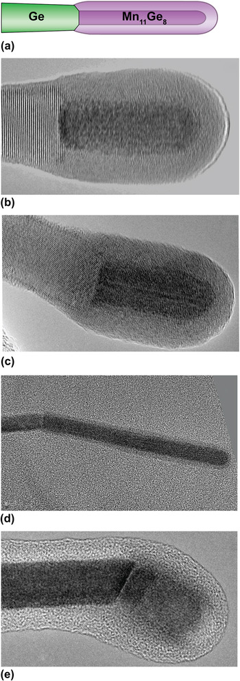
The joint growth of two phases from the same interface—syntaxial growth—was recently observed in Mn11Ge8-Ge nanowires (Fig. 1).Reference Lensch-Falk, Hemesath and Lauhon16 Syntaxially grown semiconductor–metal nanowire heterostructures are attractive because they provide a means to produce clean metal contacts during the growth itself. In addition, syntaxial growth provides interesting contrasts with VLS growth. In VLS growth, the nanowire is faceted but the liquid is not, and so they share no particular crystallographic relationship. The growth direction of nanowires above a critical size is established primarily by the energy of the liquid–solid interface.Reference Wu, Cui, Huynh, Barrelet, Bell and Lieber14, Reference Schmidt, Senz and Gösele15 In syntaxial VSS growth, which is also a near-equilibrium process, one expects to find relationships between the orientation of the metal catalyst and that of the semiconductor nanowire that minimize the energy of the configuration. The orientation relationships between Mn11Ge8 and Ge nanowire crystals are the subject of this study.
(a) Schematic of Mn11Ge8/Ge nanowire heterostructure. (b)–(e) Heterostructures with distinct orientations. Scale bars are 20 nm. (b) Germanide that grew parallel to the Ge growth axis. Germanides with other orientations were also observed: (c) 10°, (d) 20°, and (e) 35°.

In a polycrystalline material, the distribution of crystal orientations is referred to as texture.Reference Kocks, Tome and Wenk18 Texture may be of interest when crystalline anisotropies in intrinsic material properties lead to texture-dependent properties of a polycrystalline sample. Texture analysis has not previously been applied to a nanowire system, as these crystals are not polycrystalline in the conventional sense. For VSS growth, however, we may consider the crystalline seed particle the “substrate” and the distribution of nanowire orientations the polycrystalline “grains” that grow under the influence of the substrate/film interfacial energy. In this context, we have determined that Ge nanowires show a fiber texture with respect to the manganese germanide seeds; germanide nanowires grow only along the [001] direction, while Ge nanowires grow along [110], [111], and [112] crystallographic directions, as has been observed in VLS growth for Ge nanowires of similar diameters.Reference Wu, Cui, Huynh, Barrelet, Bell and Lieber14, Reference Schmidt, Senz and Gösele15 Furthermore, for the range of nanowire diameters produced from the growth process described here, the distribution of Ge growth directions is similar to what is observed in VLS growth, suggesting the energetics that dictate the resulting crystal structure and orientation for the two processes are similar. Generally, the Mn11Ge8/Ge nanowires do not exhibit biaxial texture, i.e., there is no preferred orientation of the two crystals across the shared interface. As VSS growth techniques have become more prevalent, it is important to identify the texture relationships that exist between catalyst particles and nanowires as the texture may influence important material properties, such as conductivity across the metal/semiconductor interface.Reference Kocks, Tome and Wenk18, Reference Randle and Engler19 Furthermore, the allowed crystallographic relationships ultimately delimit key outcomes of synthesis, including the growth direction and crystal phase.
II. EXPERIMENTAL
Mn11Ge8/Ge nanowire heterostructures were synthesized via chemical vapor deposition in hot-walled tube furnace. Mn seeds were formed on silicon nitride substrates by flowing H2 through a bubbler containing tricarbonyl (methylcyclopentadienyl) manganese (TCMn). Following Mn deposition, nanowire growth was initiated by co-flowing germane (10% GeH4 in H2) and TCMn. The seed formation and nanowire synthesis were carried out at a temperature of 350 °C, producing growth rate of ∼50 nm/min for the Ge nanowires and ∼5 nm/min for the germanide nanowires.Reference Lensch-Falk, Hemesath and Lauhon16 Transmission electron microscopy (TEM) imaging and electron diffraction were used for structural characterization. Nanowires were sonicated in ethanol and pipetted onto TEM support grids. Both silicon nitride membrane windows and lacey carbon supports on a Cu grid mesh were used for TEM characterization. High resolution TEM imaging and diffraction were performed on a JEOL 2100F.
III. RESULTS AND DISCUSSION
TEM imaging of many Mn11Ge8/Ge nanowire heterostructures indicated that the growth axes of the Ge and germanide were not always parallel, as shown in Fig. 1. Of the 91 nanowire heterostructures imaged in total, 64 (∼70%) exhibited a parallel alignment of growth axes, whereas the remaining 27 (∼30%) were not collinear, appearing as kinked heterostructures. In noncollinear structures, the growth axis of the germanide nanowire was perpendicular to the plane of the growth interface, whereas the growth axis of the Ge nanowire was not, as highlighted most notably in Fig. 1(e). The germanide nanowires terminated on c-planes, whereas the Ge nanowires terminated on (111), (110), or (112) planes. As shown below, Fig. 1 establishes the predominance of fiber and off-normal fiber texture in this system.
Texture analysis was used to determine whether the kinked heterostructures exhibit preferred orientations and, if so, to what degree. While macrotexture in populations of grains over large areas can be probed using either x-ray or neutron diffraction, individual grain orientations are often probed using scanning or TEM in a process commonly referred to as microtexture analysis.Reference Randle and Engler19 Classes of texture include (i) random texture, in which there is no preferred orientation; (ii) fiber texture, in which a crystallographic axis of the film is parallel with the substrate normal; and (iii) epitaxial or biaxial texture, in which alignment of the two in-plane axes fixes the crystallographic orientation of the film with respect to the substrate.
Though nanowire structures are not usually characterized in terms of texture analysis, the term becomes meaningful in the context of VSS growth, for which both the catalyst and the adjacent nanowire are crystalline during growth. Because the formation of metal nanoparticles precedes nanowire growth,Reference Cheng, Poon, Kok and Chan20–Reference Park, Kapur, Saraswat and Peng22 we consider each seed as the “substrate” with an exposed c-plane. The Ge nanowire crystal plays the role of the film growing from the seed substrate. As in a polycrystalline thin film, we expect that the presence of preferential orientations will reflect the relative magnitudes of interfacial energies, particularly the growth interface and the nanowire surfaces. High-resolution TEM (HRTEM) and selected-area electron diffraction (SAED) are the most appropriate methods to probe the texture of the nanowire heterostructures at this length scale; electron back-scatter diffraction can be applied to analyze crystals that are above ∼20 nm in size. The observed texture relationships can provide insight into the relative magnitude of the relevant surface energies, and such information is typically very difficult to obtain for nanostructures of this size regime. Texture analysis was applied to the examples presented in Figs. 2–4.
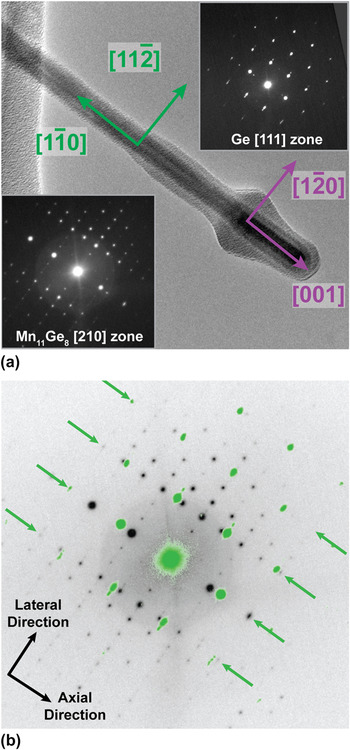
(a) TEM image of an epitaxial heterostructure. The irregular border is a result of carbon contamination from imaging. Diffraction patterns from the two crystals are given in the inset. In (b), the Ge diffraction pattern (green spots) is overlaid on that of the Mn11Ge8 to demonstrate the registry between planes (green arrows) perpendicular to the growth interface. Scale bars are 50 nm and 5 nm−1 for (a) and (b), respectively.

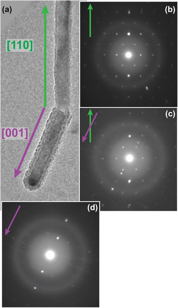
(a) TEM image of the region near the interface between Ge and Mn11Ge8 nanowires. Diffraction pattern of (b) the Ge nanowire only, (c) both crystals combined, and the (d) leader only. The Ge nanowire grows along a <110> direction, whereas the leader is oriented along a <001> direction, which corresponds to a <112> direction in the Ge. Green (purple) arrows indicate the growth axis of the Ge (Mn11Ge8) in both the image and the diffraction patterns. Scale bars are 25 nm and 10 nm−1 for (a) and (b)-(d), respectively.

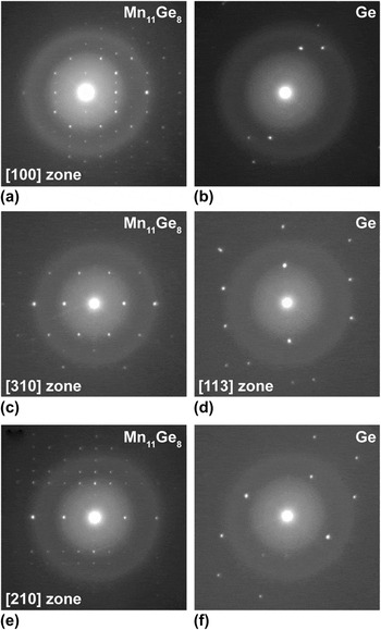
(a) Diffraction patterns from a single Mn11Ge8/Ge heterostructure with leader data (a, c, e) on the left and wire patterns (b, d, f) on the right. The data was collected as the leader was rotated about its axis to three different zone axis orientations. The {002} planes (perpendicular to the growth axis) are along the horizontal axis for all images.

A. Epitaxial texture
In one case, we observed the alignment of multiple distinct planes across the growth interface (heteroepitaxy). In Fig. 2, the growth axes of the germanide and Ge nanowires are parallel, and both are on low-index zone axes as indicated in the inset of diffraction patterns. This relative orientation aligns low-index lateral and axial directions in each crystal. As indicated by the arrows in Fig. 2(a), one can deduce that  along the growth direction,
 along the lateral direction, and parallel zone axes of [111]Ge and
 The heterostructure presented in Fig. 2 provided the only example of epitaxial texture for the 31 heterostructures in which the germanide orientation was obtained. The driving force for this type of texture is generally a low interfacial energy between a plane of the film and the surface plane of the substrate.Reference Randle and Engler19
This example of epitaxial texture enables us to highlight a feature of the interface that is likely present at all growth interfaces and which may be a key feature to enable this syntaxial VSS growth process. The overlaid diffraction patterns of the Ge and germanide [Fig. 2(b)] show that the (112) planes of Ge (2.305 Å) have a relatively low 1.6% mismatch with the (360) planes of Mn11Ge8 (2.269 Å). Despite the low lattice mismatch between these particular planes at the interface, there are additional lateral diffraction spots associated with the germanide that do not correspond to Ge spots. This is a natural consequence of the germanide unit cell being much larger than Ge. We expect, therefore, the presence of additional planes of atoms that terminate at the heterojunction, producing dislocations at this semi-coherent interface. While dislocations are undesired in some circumstances, it is possible that they are beneficial or even necessary in this context. It has been shown that diffusion of atomic species can increase by three orders of magnitude along dislocation cores in a process known as “pipe diffusion.”Reference Legros, Dehm, Arzt and Balk23 Given the fact that the germanide seed is a solid particle, this enhancement in the diffusion at the growth interface may play an important role in supplying adatoms to the crystallization interface during growth.
B. Fiber texture
In most cases, including kinked heterostructures, the growth interface corresponded to low-index planes for each phase. The lattice image of Fig. 1(b) resolves (002) germanide planes and (111) germanium planes that are parallel to one another and perpendicular to the common growth direction. The plane normals are collinear in both crystals, satisfying the requirement for fiber texture, which is the dominant class of texture for this system. It should be noted that if all reciprocal space could be probed, some examples of fiber texture may indicate additional crystallographic relationships and possibly an epitaxial texture. However, given the limited range of reciprocal space that can be probed in the TEM, it can be concluded that the samples demonstrate a fiber texture at a minimum.
Interestingly, for “kinked” structures, the angles between the germanide c-axis and the Ge nanowire growth direction consistently corresponded to angles between low-index directions in the diamond cubic crystal structure. For example, in Fig. 3, the Ge nanowire is growing along a <110> direction, and the germanide nanowire is oriented along the c-axis at a 30° angle from the axis of the wire. As indicated in the diffraction patterns in Figs. 3(b)–3(d), this kink corresponds to the angle between <110> and <112> directions in the diamond cubic lattice. This is the evidence that despite having a growth direction along the <110>, the Ge terminating plane at the growth interface is a {112} plane. In fact, the germanide nanowire axis is aligned with a low index direction in the Ge nanowire, for examples in Figs. 1(c)–1(e) and 3, which corresponds to an off-normal fiber texture.
C. Uniaxial in-plane texture
A shared feature of the epitaxial and fiber textures described earlier is that the growth axis of the germanide is collinear with a low-index crystallographic direction of the Ge nanowire. The diffraction patterns in Fig. 4 were taken on the only specimen for which the germanide growth axis did not appear to be aligned with respect to the Ge nanowire. In this case, the diffraction pattern of the germanide crystal was recorded first on the [100] zone axis and then on two higher-order zones; the [310] and the [210] axes were aligned through rotations of 21.8° and 31.0°, respectively, about the leader axis. The diffraction spots from {002} planes that are present in each pattern confirm that rotation occurred about the germanide growth axis. Despite the identification of three zone axes of the Mn11Ge8, the [113] zone was the only discernable orientation obtained for the Ge crystal.
Distinctly, the axis of the leader does not intersect the Ge reflections in any of the nanowire diffraction patterns of Fig. 4. This suggests that there is no axial crystallographic relationship between the two crystals, which is inconsistent with fiber and epitaxial textures. When the germanide is on the [310] zone axis [Fig. 4(c)], the nanowire is oriented to the [113] zone, which establishes that there is at least a uniaxial in-plane alignment at the growth interface where these two crystallographic directions are parallel. Given the limited range of reciprocal space that can be sampled using electron diffraction in the TEM, one cannot conclude that the texture is limited to only one single axis in the plane of the growth interface, but the data do indicate a rather weak crystallographic relationship between these two crystals.
Overall, fiber texture predominated for the Mn11Ge8/Ge heterostructures analyzed. The germanide was always elongated in the c-direction independent of the microtexture. Furthermore, we observed no correlation between kinked junctions and the growth direction or terminating plane of the Ge nanowire; examples of all three growth axes and terminating planes were found in both co-linear and kinked structures. Implications of this observation are discussed further.
Here, the Ge nanowire was considered as the “film” in the context of microtexture analysis, but there are important differences. First, the growth “direction” of a thin film is normal to the surface, whereas the nanowire growth direction may not be “normal” to its interface with a solid catalyst. The texture associated with highly anisotropic grains within a thin film would be more analogous to the nanowire texture described here. A second key difference between nanowire and thin film growth is the formation of stable surface facets present at the nanowire boundary. It has been proposed that nanowire growth directions arise as a result of the minimization of interfacial energy of the growth interface and these nanowire facets.Reference Wu, Cui, Huynh, Barrelet, Bell and Lieber14 Because the same growth directions were observed here for VSS syntaxial growth and previously for Au-catalyzed VLS growth, the relative influence of the Ge/Mn11Ge8 interfacial energy is comparable to that of the Ge/AuGe(l) catalyst. However, the magnitude of the interfacial energy varies with catalyst phase, and it can be sufficient to produce preferred growth directions and catalyst–nanowire orientations in VSS systems using alternative catalysts. As an example, Ge nanowires grown with a Cu3Ge catalyst exhibited exclusively <110> orientations.Reference Kang, Kim, Lee, Kim, Yang and Jo10 This highlights the potential to achieve control of nanowire orientation using an appropriately chosen catalyst phase.
IV. CONCLUSIONS
In summary, we have used TEM imaging and SAED to establish preferred growth directions and crystallographic relationships in the Mn11Ge8/Ge nanowire system. While the distribution of relative orientations in these heterostructures is not necessarily equivalent to texture relationships in polycrystalline thin films, the concept of microtexture is nonetheless useful in this context. The Mn11Ge8/Ge system generally exhibits a minimum fiber or off-normal fiber texture. For other systems grown by a crystalline catalyst in a VSS process, it is likely that texture relationships are present and can be established using the approach shown here. Texture relationships can influence the properties of heterojunctions involving anisotropic materials and can also provide insights into the influence of surface energies on the constituent phases and orientations in the resulting heterostructures.
ACKNOWLEDGMENTS
This work was supported by the National Science Foundation (E.R.H. and J.L.L.). We thank Dr. Jinsong Wu for assistance in the interpretation of diffraction data. Electron microscopy measurements were conducted in the EPIC facility within NUANCE center at Northwestern University.