Introduction
In the contemporary world, a requirement of low profile and radiation efficient antennas are in demand for high-speed wireless, satellite, radar and aircraft applications. Microstrip slot antenna finds its numerous applications due to its low-cost design, small size, low weight, and suitable isolation from feeding network and easy integration with planar circuits [Reference Yoshimura1]. Few researchers have proposed slot antennas using microstrip technology. In [Reference Elazar and Kisliuk2] the author has developed the thirteen element linear slot antenna array for the X band and forms the relation to compute the mutual coupling between the slots and E/H plane field. The major drawback of the slot antenna is a bidirectional radiation pattern. To reduce the back radiation, a metal reflector or a shallow cavity can be introduced [Reference Luo, Hu, Dong and Sun3,Reference Adams4]. The use of a non-planar cavity at the back of the slot is bulky and consumes a large area [Reference Mukherjee, Biswas and Srivastava5].
Substrate integrated waveguide (SIW) is a promising technology to transform the non-planar conventional waveguide structure into a planar form [Reference Bozzi, Georgiadis and Wu6]. The foundation of SIW was previously laid by D. Deslandes; K. Wu in [Reference Deslandes and Wu7]. SIW is made up of metallic via side walls separated by a distance “p” and sandwiched between the two metallic plates on each side of the substrate. The SIW technology can be used to form the cavity [Reference Cassivi, Perregrini, Wu and Conciauro8], which can be formed by enclosing all sides by the four rows of metallic vias. The application of the SIW cavity was further extended to form an antenna in [Reference Luo, Hu, Dong and Sun3]. This technology replaces the non-planar form of the metallic cavity to reduce the back side lobe and provide a directional radiation pattern [Reference Mukherjee, Biswas and Srivastava5].
In the present endeavor, a 1 × 6 slot antenna array is proposed which is enclosed inside a SIW cavity. As the SIW cavity gives advantages over conventional methods of making a non-planar cavity, the proposed antenna has the advantage of reduced back lobe radiation. Due to the reduction in the back lobe, the proposed design gives high gain, improved radiation efficiency by giving an advantage of low cost and compact size. The two L-slots presents inside the sub cavity, try to minimize the electrical length in comparison to straight rectangular slots, hence reduces the size of an antenna. The slots are created by putting two L slots inducted one above the other. The edges of the L slots are curved to improve the gain. Due to the curve structure at the edges, the losses occurred due to corners reduced considerably to achieve significant gain improvement. On a ground surface, two defective ground structure (DGS) are introduced to improve the flow of current to the terminal slots. The DGS was created by two split rings slots at both ends. The antenna is fed by a through-hole SSMA connector.
When compared to the available literature, the proposed design has high gain and small size with respect to the number of slots and the frequency of operation. The available literature either cited high gain due to higher frequency of operation or due to the introduction of a number of elements.
The slot separated by one-half the guide wavelength to form an array achieves a high gain and directive pattern [Reference Yan, Hong, Hua, Chen, Wu and Cui9]. The study of L-slot antenna is done by the authors in [Reference Srivastava, Chaudhary, Biswas and Akhtar10], where an L-slot is made by combining longitudinal and transversal slot antenna. Several literature studies are available which prove that the array formation of slot antenna can provide high gain. In [Reference Wen, Wang and Ding11] four inclined slots are created in a SIW cavity and further multiplied to form 1 × 8 a phased array antenna. The 45° inclined slots are created in a series and enclosed in a SIW cavity was done by the authors in [Reference Kim, Chung, Park, Lee and Nam12]; where the antenna works for Ka-band frequency. In [Reference Yang, Zhao, Yang, Liu and Liu13] single layer monopulse antenna was proposed which was fed from two different ports. The antenna was formed by two subarray of slots placed in cavity-2 and cavity-3. A single layer, dual-frequency slot antenna was proposed by the authors in [Reference Yang, Cao and Pan14]. The antenna has two ports; each of it is used to resonate the antenna at different frequencies. The prototype has 24 elements to achieve high gain. A wideband slot antenna array was proposed by [Reference Herrero-Sebastián and Benavente-Peces15], where the reflection-slope method was introduced to optimize the position of the slot. The working of the antenna was optimized to sub-6 GHz band for 5 G applications. A 4 × 4 planar slot antenna was proposed by the authors in [Reference Yang, Zhao, Yang and Nie16], where the antenna is fed by a feeding network from the bottom of the SIW cavity. But all of the designs either are working at a higher frequency band or has a larger number of slots enclosed in a SIW to achieve high gain.
The proposed antenna is fabricated on 3.18 mm RT/Duroid 5870 substrate with ɛ r = 2.33. The design was simulated and verified using the High-Frequency Simulation Software. The antenna was optimized on various parameters to achieve a high gain at 14.29 GHz.
Antenna geometry
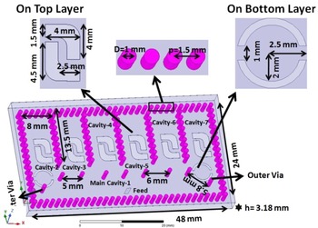
The SIW cavity of size 3.6λ g × 1.8λ g is used to enclose six L-slot antenna pairs. The antenna elements were further separated from each other by the via boundary to form sub-cavities of size 1.0λ g × 0.6λ g as shown in Fig. 1.
The proposed antenna design.

The dual L-slots are clubbed together in inverted form to produce inductive and capacitive loading. The direction of the wave along the y-axis is affected by the parallel combination of an inductor (due to slot) and capacitor (due to the gap between two slots). The corners of the L-slots are curved to improve the gain by almost 0.3 dB. The overall structure is divided into seven different cavities. Cavity-1 is used to feed the L-slots available in the remaining six sub cavities. The main Cavity-1 is having a metallic vias in-front of the sub-cavities, which was introduced to help individually feed the slots in cavities. The positions of these vias are optimized to improve the front to back and side lobe radiation ratio and hence achieve the desired gain. The design is fed by a lumped port, the position of which is adjusted after a detailed parametric study. The L-slots are created on the top copper layer of the substrate, while DGS is created at the bottom surface. The position and the inner /outer radius of the DGS are also optimized to achieve a low side lobe level. The design also integrates two metallic vias just below the DGS structure. These vias help to modulate the current till the last L-shaped slots. Various parameters of the design are given in Table 1.
Design parameters

Working principle
The resonant frequency of the sub-cavity containing the L-slots can be calculated by using equation-1[Reference Cassivi, Perregrini, Wu and Conciauro8].

where,

and

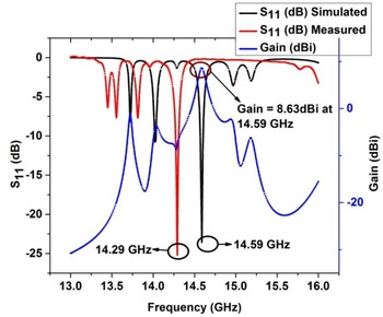
‘D” is the diameter of the via, whereas “p” is the pitch of the via. The above equations are only valid for $b < \lambda _o.\sqrt {\varepsilon _r} /2$ and b < 4D. The above formula got verified for sub-cavity, by putting the value of “D” = 1 mm, “p” = 1.5 mm, “L” = 13.5 mm, “W” = 8 mm, “ɛ r” = 2.33 and the height of the substrate “h” = 3.18 mm. The cavity resonates at 15.5 GHz in its fundamental TE101 mode. The resonant frequency in the measured result is 14.29 GHz whereas in the simulation it is 14.59 GHz. This proves the closest approximation of the resonant frequency in theoretical, simulated and measured results. The resonant frequency shifted to the left due to the inductive loading of the slots created inside the cavity. This also helps to miniaturize the antenna for the given frequency of operation.
The array factor of the proposed 1 × 6 antenna array can be evaluated by using equation (4) and (5) [Reference Balanis17].

where,

Here, β is the successive phase difference between the antenna elements, “d” = 8 mm/0.55λ o is the distance between the two antenna elements and “N = 6”, k is the free space wave number.
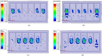
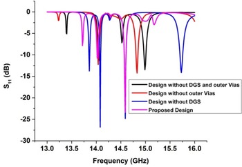
The advantage of using end metallic vias and DGS structure can be seen in Fig. 2. It is clear from Fig. 2(b) that the outer metallic vias helps to restrict the maximum current to flow on the outer L-slots. Figure 2(c) shows that the DGS structure allows some amount of power to flow to the outer L-slot, which in turn improve the overall gain of the antenna. The comparison of the designs shown in Fig. 2 is explained on the basis of S 11 (dB) parameter through Fig. 3.
The current distribution in structure at 14.59 GHz (a) without DGS and outer slots vias (b) without outer vias (d) without DGS (c) proposed design.

Comparison S 11 (dB) graph for various designs.

The S 11 (dB) comparison graph shows one important aspect of the design. The design without DGS shows one more prominent frequency of operation at 14.08 GHz, which was quite suppressed in the proposed antenna design with the introduction of DGS. The reason not to include the lower frequency is that the radiation pattern at 14.08 GHz for the design without DGS shows a dip in the center.
Simulated and measured results
The device is fabricated through a PCB prototyping machine on an RT/Duroid Roggers substrate of thickness 3.18 mm.
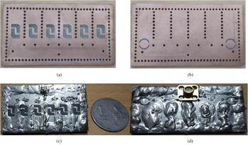
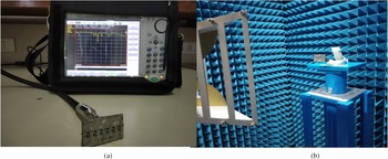
Due to the use of the thicker substrate, the process of creating the printed though hole across it was typical, hence the vias are filled with copper wire and soldered at both ends as shown in Fig. 4. During this process the copper layer on the top and bottom layers were tined. Tinning is a common phenomenon in PCB design and does not affect antenna parameters to a larger extent. The proposed design was tested for S 11 (dB) parameter on the Antrisu Site Master, S820E VNA for 30 GHz. The test bench of the antenna under test can be seen in Fig. 5(a). Figure 5(b) shows the Anechoic Chamber setup for testing antenna radiation pattern and gain.
The fabricated antenna prototype (a) Top layer (b) Bottom Layer (c) Top layer after tinning process (d) Bottom Layer after tinning.

Antenna under test at (a) Antrisu Site Master, S820E VNA (b) Anechoic Chamber for testing antenna radiation pattern and gain.

The S 11 (dB) of the proposed antenna is shown at Fig. 6. The measured results shifted left by 0.3 GHz. The shift can be explained by the loading done by tin material at the top and bottom layer of the antenna. The lower frequency band in the measured S 11 (dB) is suppressed by a considerable amount, so the band can be neglected. The measured result shows that the antenna achieves a 10 db bandwidth of 44 MHz.
Tested and Measured S 11 (dB) parameter with Gain (dBi).

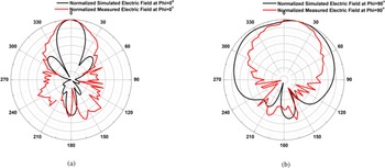
Figure 6 also shows that at the operating frequency of 14.59 GHz the antenna shows a gain of 8.63 dBi. The measured gain at 14.29 GHz is calculated as 8 dBi when the distance between the test antenna and referenced antenna is kept 1 m and the gain of the referenced double ridge horn antenna at 14.29 GHz is 14.35 dBi. Figures 7(a) and 7(b) shows the measured and simulated normalized electric field for two planes (a)angle phi = 0° (xz plane) and (b)angle phi = 90° (yz plane) for the proposed antenna.
Electric Field (a) measured and simulated for angle phi = 0o (b) measured and simulated for angle phi = 90o.

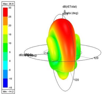
The two dimensional and three-dimensional electric field in Figs 7 and 8 respectively, shows that the radiation pattern is projected only in a single direction. A high directive beam with low side and back lobe radiation leads to achieving a high gain. The FBR of the proposed antenna structure is 24.9 dB.
Three-dimensional electric field.

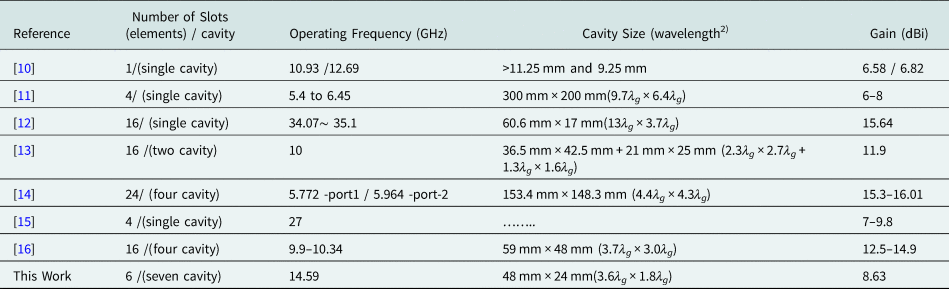
The comparison of the proposed design is done in Table 2, with seven different references cited in this communication. From Table 2 it is clear that the proposed antenna design is smaller in size and achieves good gain.
Comparison Table
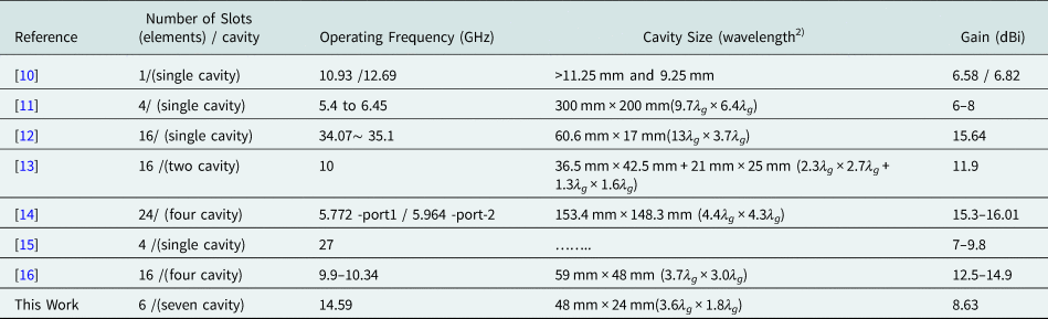
Since, there are limited numbers of designs of the L-slot antenna, hence the major comparison was done with other types of the slot antenna enclosed in a SIW cavity and further divided into sub cavity. In [Reference Wen, Wang and Ding11], the author further replicated his design to form a phased array antenna, hence the comparison was done only with a single element slot antenna.
Conclusion
This article proposed a novel dual L-slot array antenna structure with DGS on the ground plane, which achieves high gain and low front-to-back lobe ratio. The design of the antenna is simple which makes it easier to fabricate at a low cost. The antenna is compared with other designs based upon its operating frequency and gain (dBi). The simulated results show a narrow half-power beamwidth of 25 degrees, which can be used for various high-frequency applications working in the Ku band. The design can be replicated to form a bigger array, which can be used for the front end antenna in the satellite communication.
 Mr. Abhay Kumar is currently pursuing his PhD and serving as assistant professor in the Department of Electronics and Communication Engineering at Jaypee Institute of Information Technology, Noida, India. He received his M.Tech degree in Communication Engineering Department from IIIT Allahabad in the year 2014 and a B.Tech degree in the Department of Electronics and Communication Engineering from JSS Academy of Technical Education Noida in the year 2010. He received the Institute Gold medal for his M.Tech degree. He has 2 years of industry experience and 6 years of teaching experience. His area of interest includes substrate integrated waveguide (SIW), millimeter wave technology and microwave circuits. He is a member of IEEE.
 Dr. Shweta Srivastava received her B.Tech degree from IPST in 1998 and Ph.D degree from the Indian Institute of Technology, Banaras Hindu University, India in 2002. She joined Birla Institute of Technology, Mesra, Ranchi, India in February 2002 as a faculty member. She was awarded SERC fast track project for young Scientist by the Department of Science and Technology, Government of India. She joined Jaypee Institute of Information Technology, Noida, India in 2014 and is presently serving there as professor and Head of the Department of Electronics and Communication Engineering. Shweta Srivastava has published more than 80 research papers in peer-reviewed and reputed journals and conferences. She was awarded Smt. Ranjana Pal Memorial Award from IETE and the award for outstanding women in engineering by Venus foundation. Her areas of interest include microwave circuits and antennas, microstrip technology, SIWs, millimeter wave technology etc. She is a member of several professional bodies such as IEEE, ISTE, IETE etc.