I. INTRODUCTION
In the last decade, numerous wireless systems are noticed for some special benefits such as simplicity, low cost, and easy operation. Nowadays, wireless local area network (WLAN) systems are widely used because of appropriated price, high-speed data transfer. IEEE 802.11a, IEEE 802.11bg, and Hyper LAN/2 standards are covered WLAN frequencies. The IEEE 802.11 standard has three frequency bands at 2.4 GHz (2.484–2.4), 5.2 GHz (5.35–5.15), and 5.8 GHz (5.825–5.725) and the frequency range in 3.3–3.8 GHz, which has been allocated for wireless personal area network (WPAN) and WiMAX [Reference Boroomandisorkhabi, Sadeghzadeh, Zarrabi and Ghahramani1–Reference Choe and Lim3]. New modern communication systems need microwave components with high performance and small size, so compact antennas are required. Furthermore, microstrip antennas are used in aviation, space exploration, satellite, missile, and various governmental and commercial applications, because of suitable size, weight, price, performance, and ease of installation [Reference Rahimi, Zarrabi, Ahmadian, Mansouri and Keshtkar4]. Many researchers focus on achieving miniaturized, compact, multi-frequency, and power efficiency of the antennas. So many researches have been done on antenna miniaturization and various methods have been used for designing small antennas such as loaded antennas with lumped elements. The application of high dielectric constant materials [Reference Lee and Harackiewicz5], the application of slotted ground and short circuit [Reference Wang and Yang6], the optimal antenna geometry [Reference Xiao, Wang, Shao and Zhang7], the fractal antenna [Reference Borja and Romeu8], and using of the composite right/left-handed (CRLH)-TL technique [Reference Deng, Li, Xie and Yin9] are noticed for miniaturization. Electromagnetic band gap (EBG) structures are well-known metamaterial with a periodic structure that consists of metal or dielectric elements, which are showing the band pass or band stop characteristics [Reference Kim, Nguyen and Jang10]. Different form of planar EBG structures like a mushroom and fractal shape is provided in order to develop the bandwidth, phase characteristics, and coupling decreased characteristics. Some studies have been performed by modeling equivalent circuits [Reference Mohajer-Iravani and Ramahi11]. Fractional pattern is broken or irregular fragments and a family of complex shapes that has self-similarity or self-affinity in their geometrical structure. They are common shapes in the nature such as snowflakes, ferns, trees, coastlines, mountain ranges, and even galaxies. The self-similar geometries also could be useful in antenna engineering applications. Self-similar antennas are multi-resonant and small multi-band characteristics have been associated with the self-similarity of the geometry. Meanwhile, dimensions are associated with the size [Reference Zhang, Yin and Ma12]. Bow–Tie Dipole antenna with Koch shape fractal has been designed for multi-band and miniaturization [Reference Li and Mao13]. In addition, fractal-shape patch-slot configuration is used in miniaturized reflect array unit cell and Minkowski fractal is compared for different steps [Reference Oloumi, Ebadi, Kordzadeh, Semnani, Mousavi and Gong14, Reference Mahatthanajatuphat, Akkaraekthalin, Saleekaw and Krairiksh15].
Over the last decades, by the development of the satellite communication; the circular polarization (CP) antennas are used for communication links to reduce the natural loss effect in receivers. Global positioning system, the CP antenna is necessary. CP in antennas reduces the losses caused by multipath effects, between the transmitter and the receiver antennas. The CP antenna, with its low profile, small size, and lightweight, is ideal for portable wireless application. Therefore, the circular slot antenna with the TE11 mode with c-strip metal for CP is noticed [Reference Chen, Chiu, Lin and Yeh16]. Circularly slotted ground plane with a pair of spur-shaped slits and protruded arc-shaped metallic strip with a circular slot in coplanar waveguide (CPW) are introduced as a well-known method for CP application [Reference Ojaroudi, Ojaroudi and Ghadimi17, Reference Chiang, Hung and Bor18] and annular-ring slot antenna with a pair of slits and truncated corner is reported by Kumar et al. [Reference Kumar, Gautam and Kanaujia19].
The equivalent circuit is one of the best methods to describe the effect of each element in microstrip devices such as antennas, filters, and couplers. The gaps in the microstrip structure are modeled as capacitance. Meanwhile, for designing an inductance, the microstrip line and via are used [Reference Ha, Kwon, Lee and Choi20, Reference Park, Ryu, Lee and Lee21]. Therefore, the gaps are noticed as a capacitance in metamaterial structures such as EBG and split-ring resonator (SRR) that are used in this paper. In EBG, unit cells via are used for making inductance accordingly.
Controlling of mentioned capacitance and inductance in EBG and SRR would lead the antenna and frequency to be miniaturized and tuned.
In this paper, the combination of EBG and SRR loads with the fractal formation is noticed to miniaturize the microstrip antennas. Two-difference shapes of antennas are studied with two well-known metamaterial structures as a parasitic element. Here, designing steps of each antenna are presented. The antenna S-parameter is compared in designing step. Finally, a comparison between simulated antennas with experimental one is presented for S-parameter and radiation pattern. In the second antenna, we have shown that SRR load could be helpful for making the CP with a little change in the feed line. In design part, we modeled the antennas and then we described the result with numerical relation and the final equations can be used for redesigning of the antenna for difference frequency with selecting main patch or slot antenna and EBG cells. The simulation results are obtained with the three-dimensional (3D) electromagnetic simulator HFSS and compared with the experimental.
II. ANTENNA STRUCTURE
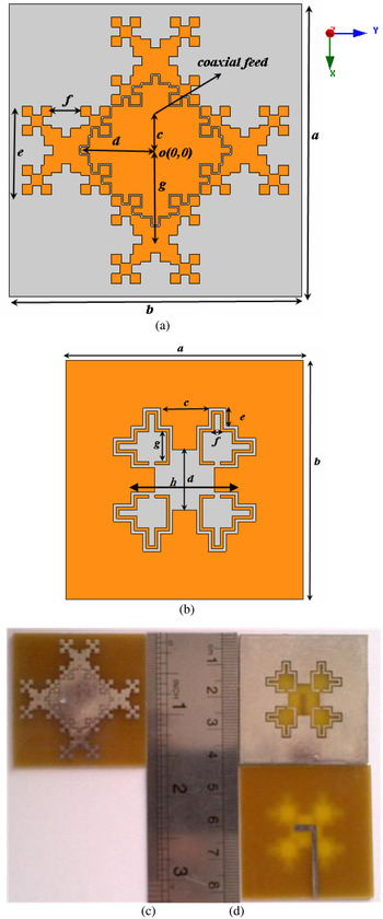
Figure 1 shows both proposed antennas configuration. The antennas are printed at a FR-4 low-cost and lossy substrate with relative permittivity of 4.4 and a thickness of 1.6 mm. The total size of each antenna is 40 × 40 mm2. As shown in Fig 1(a), the first antenna is a patch antenna with four EBG unit cells, which is used Minkowski fractal formation that is fed by coaxial feed line. The second antenna is a microstrip slot antenna with a width of 2 and 22 mm length of feed line that is connected to the 50 Ω SubMiniature version A (SMA), and it is fabricated on FR-4.
Prototype antennas (a) first antenna geometry, (b) second antenna geometry, (c) first antenna fabricated, and (d) second and third antennas fabricated.

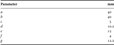
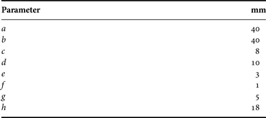
The fabricated antenna is shown in Figs 1(c) and 1(d). The antenna geometry details are presented in Table 1 for patch antenna with EBG unit cells and Table 2 shows the microstrip slot antenna with SRR load.
Geometrical parameters of the patch antenna with EBG.

Geometrical parameters of the slot antenna with SRR load.

A) Patch antenna with EBG unit cells simulation and measurement
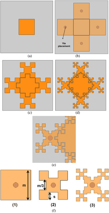
Figure 2 shows the four steps of designing a simple patch antenna and patch antenna with EBG unit cells where four EBG structures surround a simple microstrip patch with a 0.2 mm gap. The via's radius is 1 mm and EBG width is 12 mm and Fig. 2(b) is transparent to reveal via's connection. In Figs 2(c)–2(e), the patch antenna shows the Minkowski fractal structure, which is applied to patch and EBG unit cells. Figure 2(f) shows the steps of the Minkowski fractal design. The geometry of Minkowski is created using iteration factor as depicted by Mahatthanajatuphat et al. [Reference Mahatthanajatuphat, Akkaraekthalin, Saleekaw and Krairiksh15] and generally, the value of s is smaller than m/3.
Patch antenna with EBG unit cells (a) simple patch antenna, (b) first order of fractal formation, (c) second order of fractal formation, (d) third order of fractal formation, (e) final fractal unit cells, and (f) steps of designing Minkowski fractal.

Here EBG cells are used as a left-hand material with the specified capacitance and inductance. Edge capacity and inductance for a narrow slit are obtained by the following equations [Reference Yang and Rahmat-Samii22]:
 $$C = \displaystyle{{W\varepsilon _0 (1 + \varepsilon _r )} \over \pi} \cosh ^{ - 1} \left( {\displaystyle{{W + g} \over g}} \right),$$
 $$L = \mu h.$$
As show in (1), the gap is modeled capacitance and it is proportionate with the width of the EBG cells, which is showed by W. Therefore, when the fractal model is combined with this structure, the width of EBG unit cells is increased and higher capacitance for EBG cells would be expected.
The metamaterial CRLH cells are contained right-hand (RH) and left-hand (LH) parts.
In this structure, the patch makes RH frequency and EBG cell frequency is making LH frequency. As a result, in the the final model, frequency is obtained by (3):
 $$f_{ZOR} = \sqrt {f_{RH} \times f_{LH}}. $$
For modeling of the fractal ratio in each step is obtained by calculation of the width in each step for capacitance and for patch size we have divided each step to original patch.
Here for the second step, as shown in Fig. 2(b), the C and L are obtained 0.87 Pf and 2.01 nH, respectively, by (1) and (2). In this case, the LH frequency is 3.79 GHz by numerical modeling for gap capacitance and via inductance from (1) and (2) and by simulation of simple patch, we can assume RH frequency as 5.53 GHz. Therefore, the zeroth-order resonance (ZOR) is obtained 4.57 GHz and simulation is achieved at 4.59 GHz by (3).
In the third step, we have increased the effective capacitance length and the ratio of new length to pervious length is 1.47. Consequently, the LH frequency is around 2.57 GHz and by simulation of fractal patch, we can assume RH frequency of 4.55 GHz. Therefore, antenna resonance should reduce and we will have 3.41 and 3.02 GHz for numerical and simulation, respectively. The most mismatching between the numerical and simulation is appeared in this step, which is near 0.39 GHz.
In the final antenna, the effective length ratio is about 2.50. Then the LH frequency is about 1.51 GHz and for the RH most part, we have two resonances at 4.09 and 5.61 GHz. Therefore, antenna resonance should reduce to 2.48 GHz for numerical modeling where the resonance at simulation is occurred at 2.55 GHz. Therefore, we have less mismatching between simulations and numerical that is <0.07 GHz.
The patch antenna size ratio in the third and fourth steps is 1.3 and 1.48.
Apparently, the prototype antenna of first resonances can be assumed as a ZOR and it can be obtained by (4):
 $$f \approx \sqrt {\displaystyle{{f_{RH}} \over {2\pi \alpha \beta \sqrt {LC}}}} \;{\rm or}\;f \approx \displaystyle{{\sqrt {f_{RH} \times f_{LH}}} \over {\sqrt {\alpha \beta}}}, $$
where α and β are the capacitance ratio and patch size ratio, respectively. The f RH and f LH are known as right-and left-hand frequencies, respectively that are obtained from patch simulation and EBG unit cells calculation.
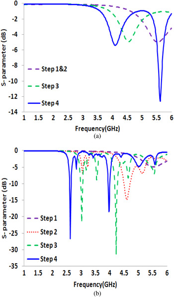
Figure 3(a) shows the S-parameters, which are used in the antenna patch without EBG unit cell and Fig. 3(b) shows the S-parameter beside an antenna patch with EBG.
Simulation for each step of design (a) fractal formation effect of patch resonances and (b) fractal formation and EBG unit cells effect on antenna resonances.

The simple patch antenna does not have effective resonance at a range of 1–6 GHz and it has weak resonance at 5.5 GHz. At the first model of fractal which is in a third step, the frequency resonance is reduced to 4.5 GHz and at the fourth step, the patch frequencies are occurring at 4 and 5.5 GHz as shown in Fig. 3(a) as a dual-band characteristic.
The antenna shows a good resonance at 4.5 GHz in the second step when EBG unit cells are added to the antenna.
The fractal structure antenna shows a dual-band characteristic with resonance at 3.01 and 4.25 GHz. In the fourth step, when second-order Minkowski fractal is implemented, the antenna shows a dual-band characteristic with resonance at 2.5 and 4 GHz.
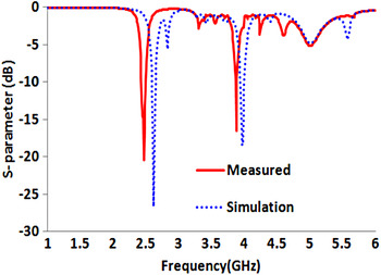
Figure 4 shows the comparison between S-parameter of the final model antenna simulation and experimental measurement and a good agreement is obtained between simulation and measurement results. For the experimental result, we are obtained two resonances at 2.46 and 3.88 GHz with 3.2 and 1% bandwidth, respectively.
S-parameter for measurement and simulation.

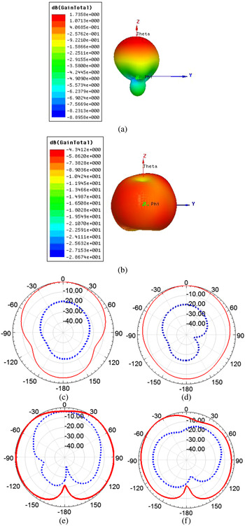
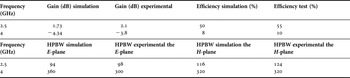
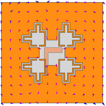
The maximum gain of the antenna at 2.5 GHz is about 1.73 dBi and the antenna has a directional pattern as shown in Fig. 5(a). For patch antenna, the directional pattern is expected and as shown in Figs 6(a) to 6(c), the current is concentrated at the patch and the inner side of the EBG cells and it can prove the pattern formation.
Antenna pattern for co- and cross-polarizations (a) 2.5 GHz, (b) 4 GHz, (c) E-plane measured at 2.5 GHz, (d) H-plane measured at 2.5 GHz, (e) E-plane measured at 4 GHz, and (f) H-plane measured at 4 GHz (solid line for co-polarization and dash line for cross-polarization).

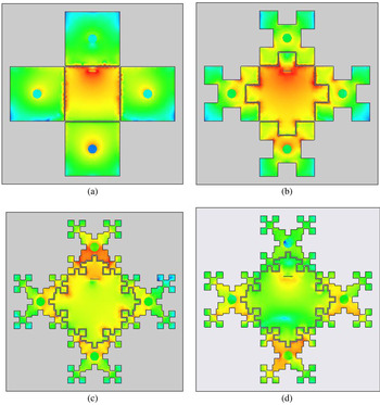
The first antenna current distribution at their (a) first steps of design at 4.5 GHz, (b) second step of design 3 GHz, (c) third step of design at 2.5 GHz, and (d) third step of design at 4 GHz.

However, the second resonance has an omni-directional pattern with a gain of −4.34 dBi at 4 GHz as shown in Fig. 5(b). Through the mentioned frequency, omni-directional patterns have been reached which can be justified with current distribution as shown in Fig. 6(d). The current is concentrated on the outer side of the EBG cells, which make the omni-directional pattern formation and we can justify non-uniformity of the H-plane pattern of current distribution as shown in Fig. 5(f).
Figures 6(a)–6(c) show the antenna current distribution of resonance frequency at 2.50 GHz and for second resonance at final antenna is presented in Fig. 6(d). As showed in Fig. 6(a), the current at the first step is not distributed completely in total surface and its concentrate in patch area and EBG cells has less current density. Figures 6(b) and 6(c) show the current distribution where fractal formation is implemented. In these conditions, the current is distributed more into the EBG fractal cells and fractal arrangement is helpful to reduce current density in the patch antenna. Meanwhile, with comparison among Figs 6(a) to 6(c) we could realize that the current distribution in the antenna surface is getting a uniform formation. Typically, in ZOR antennas, the current should distribute even in unit cells as shown in Fig. 6(c).
The measured radiation patterns in the E- and H-planes for 2.5 and 4 GHz are presented in Figs 5(c)–5(f).
The antenna pattern shows good similarity between simulated and experimental results and the antenna shows directional and omni-directional characteristics, respectively, at 2.5 and 4 GHz. Meanwhile, it can be seen that after the frequency increment, the CP level of the antenna in the E- and H-planes, is increased remarkably. Radiation parameters that are compared between the simulation and experimental results are presented in Table 3 for 2.5 and 4 GHz. The antenna gain between measurement and simulation are following each other. At the second frequency, the antenna gain is reduced drastically to −4.34 dBi and at this frequency, the antenna efficiency is reduced to 8% so the mentioned resonance has less effect in the communication system and it is a resonator, not an antenna resonance.
Radiation parameters for first antenna, simulation, and experimental results.

The antenna radiation gain and efficiency at the second resonance is lower than the first resonance and conventional antenna, but the first resonance has typical efficiency that is comparable with the other metamaterial antenna.
B) Slot antenna with SRR load
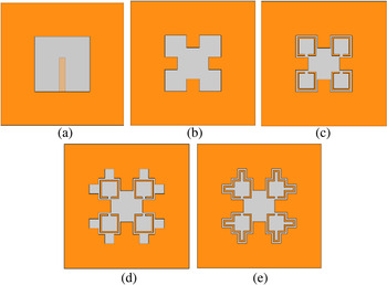
Figure 7 shows five steps of designing a slot antenna with SRR unit cells. At the first step, Fig. 7(a) shows a conventional slot antenna microstrip feed line. In the second step, a Minkowski slot is replaced with a simple slot as shown in Fig. 7(b) and the SRR load is added to the antenna (Fig. 7(c)), then in the fourth step as shown in Fig. 7(d), the second step of Minkowski applying for the slot part and at the end the fractal formation also applied to SRR structure as shown in Fig. 7(e).
Slot antenna with SRR unit cells (a) conventional slot antenna, (b) first step Minkowski slot, (c) first-order Minkowski slot with SRR, (d) second-order Minkowski slot with SRR, and (e) second-order Minkowski slot with developed SRR.

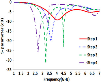
Figure 8 shows the variation in S-parameters for the second antenna for the steps first to fourth. The first antenna has one resonance at 4 GHz with S 11 around −8 dB with a Minkowski slot implementation that shows effective resonance at 3.5 GHz in the antenna. Therefore, the first order of a Minkowski helps to miniaturize it about 0.5 GHz. In the third step, the SRR implementation has helped the antenna to minimize to 3.1 GHz where another antenna resonance is occurred at 4.5 GHz. When the second-order Minkowski is applied to the antenna, then the resonance is reduced to 2.6 GHz.
Simulation of the second antenna from first to fourth steps.

So for a conventional slot (Fig. 7(a)) the resonance is obtained at 3.98 GHz and it is about 4 GHz for simulation. For the second step, the effective length (d) is increased to 24 mm and frequency is obtained 2.99 GHz where simulation is achieved 3.5 GHz and these resonance frequencies of slot can be obtained from [Reference Krishna and Kumar23].
In the third step, the SRR element is adding a capacitance and inductance to the antenna equivalent circuit, so we expect two resonances.
In the second step, we obtained the first resonance at 2.99 GHz and the second resonance can be achieved by assuming the length of SRR instead of (d). Therefore, for d = 16 mm we are obtained 4.48 GHz and for simulation, we have a dual-band structure at 3.1 and 4.5 GHz. In the fourth step, with changing the size of slot formation, the effective length (d) is increased to 28 mm and frequency is obtained 2.56 GHz where simulation is achieved 2.6 GHz. The new gap between ground and SRR is affected on SRR frequency, it is shifted to 6.5 GHz and the combination of two-resonance circuit caused another unexpected resonance at 3.5 GHz.
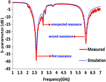
In the final model, the effective length of SRR is increased that caused to reduce the second resonance to 5.9 GHz, which have made an unexpected harmonic and become a part of the first resonance as shown in Fig. 9.
Return loss for measurement and simulation.

The final antenna return loss simulation and measurement are compared in Fig. 9. As shown in Fig. 9, the antenna has two resonances at 2.5 and 5.9 GHz for dual-band application at WLAN with 27.5 and 8% bandwidth, respectively, for the first and second resonances and a good agreement is visible between the simulation and measurement results. This kind of antenna has more gain and efficiency in comparison with patch antennas. The conventional gain of this structure is more than 3.5 dBi with more than 70% efficiency. While for the first resonance, the antenna efficiency is increased to 92%.
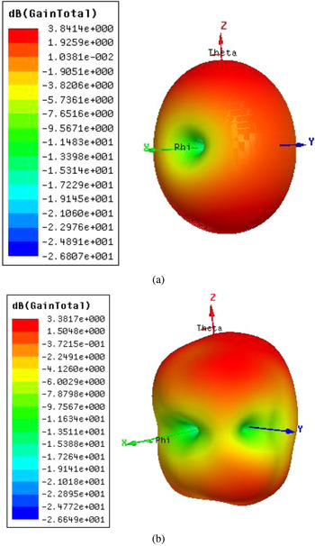
The final antenna has bi-directional and 3D pattern for 2.5 and 5.9 GHz, which is extracted by HFSS and shown in Fig. 10. As shown in Fig. 10, the antenna gains are 3.84 and 3.85 dBi at 2.5 and 5.9 GHz.
Antenna pattern for 2.5 and 5.9 GHz.

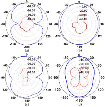
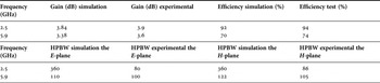
Figure 11 shows the measured radiation pattern of the antenna in phi = 0 and phi = 90 for 2.5 and 5.9 GHz for co- and cross-polarizations. Therefore, the prototype antenna shows a bi-directional pattern at both frequencies and our proposed design exhibits as an omni-directional in the H-plane. Radiation parameters that are compared between the simulation and experimental results are presented in Table 4 for 2.5 and 5.9 GHz.
The prototype antenna experimental pattern (a) phi = 0 at 2.5 GHz, (b) phi = 90 at 2.5 GHz, (c) phi = 0 at 5.9 GHz, and (d) phi = 90 at 5.9 GHz (solid line for co-polarization and dash line for cross-polarization).

Radiation parameters for second antenna, simulation, and experimental results.

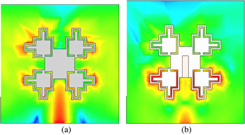
Figure 12 shows the antenna current distribution at two resonances at 2.5 and 5.9 GHz and as shown in Fig. 12(a), the current at 2.5 GHz is dispensed evenly in each unit cells, but the current is limited in lower unit cells at 5.9 GHz. By comparing Figs 12(a) and 12(b), it can be seen that the current is distributed in 50% of the unit cell in Fig. 12(b) comparing with Fig. 12(a). Therefore, it is expected that aperture effectively reduced to 50% and will reduce the efficiency.
The second antenna current distribution (a) 2.5 GHz and (b) 5.9 GHz.

C) Slot antenna with SRR load for CP
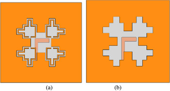
Finally, the modified feed line for making CP with slot antenna is discussed. So, as shown in Fig. 13, the L-shaped feed is used for achieving CP. Figure 13(a) shows the L-shaped feed with ring element and Fig. 13(b) shows the antenna in the absence of rings element and the results are compared together.
Slot antenna with bent feed line (a) with SRR load and (b) without SRR load.

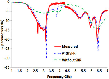
The final S-parameters of antenna simulation and measurement are compared in Fig. 14 and a good agreement between the results is visible. As shown in Fig. 14, when the antenna contains SRR; it has quad resonances at 2.5, 3.1, 5.95, and 6.35 GHz for quad band application at WLAN and WiMAX. However, in the absence of SRR, the antenna has only one resonance at 6.35 GHz. The results are compared with measurement results of the antenna with SRR load. The final antenna has 28, 8, and 7% bandwidth for 2.65, 5.95, and 6.35 GHz, respectively. In comparison, between Figs 14 and 9 we can see that the bent feed has less effect on S-parameters and bandwidth of the antenna.
S-parameter of the last antenna. Simulation in the presence and absence of SRR and experimental.

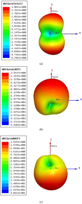
The final antenna has saved the bidirectional pattern and 3D pattern at 2.7 GHz, which is extracted by HFSS as a sample and shows in Fig. 15. In addition, the antenna, 3D pattern for LHCP (left hand CP) and RHCP (right hand CP) are shown in Figs 15(b) and 15(c), respectively. As shown here, the antenna gains are 4 dBi for total gain and 3.64 and 3.82 dBi for LHCP and RHCP at 2.7 GHz, respectively. Therefore, the prototype antenna shows CP.
Antenna pattern for 2.7 GHz (a) total gain, (b) LHCP gain, and (c) RHCP gain.

For the measurement quality of the CP field radiation is the axial ratio (AR). AR is the ratio of major and minor axes of the polarization along the bore-sight for the proposed antenna derived from the measured results on the fabricated antenna [Reference Kuhestani, Rahimi, Mansouri, Zarrabi and Ahmadian24].
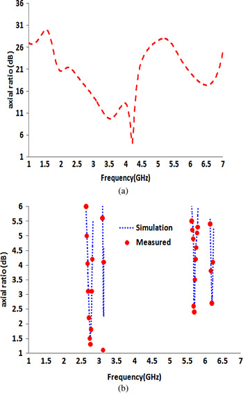
To compare and reveal the SRR loads effect of CP, the AR of antenna is presented in Fig. 16(a), where the antenna shows linear polarization.
The antenna AR for bent feed slot antenna (a) simulation result antenna in absence of SRR and (b) antenna in presence of SRR for simulation and experimental.

The measured AR result is presented in Fig. 16(b). The antenna has an AR of <3 in 2.8, 3 in 5.9 and 6.2 GHz and measurement results are confirmed the simulation with good agreement.
We have tested the antenna's horizontal and vertical fields at resonance frequencies to calculate the AR in the chamber room. The slot antenna AR comparison in the presence and absence of SRR is revealed that SRR elements that are helped to achieve CP.
As shown in Fig. 17, the current is distributed as a loop and it is caused CP at the resonance frequency. In fact, the bent feed line is activated the higher dominate mode in the antenna and this hybrid mode in antenna is caused CP. The effect of hybrid mode in antenna is appeared as loop in current distribution.
The second antenna current distribution at 2.8 GHz.

III. COMPARISON
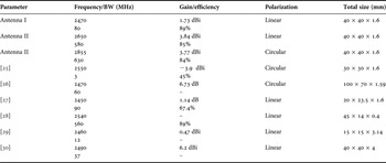
The miniaturization of antenna is one of the main reasons for using metamaterial structures. Despite of mentioned benefit, miniaturization with metamaterial usually is caused antenna gain reduction. One can find some comparisons between the current research and pervious one, which have been done here. Table 5 shows the miniaturization factor (size), gain, and efficiency and polarization comparisons.
Comparison for 2550 MHz.

For miniaturization, antenna with metamaterial and slots have been done some research with complementary SRRs and reactive impedance surface by Itoh and co-authors [Reference Dong, Toyao and Itoh31]. However, Itoh and co-authors [Reference Dong, Toyao and Itoh31] emphasize that by miniaturization with these techniques, the gain and efficiency are reduced drastically to −2 dBi and 25.5%, respectively, which are not given good radiation characteristic. In the first prototype antenna, we are achieved about 1.73 dBi and more than 89% for efficiency. By Oh and Sarbandi [Reference Oh and Sarbandi29], miniaturization with interdigital where they are reported negative or near zero gain (<0.5) and for matching of these antennas they emphasize on demand of a long taper line that increased the size of the antenna.
Metamaterial-Inspired Techniques for miniaturization are reported and they achieved more than 78% for miniaturization factor, but the antenna efficiency reduced to less than 28%, which made too much loss in antenna [Reference Ouedraogo, Rothwell, Diaz, Kazuko and Temme32]. On the other hand, all presented antennas have more bandwidth typically in comparison with the previous research as shown in Table 5.
IV. CONCLUSION
Two different Microstrip antennas based on the patch and slot forms are presented in this paper. Then the combination of EBG and SRR loads with fractal formation for miniaturization of microstrip antenna is noticed. We demonstrated the effect of Minkowski fractal on the EBG cells capacitance and patch antenna resonance in parallel.
At the second prototype antenna, we selected a slot antenna, which used SRR elements as a metamaterial load. We exhibit that by combination of fractal and SRR load, we are able to design dual-band antenna.
Finally, we presented another benefit of using SRR elements in slot antenna to achieve CP.
In this paper, it is shown that the antenna resonance could be predictable and measurable based on the initial structure, which has been done by the Minkowski fractal method.
 Mohammad Sadegh Sedghi was born in Tehran, Iran in 1983. He studied Telecommunication Engineering at the Gonabad Branch of Azad University in 2008. He just finished his master degree at Science and Research Branch of Islamic Azad University. He has more than 5 years of experience in GSM/WCDMA planning and optimization of mobile networks with Huawei vendor. He is currently working with the MTN group in Iran as a Radio Optimization Engineer and handling optimization tasks in WCDMA/LTE technology, which include 13 provinces/11 RNCs.
 Mohammad Naser-Moghadasi was born in Saveh, Iran, in 1959. He received the B.Sc. degree in Communication Engineering in 1985 from Leeds Metropolitan University (formerly Leeds Polytechnic), UK. Between 1985 and 1987 he worked as an RF design engineer for the Gigatech Company in Newcastle Upon Tyne, UK. From 1987 to 1989, he was awarded a full scholarship by the Leeds Educational Authority to pursue an M. Phil. studying in CAD of Microwave circuits. He received his Ph.D. in 1993, from the University of Bradford, UK. He was offered then a 2years Post Doc. To pursue research on Microwave Cooking of Materials at the University of Nottingham, UK. From 1995, he joined Islamic Azad University, at Science & Research Branch, Iran, where currently he is an Associate Professor and head of Telecommunications group. His main areas of interest in research are microstrip antenna, microwave passive and active circuits, RF MEMS. He is a member of the Institution of Engineering and Technology, MIET, and the Institute of Electronics, Information and Communication Engineers (IEICE). He has so far published over 160 papers in different journals and conferences.
 Ferdows B. Zarrabi was born in Babol, Iran, in 1983. He studied Electrical Engineering at the University of Tabriz in 2008, with a major in Communication Engineering. He was pursuing his M.S. at Tarbiat Modares University. His major areas of research interest are designing antennas for wireless and UWB applications for detecting breast cancer, radar and microwave devices, absorber, metamaterial, plasmonic, nano-antenna, cloak, photocell development, and THz antennas. He authored or co-authored more than 52 articles, and he published more than 34 ISI and Scopus indexed articles during 2013–2016. His current work focuses on fluid plasmonic and nano chain and particle with statistical optic for biosensing, based on nano-antenna, FANO resonance controlling with graphene and metasurface structures. He is also an invited reviewer of few ISI journals such as ACES, PIER, wireless personal communication, and few other journals.