I. INTRODUCTION
In the last decade, considerable progress has been made for organic semiconductor materials, especially for their use in solution-processed organic thin-film transistors (OTFTs).Reference Sirringhaus1–Reference Kang, Lee and Cho3 Some soluble small-molecule organic semiconductors were shown to afford high performance OTFTs whose device mobility of more than 10 cm2/Vs is generally higher than those obtained by vacuum-based thin-film processing. In most of these materials, π-electron cores, which are responsible for the semiconducting properties, are chemically substituted by alkyl chains (or other substituents) to obtain sufficiently high solubility for their use in the solution processes.Reference Ebata, Izawa, Miyazaki, Takimiya, Ikeda, Kuwabara and Yui4–Reference Shibata, Tsutsumi, Matsuoka, Minemawari, Arai, Kumai and Hasegawa9 It was shown that the substitution by normal alkyl chains is quite effective and useful, not only for improving the solvent solubility but also for enhancing the layered crystallinity. Particularly, the resultant high layered crystallinity should be most crucial to obtain high-performance OTFTs, as it allows the production of uniform channel semiconductor layers that have flat semiconductor/insulator interfaces, along which the efficient charge carrier transport takes place. Note that these substitution effects were also observed in high-mobility polymeric semiconductors that exhibit liquid crystalline phase and high layered crystallinity by long alkyl-chain substitutions.Reference McCulloch, Heeney, Bailey, Genevicius, Macdonald, Shkunov, Sparrowe, Tierney, Wagner, Zhang, Chabinyc, Kline, McGehee and Toney10
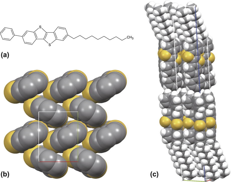
A particular example has been recently demonstrated in small-molecule organic semiconductors of 2-phenyl-benzothieno[3,2-b][1]benzothiophene (Ph-BTBT) substituted by normal alkyl chains [Ph-BTBT-Cm, Fig. 1(a)]: When the π-electron core of Ph-BTBT is substituted by sufficiently long alkyl chains (-CmH2m+1; m ≥ 5), the materials form bilayer-type layered-herringbone (LHB) packing whose bilayer unit is constructed by an antiparallelly aligned pair of polar monomolecular layers such that the adjacent phenyl groups are in contact in a head-to-head fashion [Figs. 1(b) and 1(c)].Reference Inoue, Minemawari, Tsutsumi, Chikamatsu, Yamada, Horiuchi, Tanaka, Kumai, Yoneya and Hasegawa6,Reference Minemawari, Tsutsumi, Inoue, Yamada, Kumai and Hasegawa11 In striking contrast, when the substituted alkyl chains are short (m < 5), Ph-BTBT-Cm exhibits different packing motifs other than the bilayer-type LHB.Reference Inoue, Minemawari, Tsutsumi, Chikamatsu, Yamada, Horiuchi, Tanaka, Kumai, Yoneya and Hasegawa6 The important fact is that the layered crystallinity is considerably enhanced in the bilayer-type LHB packing due to the separate formation of semiconducting π-electron-core layers and subsidiary alkyl-chain layers. A very similar trend is also observed in a series of mono-alkylated BTBT derivatives (mono-Cm-BTBTs).Reference Minemawari, Tanaka, Tsuzuki, Inoue, Yamada, Kumai, Shimoi and Hasegawa7 Furthermore, it was shown by the density functional theory calculations of the intermolecular interactions that the intralayer interactions between the alkyl chains contribute to stabilize the LHB-type molecular packing of the π-electron-core layers. These results demonstrate that the Ph-BTBT-Cm should be quite promising to achieve high performance solution-processed OTFTs because of its potential feasibility to produce large-area and uniform thin films with molecularly flat semiconductor/gate insulator interfaces due to the high layered crystallinity.Reference Mitsui, Okamoto, Yamagishi, Tsurumi, Yoshimoto, Nakahara, Soeda, Hirose, Sato, Yamano, Uemura and Takeya5,Reference Minemawari, Yamada, Matsui, Tsutsumi, Haas, Chiba, Kumai and Hasegawa12–Reference Janneck, Vercesi, Heremans, Genoe and Rolin19
(a) Molecular structure and (b and c) molecular packing motif of Ph-BTBT-C10.

As for the OTFT device productions, Iino, Usui, and Hanna have demonstrated that high-temperature spin-coating and a successive annealing process allow for obtaining polycrystalline thin films of Ph-BTBT-C10 that provide high performance OTFTs.Reference Iino, Usui and Hanna15 They claimed that the performance can be just enhanced by the change of film morphology, as associated with the structural phase transition from monolayer-type molecular packing to the bilayer-type molecular packing during the annealing process at elevated temperature reaching liquid crystalline smectic E phase. By contrast, we recently reported that fairly large-area single-crystalline thin films that have bilayer-type LHB packing can be produced in Ph-BTBT-C10 at around room temperature. Furthermore, we have shown that the formation of single-crystalline thin films with controllable layer number (n) thickness and exceptional homogeneity is possible by an elaborated blade-coating technique, as was confirmed by the atomic force microscopy (AFM) and the synchrotron X-ray diffraction experiments.Reference Hamai, Arai, Minemawari, Inoue, Kumai and Hasegawa20 The use of these single-crystalline thin films with various layer numbers affords us a unique chance to investigate the inherent transport characteristics of Ph-BTBT-C10. Actually, it was found that large access resistance (R acc) between the source/drain electrode and channel layer considerably affects the device characteristics. This effect is most probably ascribed to the inherent large anisotropy of carrier transport characteristics in Ph-BTBT-C10. It was discussed that the electrically inert alkyl-chain layers involved in the bilayer-type LHB packing in Ph-BTBT-C10 should be responsible for the large anisotropy of carrier conduction in our previous paper. Nonetheless, various effects, such as the features of layer-number-dependent nonlinear access resistance, their relation to the tunneling effects, and also the origin of observed current hysteretic behavior at the gate-off states, have not yet been revealed.
In this article, we discuss that the alkyl-chain layers in layered single-crystalline thin films of Ph-BTBT-C10 cause notable insulating effects in the operation of the single-crystalline OTFTs. The arguments are based on the experiments using single-crystalline OTFTs composed of channel layers with uniform bilayer number thickness over the whole channel areas and with variable layer number thickness between n = 1 and 15. The analyses on the layer number dependent device characteristics and gated-four-probe measurements revealed that the tunneling transport across the intrinsic insulating alkyl-chain layers causes large and nonlinear interlayer access resistance and thereby decrease of device mobility and increase of nonlinearity in the I d–V d characteristics. Intriguing effects due to the existence of highly insulating alkyl-chain layers were also seen at the gate-off states of the OTFTs as a hysteresis of measured voltages inside the OTFT channel region. Finally, we discuss the effect of nonlinear access resistance on OTFT characteristics with use of numerical simulation using a series of ideal OTFTs with various tunneling-based access resistances as a result of different layer number thicknesses, which rationalized the experimental results of the layer number-dependent device characteristics.
II. EXPERIMENT
Details of the device fabrications are similar with the previous report.Reference Hamai, Arai, Minemawari, Inoue, Kumai and Hasegawa20 We used heavily p-doped silicon wafer with thermally grown SiO2 layer (with a thickness of 100 nm) as substrates. They were cleaned by sonication for 3 min in each of deionized water, acetone, ethanol, and deionized water before use. A blade-coating technique was used to produce large-area single-crystalline thin films of Ph-BTBT-C10 with the use of the solution in chlorobenzene. We used a thin glass plate coated with Cytop (CTL-809M, Asahi Glass Co., Ltd., Tokyo, Japan) as the blade. The thickness of the single-crystalline thin films was roughly controlled both by the solution concentrations (ranged between 0.1 and 0.15 wt%) and by sweep rates (ranged between 1 and 3 μm/s). The sweep rate was controlled by a stepping motor (SHOT-302GS; SIGMA KOKI Co., Ltd., Hidaka, Japan). The obtained films are composed of large single-crystalline domains, each of which is composed of several distinct regions with different colors. The monocolored area corresponds to the film with a constant layer-number thickness, as described later.
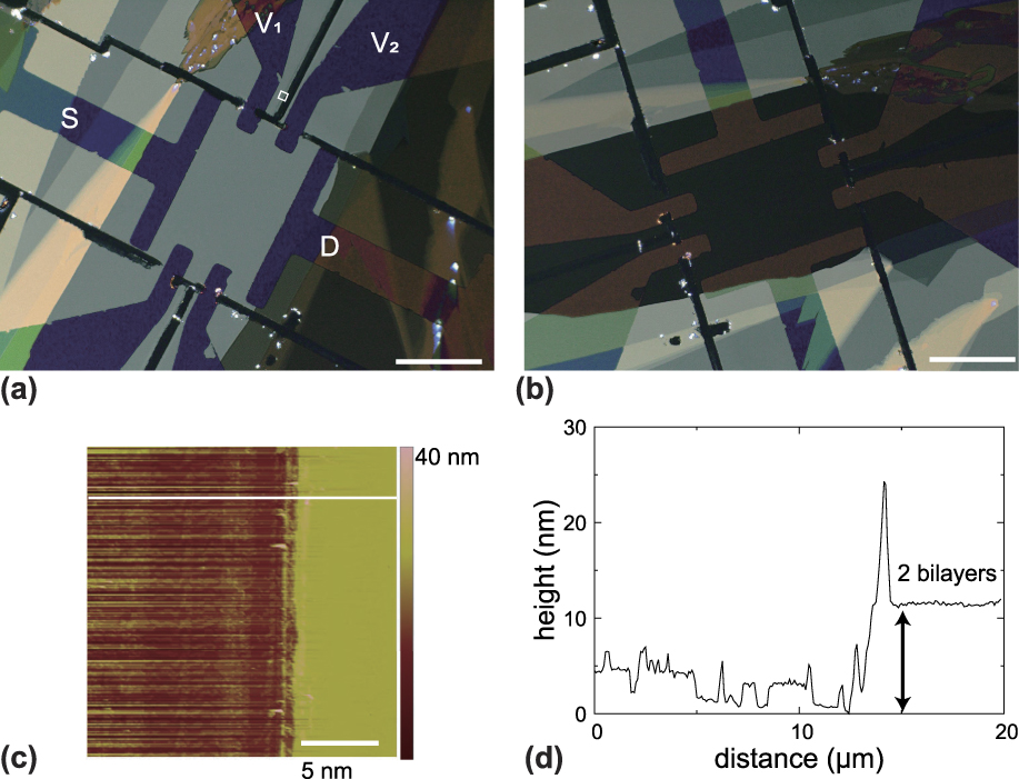
We fabricated single-crystalline OTFTs with bottom-gate top-contact geometry whose channel consisted of molecularly flat single-crystalline domain. An example of micrographs for the obtained single-crystalline thin film devices is shown in Figs. 2(a) and 2(b). Both the anisotropy and the thickness were characterized by using a polarized optical microscope. We can see clear changes of brightness with a rotation of 45° with the crossed-Nichols micrograph, indicating that the OTFT channel area is composed of one single-crystalline domain. Thickness and height profiles in the AFM measurements present the step-and-terrace structure with a uniform step height of the bilayer unit. An example for topography and height profile is shown in Figs. 2(c) and 2(d). In addition, the color of the film depends crucially on the bilayer number thickness, whose layer number was clearly identified by the AFM and X-ray diffraction measurements. We also found that the thickness of single-crystalline thin films was also consistent with the color analyses using Fresnel’s equation for multilayer films composed of an organic semiconductor thin film, a thermally grown transparent gate-dielectric silica layer with a thickness of 100 nm, and a doped silicon substrate. All the layer numbers of single-crystalline thin films shown in this article were identified by AFM measurements.
(a and b) Crossed-Nichols polarized micrographs for a single-crystalline Ph-BTBT-C10 thin film with constant layer-number thickness that is used as a channel layer of the OTFT for the gate-four probe measurements. Scale bar is 200 μm. (c) Step and terrace structure measured at the edge of single-crystalline thin film by AFM and (d) the corresponding height profile.

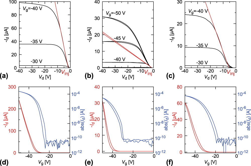
We produced single-crystalline OTFTs with bottom-gate top-contact geometry, by fabricating gold source/drain electrodes by vacuum deposition through a shadow mask (∼0.8 Å/s) on top of millimeter scale single-crystalline thin films with constant bilayer-number thickness. Thermal damage and/or metal penetration to the top surface layer during the metal deposition will complicate our analyses on the access resistance.Reference Dürr, Schreiber, Kelsch, Carstanjen, Dosch and Seeck21,Reference Xu, Liu, Sun, Balestra, Ghibaudo, Scheideler and Noh22 To suppress the possible damage, we used a vacuum evaporator equipped with a heat radiation shield near hot metal source and a circulation cooling system to control substrate temperature at 20 °C. For proper evaluation of the mobility, part of thin films outside the channel was trimmed away by using a micromanipulator (Micro Support Co., Ltd., Shizuoka, Japan). The OTFT characteristics were measured by one or a pair of two-channel source measurement units (Keysight Technologies, Santa Rosa, California B2912A) for the conventional two-probe and gated-four-probe measurements, respectively. In the measurement of transfer characteristics in the linear regime [Figs. 3(d)–3(f)], applied drain voltage (V d) was not unified for the films with different layer-number thicknesses because of the different injection voltage and V d-dependence of device mobilityReference Podzorov, Sysoev, Loginova, Pudalov and Gershenson23 due to nonlinear access resistance, as discussed later.
(a–c) Output characteristics and (d–f) transfer characteristics of OTFTs composed of Ph-BTBT-C10 single-crystalline thin films with channels of uniform layer number thickness, measured by two-probe measurements. Layer number is 3 for (a) and (d), 6 for (b) and (e), and 13 for (c) and (f). V d was set as −20 V for (d) and (e), and −30 V for (f). Note that the 2-probe measurements were performed with 4-probe FETs, in which the sense electrodes (overlap with channel layer: 50 × 50 μm2) were floating. Device geometry was L = 250 μm and W = 400 μm.

III. RESULTS AND DISCUSSION
A. Layer-number-dependent device characteristics
Figure 3 presents output characteristics of single-crystalline OTFTs composed of films with thickness of (a) 3 bilayers, (b) 6 bilayers, and (c) 12 bilayers. The device composed of the thinnest film showed nearly ideal I d–V d characteristics with very small nonlinearity, indicating that the interface resistance, or Schottky contact, between the Ph-BTBT-C10 single-crystalline thin film and gold electrode might be negligible.Reference Gundlach, Zhou, Nichols, Jackson, Necliudov and Shur24–Reference Minari, Darmawan, Liu, Li, Xu and Tsukagoshi27 On the other hand, the devices composed of relatively thick films showed highly nonlinear I d–V d characteristics. The nonlinear carrier injection was only observed in single-crystalline OTFTs composed of films with large n. It implies that some additional nonlinear resistance connected with the channel layer in series should exist within the layered single-crystalline films of Ph-BTBT-C10.
The layer number dependence was also apparent in the transfer characteristics, as presented in Figs. 3(d)–3(f). The device composed of a film with 3 bilayer thickness showed device mobility as high as 14 cm2/Vs, being comparable to the highest value for polycrystalline thin films.Reference Iino, Usui and Hanna15 However, the device composed of films with 6 bilayer thickness and 13 bilayer thickness showed a smaller device mobility of 3.2 cm2/Vs and 2.4 cm2/Vs, respectively. Such a trend—i.e., thicker films show larger nonlinearity in current–voltage characteristics and smaller device mobility—was found in all the single-crystalline devices which we investigated. Here, we use the TFT ideality factor, r, which was defined in Ref. Reference Choi, Cho, Frisbie, Sirringhaus and Podzorov28 as the ratio of the maximum channel conductivity experimentally achieved in a TFT to the maximum channel conductivity expected in an equivalent but ideal TFT with the claimed mobility and zero threshold voltage.Reference Choi, Cho, Frisbie, Sirringhaus and Podzorov28 The ideality factor of our OTFTs [31%, 15%, and 22% for Figs. 3(d)–3(f), respectively] is lower than unity because of the large threshold voltages. Thus, we investigated the device characteristics by using layer number n as the key parameter.
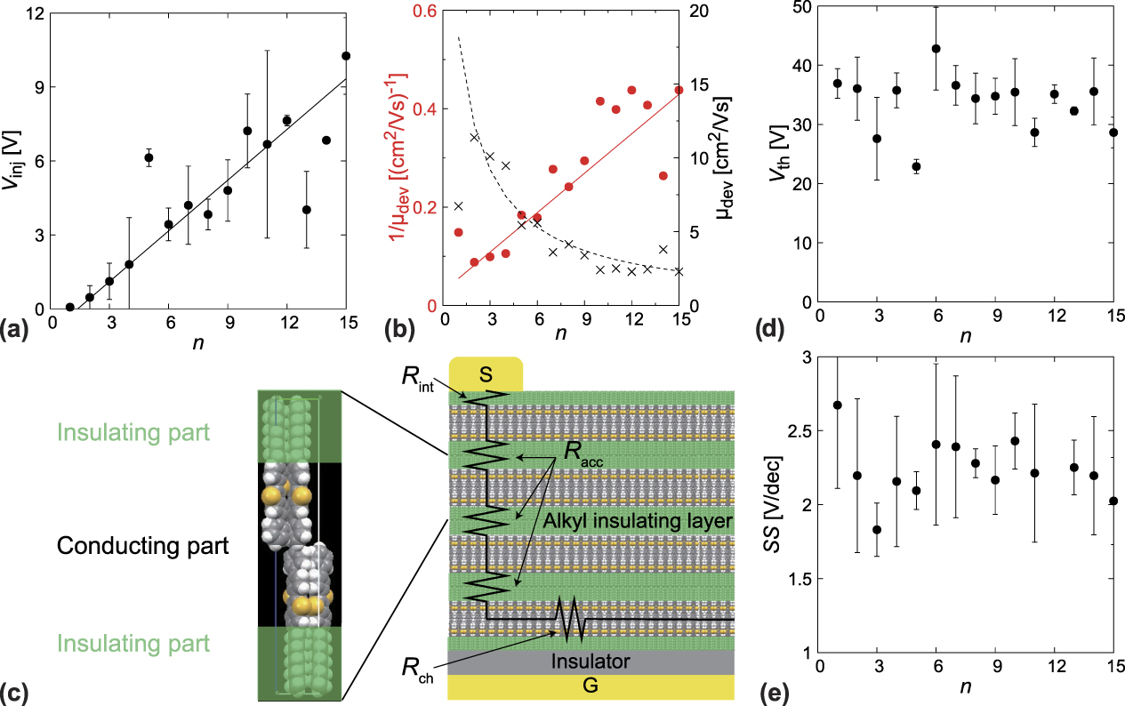
For the quantitative analysis of nonlinearity in current–voltage characteristics, we estimated injection voltage (V inj), which is defined as the intersection of linear fit for output characteristics with the voltage axisReference Torricelli, Ghittorelli, Colalongo and Kovacs-Vajna29 [see red lines in Figs. 3(a)–3(c)]. The value of V inj means the required voltage for effective carrier injection. Figure 4(a) plots the injection voltage as a function of layer number n. All the data shown in Fig. 4(a) were obtained at V g = −40 V. We found that the injection voltage linearly increases with the increase of the layer number by the following form:
 $${V_{{\rm{inj}}}}\left( n \right) = 0.67 \times \left( {n - 1} \right) \rm V\quad .$$
(a) Layer number dependence of injection voltage in OTFTs composed of Ph-BTBT-C10 single-crystalline thin films with channels of uniform layer number thickness, measured by two-probe measurements. All the data were obtained at V g = −40 V. (b) Layer number dependence of inverse device mobility in the linear regime. Device mobility is also shown by the broken line. (c) Schematic of the device showing the interlayer access resistance between channels and electrodes. (d) Threshold voltage and (e) subthreshold swings, both plotted as a function of the layer number.

This result is direct evidence that nonlinear current–voltage characteristics were induced by the layer-number-dependent nonlinear access resistance inside the semiconductor thin film, where the Schottky contact effect between the semiconductor layer and the electrode should be negligible.
Figure 4(b) shows layer-number dependence of the inverse device mobility in the linear regime (1/μ dev), which is proportional to the total resistance of the device. It is clear from the plot that the 1/μ dev is roughly proportional to the layer number. The result clearly indicates that the increase of the bilayer number leads to the increase of the total device resistance. Thus the decrease of the device mobility (or increase of the inverse device mobility) can be described by the following equations:
 $$\imu _{{\rm{dev}}}^n = { {\imu} _{{\rm{dev}}}^1} / {\left[ {1 + \itheta \left( n \right)} \right]}}\quad$$
or
 $${1 / {\imu _{{\rm{dev}}}^n}} = {1 / {\imu _{{\rm{dev}}}^1}} + {{\itheta \left( n \right)} / {}}\imu _{{\rm{dev}}}^n\quad ,$$
where  $\imu_{{\rm{dev}}}^n$ denotes the device mobility of the n bilayer film in the linear regime and θ(n) denotes the mobility attenuation factor defined by the ratio of layer-number-dependent access resistance
 $\left( {R_{{\rm{acc}}}^n} \right)$ to the total resistance of the ideal single bilayer device, in which the access resistance can be ignored and carriers have same conduction properties as thicker films, respectively. The following parameters are used to fit the experimental results by Eq. (3) [the calculated value is shown by the solid line in Fig. 4(b)]:
 $$\imu _{{\rm{dev}}}^1 = 18.0\;{{{\rm{c}}{{\rm{m}}^2}} / {{\rm{V}}{\rm{s}}}}\quad ,$$
 $$\theta \left( n \right) = 0.47 \times \left( {n - 1} \right)\quad .$$
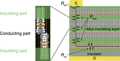
These results demonstrate that the layer-number-dependent access resistance due to the interlayer carrier transport should take crucial roles in the device operations. Figure 4(c) shows the schematics of the interlayer carrier transport: In the layered single-crystalline thin films of Ph-BTBT-C10, electrically inert alkyl-chain layers and semiconductive π-electron core layers are formed and alternately stacked in the bilayer-type LHB packing.Reference Yamagishi, Noda, Kobayashi and Yamada30 The inserted alkyl chain layers between semiconductive π-electron core layers should drastically suppress the conductivity in the interlayer direction. Therefore, the multiple alkyl-chain layers between the channel layer and the source/drain electrodes will work as a large access resistance in single-crystalline OTFTs with the staggered device geometry. This picture is well consistent with the layer number dependent injection voltage and device mobility in the form of (n − 1) as presented in Eqs. (1) and (5); the number of paired alkyl chain layers is equal to n − 1 in the single-crystalline thin films with n bilayer thickness. The top film surface is also covered by the unpaired alkyl-chain layer but the thickness is only half of the paired alkyl chain layers. Hence, it is most probable that the conduction across the paired alkyl chain layer causes the nonlinear interlayer access resistance, whereas the unpaired alkyl chain layer on the top film surface can be ignored. With this assumption, single-crystalline transistor with coplanar geometry is expected to have negligible access resistance. However, we found that bottom-contact devices based on the Ph-BTBT-C10 single-crystalline thin film show smaller device mobility (less than 1 cm2/Vs) and larger nonlinear I d–V d characteristics than the top-contact devices. We speculate that the additional large parasitic resistance should be caused in the coplanar-type bottom-contact devices, which is derived from the different geometrical configuration of the electrode and the Ph-BTBT-C10 single-crystalline thin film (that involves highly insulating and intrinsic alkyl-chain layers), compared to the staggered-type top-contact devices. Hence, the comparison between top-contact device and bottom-contact device is not straightforward.
In the analyses of the injection voltage and the device mobility, we assumed that the transport properties along the channel layer should be unaffected by the layer number. Figure 4 shows the threshold voltage (Vth) [Fig. 4(d)] and subthreshold swing (SS) [Fig. 4(e)], plotted as a function of the layer number, respectively. The values of the threshold voltage and subthreshold swing are larger than those expected for the ordered single crystalline active layer and comparable to those for polycrystalline devices reported in the literature.Reference Iino, Usui and Hanna15 We consider that deep trap levels should be associated with the obtained large threshold voltage and subthreshold swing; these trap levels should come from such as silanol groups at the semiconductor/dielectric layer interface and/or possible Schottky barrier at the semiconductor/electrode interface. Actually, no layer-number dependence was observed in both threshold voltage and subthreshold swing. It indicates that the increase of the layer number causes only the increase of access resistance at least for n ≥ 2. It is interesting to point out that the layer-number dependence does not hold for n = 1. The origin of small device mobility for n = 1 is probably due to the scattering derived from crystal defect, absorbed molecules, or phonons, the effect of which should be considerably enhanced for the carrier transport inside the ultrathin semiconductor layer with n = 1.Reference Peng, Huang, Zhou and Chan17,Reference Takagi, Koga and Toriumi31
B. Access resistance and gated-four-probe characteristics
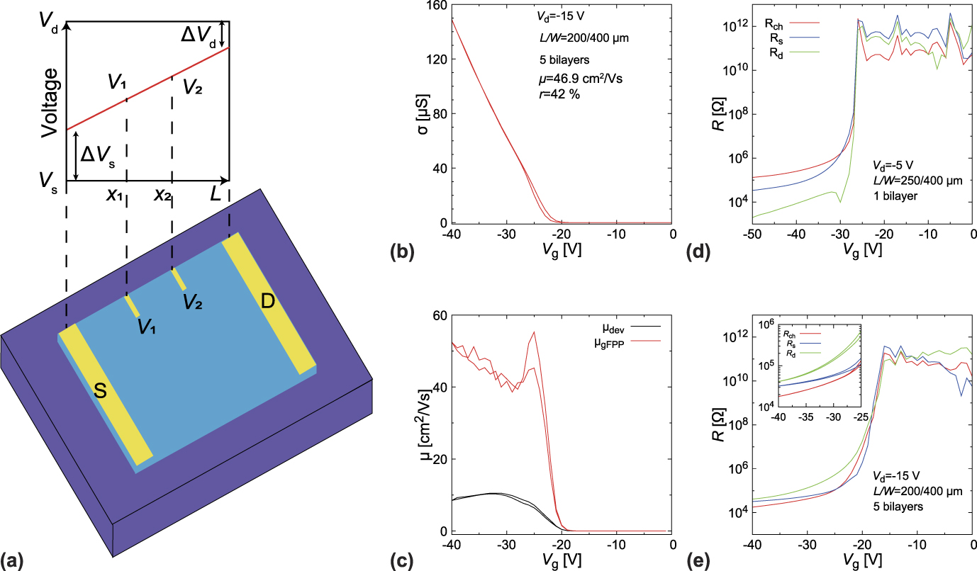
We used the gated-four-probe technique to investigate the contribution of intra- and interlayer conductions to the device characteristics separately.Reference Podzorov, Sysoev, Loginova, Pudalov and Gershenson23,Reference Podzorov, Pudalov and Gershenson32–Reference Uemura, Rolin, Ke, Fesenko, Genoe, Heremans and Takeya36 By the technique, it becomes possible to discriminate between the transports along channel layer and the parasitic resistance at source and drain electrodes, quantitatively. For this purpose, a pair of sense electrodes in addition to a usual OTFT device structure is only necessary, and no other special equipment is required. Figure 5(a) shows the schematic of the gated-four-probe technique. The potential measurements at the two points inside the transistor channel [V 1, V 2 in Fig. 5(a)] allow us to obtain the channel conductance σ by the equation: σ = I d/ΔV = I d/(V 2 − V 1). We can also evaluate, separately, the potential drop between the channel layer and the source electrode (ΔV s) and that between the channel layer and the drain electrode (ΔV d), by extrapolating the potential gradient to the channel edge, as
 $${\rm{\Delta }}{V_{\rm{s}}} = {V_1} - {{{V_2} - {V_1}} \over {{x_2} - {x_1}}}{x_1}\quad ,$$
 $${\rm{\Delta }}{V_{\rm{d}}} = {V_{\rm{d}}} - {{{V_2} - {V_1}} \over {{x_2} - {x_1}}}(L - {x_2})\quad ,$$
where x 1, x 2, and L are the lengths from the source electrode to the first sense probe, to the second sense probe, and to the drain electrode, respectively [see Fig. 5(a)]. The access resistances at the source (R s) and the drain (R d) electrodes are obtained by dividing ΔV s and ΔV d by I d, as
 $${R_{\rm{s}}} = {{\Delta {V_{\rm{s}}}} / {{I_{\rm{d}}}}}\quad ,$$
 $${R_{\rm{d}}} = {{\Delta {V_{\rm{d}}}} / {{I_{\rm{d}}}}}\quad .$$
(a) Schematic of the gated-four-probe measurement. (b) Gated-four-probe transfer characteristic of an OTFT composed of Ph-BTBT-C10 single-crystalline thin films with channels of 5 bilayer thickness. (c) V g dependence of four-probe mobility and device mobility in the linear regime. (d and e) V g dependence of R s, R d, and R ch obtained with the device composed of a channel with (d) 1 bilayer thickness and (e) 5 bilayer thickness. The inset of (e) shows V g dependence of R s, R d, and R ch. Note that the values of R s and R d in the off-state are plotted without any correction by using measured V 1, V 2, and drain current. So the off-state resistance may contain artifacts due to the precision of the measurement.

Note that the width of sense electrodes of the devices is not negligible, which might cause a shunt current and might result in the overestimation of channel mobility. However, we can ignore the possibility of the mobility overestimation, considering the device model presented in Sec. III.C: the nonlinear access resistance between the channel layer and the sense electrode should prevent the shunt current.
Figure 5(b) shows a gated-four-probe transfer characteristic of the device composed of a film with 5 bilayer thickness, which exhibited the highest four-probe mobility (μ gFPP), reaching as high as 46.9 cm2/Vs. The four-probe mobility obtained by the slope of the transfer characteristics exceeded 40 cm2/Vs for a wide V g range [Fig. 5(c)] and is not an artifact derived from the large parasitic resistance,Reference Uemura, Rolin, Ke, Fesenko, Genoe, Heremans and Takeya36–Reference Bittle, Basham, Jackson and Jurchescu38 although this value is even much larger than that we obtained through the analysis of the layer-number-dependent (two-probe) device mobility. We here note that the TFT ideality factor r is 42% simply because of the large threshold voltage; r is comparable to the ratio of the maximum effective gate bias |V g − V th|max (=17 V) to the maximum gate bias |V g|max. Fig. 5(e) shows the gate voltage dependence of R ch, R s, and R d, as defined above. Both R s and R d showed larger values than R ch. The high four-probe-mobility and large access resistance imply that the device mobility is considerably suppressed to a much lower value (less than 20 cm2/Vs) by the large interlayer access resistance, despite the excellent transport characteristics within the semiconductive π-electron core layers in the single-crystalline Ph-BTBT-C10 thin films revealed by the gated-four-probe measurement.
Figure 5(d) presents the V g dependence of R ch, R s, and R d of the devices composed of 1 bilayer thickness and 5 bilayer thickness. It is clear that the device composed of a film with 1 bilayer thickness presents much smaller access resistance than the device composed of a film with multilayer thickness [Fig. 5(e)]. The result also indicates that the access resistance originating from the unpaired alkyl-chain layer on the top single-crystalline film surface does not considerably affect the device characteristics, whereas the (n − 1)-dependence of injection voltage and device mobility is ensured. Relatively large R s, as compared to R d, of the devices composed of films with 1 bilayer thickness observed in Fig. 5(d) might be attributed to the effect of the Schottky barrier, which cannot be ignored because of very small access resistance.
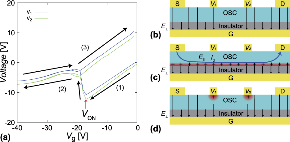
Figure 6(a) shows the voltages measured at both of the sense electrodes (V 1 and V 2), as a function of V g during the forward and backward sweeps of V g between 0 V and −40 V [the data correspond to the measurement for Fig. 5(b)]. We observed considerable hysteretic behavior between the forward and backward sweeps at the gate-off state. The following features are observed: In the forward sweep from V g = 0 V to V g = V on, V 1 and V 2 start at 0 V and linearly decrease until V g reaches the onset voltage (V on) [(1) in Fig. 6(a)]. Similarly, in the backward sweep from V g = V on to V g = 0 V, V 1 and V 2 linearly increase with the change of V g, starting from the value at V g = V on [(3) in Fig. 6(a)]. In the gate-off state, similar gate-voltage dependence of V 1 and V 2 was commonly observed. By contrast, when V g is smaller than V on [or |V g| is larger than |V on|, (2) in Fig. 6(a)], the channel layer is conductive so that the V 1 and V 2 should be determined by the potential at the channel just below the sense electrodes, because of the negligible current between the channel layer and the sense electrodes [Fig. 6(c)], and showed small hysteresis. However, when V g is larger than V on [|V g| is less than |V on|, (1) and (3) in Fig. 6(a)], the channel layer at the gate-off state becomes also insulating. In the gate-off state, the changes in V 1 and V 2 under the sweep of V g are proportional to the change in V g, as can be seen in Fig. 6(a). We consider that the hysteretic behavior could be ascribed to the difference of the electrical potential at V 1 and V 2 between before and after the channel becomes gate-on-state during the V g sweep. Once the channel becomes on-state, some residual charges will remain at or below the sense electrodes [Figs. 6(b) and 6(d)], which may easily affect the electrical potential at V 1 and V 2.Reference Moscatello, Castaneda, Zaidi, Cao, Usluer, Briseno and Aidala39 A similar insulating effect derived from the alkyl insulating layer in the OTFT was reported by Yamagishi et al.Reference Yamagishi, Noda, Kobayashi and Yamada30 for the crystalline thin film of diC8-BTBT with bottom-gate bottom-contact geometry, where Kelvin-force probe microscopy revealed that the adjacent semiconductive layers were electrically isolated by the alkyl chain layer.
(a) V g dependence of measured voltage at sense electrodes of V 1 and V 2 for an OTFT composed of Ph-BTBT-C10 single-crystalline thin films with channels of 5 bilayer thickness; data correspond to the measurements shown in Fig. 5(b). (b–d) Schematics for the electric field distribution inside the device (b) at the gate-off state with the decrease of V g above V on, (c) at the gate-on state, and (d) at the gate-off state with the increase of V g above V on as shown in (a).

C. Model simulation of tunneling-based access resistance
Based on the analyses of layer-number-dependent OTFT characteristics in the above, we have demonstrated that the single-crystalline Ph-BTBT-C10 thin films exhibit highly anisotropic carrier transport, where the conduction perpendicular to the layered crystal surfaces presents highly nonlinear current–voltage characteristics, as is characterized by the layer number dependence of V inj. A similar example of nonlinear I d–V d characteristics is caused by the Schottky barrier, which is described by Fowler–Nordheim tunneling through potential barrier between the electrode and semiconductor layer. In the present case, the insulating alkyl-chain layer, as schematically presented in Fig. 4(c), should form a high potential barrier against carrier injection from the electrode to the channel layer. If the barrier height is much higher than the thermal energy at room temperature (about 26 meV), the carrier motions through the insulating alkyl-chain layers should take place in a tunnel-like manner.
It is generally known that the tunneling transport obeys exponential dependence on the inverse of the barrier width. It means that a paired alkyl-chain layer within the single-crystalline film should give much larger tunneling resistance than an unpaired alkyl chain layer on top of the film surface. So we adopt a model for access resistance derived from the series (n − 1) tunneling resistance and neglect the tunnel resistance derived from the unpaired alkyl chain layer on top of the film surface. This assumption is well consistent with the experimental (n − 1) dependence of both injection voltage [Eq. (1)] and device mobility [Eqs. (3)–(5)].
To simulate the I d–V d characteristics of the single-crystalline OTFT, we used the Simmons equation for describing the I–V characteristics of the tunneling resistance [Eq. (27) in Ref. Reference Simmons40].
 $${I_{{\rm{tunnel}}}} = {{eS} \over {2\pi h{d^2}}}\left\{ {\left( {{\iphi _0} - {{eV} \over 2}} \right)\exp \left[ { - {{4\pi d} \over h}{{\left( {2{m^ * }} \right)}^{{1 \over 2}}}{{\left( {{\iphi _0} - {{eV} \over 2}} \right)}^{{1 \over 2}}}} \right] - \left( {{\iphi _0} + {{eV} \over 2}} \right)\exp \left[ { - {{4\pi d} \over h}{{\left( {2{m^ * }} \right)}^{{1 \over 2}}}{{\left( {{\iphi _0} + {{eV} \over 2}} \right)}^{{1 \over 2}}}} \right]} \right\}\quad ,$$
where m*, ϕ 0, d, and S denote effective mass, barrier height, barrier width of tunneling barrier, and effective area for carrier injection, respectively. We here considered that only paired alkyl chain layers work as the tunneling barrier with an assumption of the parameters as m* = m e, ϕ 0 = 1.0 eV, and d = 20 nm. The barrier width is derived from the crystal structure of Ph-BTBT-C10,Reference Minemawari, Tsutsumi, Inoue, Yamada, Kumai and Hasegawa11 and other tunneling barrier parameters are consistent with the previous reports on tunneling molecular junctions based on alkanethiol self-assembled monolayers.Reference Wang, Lee and Reed41–Reference Salomon, Shpaisman, Seitz, Boecking and Cahen44 The effective area for carrier injection, S, was set to be 50 × 400 μm2, by considering the principal area of source and drain electrodes. We ignored the distribution of vertical current density under the electrodes and current crowding effect.Reference Richards and Sirringhaus45 Under the uniform current density assumption, we could simplify the model OTFT device with tunneling access resistance, as described by Eq. (10), which is connected to the channel of the OTFT in series [see Fig. 4(c)]. We also reasonably assumed that the band structure should be the same for all the semiconductive π-electron core layers of paired Ph-BTBT’s so that the respective alkyl-chain layers should afford same voltage drops.
In the simulation, we optimized the potential drop in the alkyl insulating layers (ΔV) for the each set of the parameters (n, μ ch, V d, and V g), where μ ch denotes the mobility in the OTFT channel layer. We assumed ΔV = ΔV d + ΔV s and the potential drop for each insulating layers the same. For ΔV = 0, I tunnel becomes 0. To flow current into the OTFT channel layer, ΔV should have non-zero value and I tunnel monotonically increases with the increase of ΔV. If ΔV is too large or V d − ΔV (the voltage applied to the channel layer) is too small, the current inside the channel layer (I FET) would be smaller than I tunnel and the channel resistance would dominate the drain current in the model device. In a steady current state of the real devices, the current flowing in the tunnel resistance and OTFT channel layer should be the same due to the conservation law of charge. Therefore, the current of the model device, where the channel and the tunnel resistances are connected in series, can be determined by equating the current through the two part of the model device; I tunnel (ΔV, n) = I FET (V d − ΔV, V g, μch), which is explicitly shown in the following:
 $$\matrix{ {{e \over {2\pi h{d^2}}}S\left\{ {\left( {{\iphi _0} - {{e\Delta V} \over {2n}}} \right)\exp \left[ { - {{4\pi d} \over h}{{\left( {2{m^ * }} \right)}^{{1 \over 2}}}{{\left( {{\iphi _0} - {{e\Delta V} \over {2n}}} \right)}^{{1 \over 2}}}} \right] - \left( {{\iphi _0} + {{e\Delta V} \over {2n}}} \right)\exp \left[ { - {{4\pi d} \over h}{{\left( {2{m^ * }} \right)}^{{1 \over 2}}}{{\left( {{\iphi _0} + {{e\Delta V} \over {2n}}} \right)}^{{1 \over 2}}}} \right]} \right\}} \cr { = \left\{ {\matrix{ {{L \over W}{\imu _{{\rm{ch}}}}{C_{\rm{i}}}\left( {{V_{\rm{g}}} - {V_{{\rm{th}}}} - {{{V_{\rm{d}}} - \Delta V} \over 2}} \right)\left( {{V_{\rm{d}}} - \Delta V} \right)} \hfill & {{V_{\rm{g}}} - {V_{{\rm{th}}}} - \left( {{V_{\rm{d}}} - \Delta V} \right) > 0} \hfill \cr {{L \over {2W}}{\imu _{{\rm{ch}}}}{C_{\rm{i}}}{{\left( {{V_{\rm{g}}} - {V_{{\rm{th}}}}} \right)}^2}} \hfill & {{V_{\rm{g}}} - {V_{{\rm{th}}}} - \left( {{V_{\rm{d}}} - \Delta V} \right) \lt 0} \hfill \cr} } \right.} \cr} \quad .$$
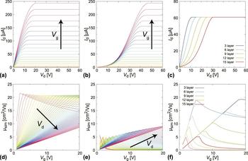
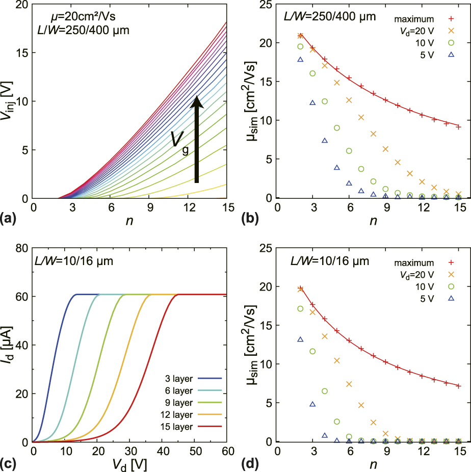
Figures 7(a) and 7(b) show the simulated I d–V d characteristics of the model device at μ ch = 20 cm2/Vs, L/W = 250/400 μm, C i = 34.5 nF/cm2, and V g − V th ranged between 1 and 20 V with a step of 1 V. The simulated curves for n = 2 [Fig. 7(a)] presented conventional I d–V d characteristics with negligible nonlinearity, but the simulated curves for n = 15 [Fig. 7(b)] presented large nonlinearity: Experimental results of the layer-number-dependent nonlinearity, shown in Figs. 3(a)–3(c), were qualitatively reproduced by using the tunneling resistance with the reported parameters. Figure 7(c) summarizes the I d–V d characteristics of n = 3, 6, 9, 12, and 15 for V g = 10 V. The nonlinearity and thus injection voltage increase monotonically with the increase of the layer number. By fitting the linear part, we calculated the injection voltage for simulated I d–V d curves. Figure 8(a) shows the injection voltage for various V g, ranged between 1 and 20 V, plotted as a function of the layer number. For large V g (larger than 10 V), the injection voltage increased almost linearly with the increase of the layer number, as is consistent with the experiment. The linear increase of V inj with the increase of the layer number can be interpreted as the clear evidence that access resistance per 1 bilayer is independent of the layer number, as discussed later. The injection voltage calculated for V g = 8–10 V is quantitatively consistent with the experimental layer-number dependence of the injection voltage. Note that I d is same in the saturation regime of this model device, irrespective of layer number n. The tunneling resistance only causes the decrease of V d − ΔV which is a part of drain bias and is practically applied to the channel layer. Hence, the I d in the saturation regime (where sufficiently large drain bias is applied to the channel layer) does not depend on the drain bias by definition, despite the notable injection voltage and shift of pinch-off point. This is consistent with our experimental results; mobility attenuation factor theta, θ(n), in the saturation regime is smaller than that in the linear regime.
(a and b) Simulated I d–V d characteristics of the model device with the channel layer number thickness of (a) 2 and (b) 15, with a channel mobility of 20 cm2/Vs, L/W = 250/400 μm, C i = 34.5 nF/cm2, and V g − V th ranged between 1 and 20 V with a step of 1 V. (c) I d–V d characteristics of the model devices for layer number thicknesses of 3, 6, 9, 12, and 15 at V g = 10 V. (d and e) Simulated device mobility of the model device with the channel layer number thickness of (d) 2 and (e) 15, in the linear regime plotted as a function of V g, for various V d ranged between 1 and 50 V with a step of 1 V. (f) Simulated device mobility as a function of V d in the linear regime with various channel layer number thicknesses of 3, 6, 9, 12, and 15 bilayers, for V g = 5 V (broken curves) and 20 V (solid curves).

(a and b) Simulated layer number dependence of (a) injection voltage and (b) device mobility for the model device using same parameters with Fig. 7. (c and d) Simulated device characteristics for short channel device with L/W = 10/16 μm; (c) output characteristics of the devices with various channel layer number thicknesses of 3, 6, 9, 12, and 15 bilayers, and (d) layer number dependence of device mobility calculated at V d = 5, 10, and 20 V, and also of the maximum calculated device mobility.

Our model simulation also reproduced the layer-number dependence of device mobility. Figures 7(d) and 7(e) show the simulated device mobility in the linear regime (μ sim) for V d ranged between 1 and 50 V with a step of 1 V as a function of V g. We have simply defined μ sim as μ sim = (L/WC iV d)(δI d/δV g) for all the data because I d in the saturation regime is independent of the layer number. Due to the definition, which is valid only for the linear regime, the transition between the linear regime and saturation regime (at V g = V d − ΔV) appeared as kinks with maximal values in Figs. 7(d) and 7(e). For V g smaller than the kink, or in the saturation region, μ sim linearly increased, due to the factor of [V g − V th − (V d − ΔV)/2] in μ sim. On the other hand, μ sim monotonically decreased for V g larger than the kink, or in the linear regime. This behavior should be due to the effect of the tunnel resistance: The tunnel resistance becomes more dominant and ΔV becomes larger at larger V g, which gives smaller channel resistance. The increase of ΔV, or the decrease of applied bias for channel resistance (V d − ΔV), causes the decrease of μ sim because the tunnel resistance becomes more dominant at large V g that gives small channel resistance. The notable feature of μ sim for n = 2 [Fig. 7(d)] is that μ sim around the maximal values is almost same for all the values of V d and exceed the channel mobility of 20 cm2/Vs. This result indicates that with exponentially varying parasitic resistance, the device mobility obtained by the slope of the I d–V g curve may be overestimated due to the rapidly decaying parasitic resistance. This simulated result is consistent with the recent experiment, which demonstrated that the device mobility can be overestimated due to the nonlinearly decaying parasitic resistance.Reference Uemura, Rolin, Ke, Fesenko, Genoe, Heremans and Takeya36,Reference Bittle, Basham, Jackson and Jurchescu38 On the contrary, the simulated mobility for n = 15 [Fig. 7(e)] showed smaller mobility than that for n = 2 [Fig. 7(d)] and different V g dependences. For small V d (about less than V inj), μ sim is close to 0, reflecting the small-current region in I d–V d characteristics [Fig. 7(b)]. The maximal value of μ sim is also suppressed due to the series tunneling resistance, especially for small V d. This distinctive feature of μ sim, largely depending on both V d and V g for the thicker film, gives rise to ambiguity for the experimental estimation of the μ dev value. From the reason, it is rationalized that in our experiments, we used μ dev which is obtained by a transfer curve with unusually large V d whose mobility showed the smallest V g dependence and large value.
Figure 7(f) shows μ sim as functions of V d, for V g = 5 V (broken) and 20 V (solid), and n = 3, 6, 9, 12, 15. We can clearly see that μ sim is largely dependent on V d and monotonically decreased with the increase of the layer number. For n more than 9, μ sim dropped to zero at large V g. To elucidate the layer-number dependence of simulated mobility, we plotted μ sim as a function of n in Fig. 8(b). μ sim for fixed V d values as 5 V (blue), 10 V (green), and 20 V (orange) showed monotonic decrease and almost zero at sufficiently large n. The abrupt decrease of μ sim especially for small V d is derived from the increase of V inj. Due to large V inj for large n, the appropriate V d for evaluating mobility is not the same for devices with different layer numbers, as mentioned above. To compare μ sim in the linear region without the influence of nonlinearity, we plotted the maximum values of μ sim at V g = 20 V for each layer number in Fig. 8(b) by red crosses. The maximum value showed moderate layer number dependence compared to other plots in Fig. 8(b) and can be characterized by the same equations as experimental layer number dependence [Eq. (2)] with fitting parameters μ0 = 23.4 cm2/Vs and θ = 0.085. The success of the fitting by Eq. (2) indicates that at the parameters which gives maximum μ sim, an assumption we made to model the layer-number dependent device characteristics—i.e., ΔV per 1 bilayer and hence the interlayer access resistance per 1 bilayer are almost independent of the layer number—is reasonably rationalized. The effect of the nonlinear series resistance should become more apparent in short channel devices, as the ratio of the channel resistance to the access resistance becomes smaller. Figure 8(c) shows the I d–V d characteristics for L/W = 10/16 μm and V g = 10 V. In the simulation, the ratio of channel length and width and the value of channel resistance were taken as the same with those of the long-channel device described in Fig. 7, whereas the ratio of the channel resistance to device resistance was only decreased. In the short channel device, the I d–V d curve showed notable nonlinearity even for the n = 3 device, implying that the low-voltage operation in small-channel devices becomes very difficult in high-mobility single-crystalline OTFTs with alkyl-substituted organic semiconductors. Additionally, μ sim at fixed V d [5, 10, and 15 V, in Fig. 8(d)] showed a smaller value than those in the long-channel device [Fig. 8(b)], reflecting the larger V inj in the small-channel device. On the other hand, the maximum values of μ sim for V g = 20 V [Fig. 8(d)] showed almost same values with those for long-channel devices shown in Fig. 8(b). The feature is related to the nonlinear access resistance as is caused by the tunneling: For short channel devices, injection voltage should be larger than that of long channel devices, whereas the difference of injection voltage per 1 bilayer is not so large because small change of voltage applied to the tunneling resistance will efficiently suppress the access resistance. Hence, the device mobility is not affected by the scale of the device.
IV. CONCLUSIONS
We have experimentally and theoretically investigated the effects of tunneling-based access resistance on device characteristics due to the conduction across the highly insulating and intrinsic alkyl-chain layers of single-crystalline Ph-BTBT-C10 thin films. The device mobility and nonlinear current–voltage characteristics exhibit notable layer-number (n) dependence where the device resistance is proportional to the layer number. We have demonstrated that the increase of the device resistance was caused by nonlinear interlayer access resistance due to the tunneling transport across the alkyl insulating layers within the single-crystalline thin films. The gated-four-probe measurements demonstrated the very large access resistance and very high mobility reaching as high as 48.1 cm2/Vs in single-crystalline thin films of Ph-BTBT-C10. Simulated OTFT characteristics based on tunneling-based nonlinear access resistance well reproduced the experimental layer-number dependent device characteristics that can be characterized by simulated device mobility and nonlinear I d–V d characteristics. The simulation also showed that the low-voltage operation of the high mobility OTFT with single-crystalline thin film of alkyl-substituted organic semiconductor materials is difficult. We consider that the uncontrolled nature of the film thickness and resultant variability of enormous access resistance, as demonstrated in this study, should be one of the reasons for the large distribution of device performance in the single-crystalline OTFTs that have been reported so far.Reference Mitsui, Okamoto, Yamagishi, Tsurumi, Yoshimoto, Nakahara, Soeda, Hirose, Sato, Yamano, Uemura and Takeya5,Reference Minemawari, Yamada, Matsui, Tsutsumi, Haas, Chiba, Kumai and Hasegawa12,Reference Diao, Tee, Giri, Xu, Kim, Becerril, Stoltenberg, Lee, Xue, Mannsfeld and Bao18
ACKNOWLEDGMENTS
We are grateful to Nippon Kayaku Co., Ltd., for providing starting materials of BTBT. We are also grateful for the collaborations with Dr. Satoru Inoue (Nippon Kayaku Co., Ltd.) in the syntheses of Ph-BTBT-C10, with Dr. Hiromi Minemawari (AIST) in the semiconductor thin-film fabrication, and with Prof. Reiji Kumai (KEK) in the thin-film characterization by x-ray diffractions. This study was partly supported by JSPS KAKENHI Grant Numbers JP17H05144, JP17K14370, JP18H03875, from the Japan Society for the Promotion of Science (JSPS).