Introduction
A hallmark of the development of civilization is the organization of manufacturing and technology. Societies until the 18th century were largely dominated by small manufacturing by individual artisans and craftsmen, with a single person possessing the skills and experience for a full fabrication cycle. The early 20th century saw a transition to production line fabrication, with rigorously enforced standards and an increased focus on skillsets of individual workers. By the second half of the 20th century, the rapidly emerging trend was continuous automation and later robotization, giving rise to multibillion dollar large-volume industries.
Today, the combination of emerging computer-guided design and three-dimensional (3D) printing technologies are enabling new types of fabrication based on individual designs, where high complexity structures can be fabricated at low cost and in small numbers. It is argued that a combination of 3D manufacturing and technologies underlying the “Internet of things” can lay the foundation for a fourth industrial revolution. Reference Schwab1 One of the most science-driven facets of this development is the “quantum industrial revolution,” which aims to fabricate reliable quantum information devices and necessitates atomic-scale precision in manufacturing.
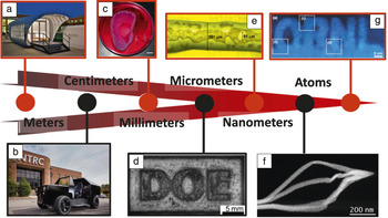
Mainstream approaches to 3D manufacturing include actuator systems that spatially constrain the solidifying precursor (e.g., molten plastic). Alternatively, high-energy beams can be used to induce melting and aggregation in powder beds, or polymerization in liquid monomers. The full scale of 3D fabrication is immense and spans meter-size dies for airplane parts to tens of microns-level details ( Figure 1 ). Reference Jones2–Reference Jesse, He, Lupini, Leonard, Oxley, Ovchinnikov, Unocic, Tselev, Fuentes-Cabrera, Sumpter, Pennycook, Kalinin and Borisevich8 On a smaller length scale, the electron-beam community has long been developing techniques based on direct electron-beam deposition, where the electron beam at the gas–solid interface results in the formation of decomposition products. Subsequent motion of the e-beam along a predefined path allows for the creation of intricate 3D structures, with feature sizes as small as tens of nanometers. While issues remain with the phase purity and crystallinity of these materials, the continuous progress in this direction holds promise for future advances.
Three-dimensional (3D) printing at different scales. (a) 38 × 12 × 13 feet3 3D printed house made for Oak Ridge National Laboratory’s (ORNL) Additive Manufacturing Integrated Energy demonstration project. Photo by C. Jones. Reference Jones2 (b) Three-dimensional printed natural-gas-powered hybrid electric vehicle for ORNL’s Additive Manufacturing Integrated Energy demonstration project. Photo by C. Jones. Reference Jones3 (c) Image of a 3D printed bionic ear. Scale bar = 1 cm. Reference Mannoor, Jiang, James, Kong, Malatesta, Soboyejo, Verma, Gracias and McAlpine4 (d) Energy-selective neutron radiograph of a 5-mm Inconel 718 sample. D, O, E are outlined using electron-beam additive manufacturing for control of crystallographic grain orientation. Reprinted with permission from Reference Reference Dehoff, Kirka, Sames, Bilheux, Tremsin, Lowe and Babu5. © 2015 Taylor & Francis Ltd. (e) Printed silver nanoparticle ink on polymeric substrate after sintering. Reprinted with permission from Reference Reference Zhou, List, Duty and Babu6. © 2015 Springer. (f) Plasmonic response of focused electron-beam-induced-deposition (FEBID)-based 3D Au nanostructures. High-angle annular dark-field (HAADF) survey image. Adapted with permission from Reference Reference Winkler, Schmidt, Haselmann, Fowlkes, Lewis, Kothleitner, Rack and Plank7. © 2017 American Chemical Society. (g) Example of crystalline oxide sculpting using an arbitrary graphical pattern (in this case, text “ORNL”): Fourier-filtered HAADF. Reference Jesse, He, Lupini, Leonard, Oxley, Ovchinnikov, Unocic, Tselev, Fuentes-Cabrera, Sumpter, Pennycook, Kalinin and Borisevich8

A natural question then arises: What is the limit of direct fabrication by an electron beam? The answer is inseparable from the analysis of the possible transformations that electron beams can induce in solids. One such interaction explored in the 1980s and 1990s is e-beam-induced mesoscopic crystallization and amorphization. Reference Yang, Wang, Yan and Zhang9–Reference Wang, Itoh, Matsunami and Zhao11 The remarkable progress in scanning transmission electron microscopy (STEM) now routinely enables atomic resolution. Correspondingly, a combination of atomically resolved STEM and e-beam-induced materials transformations can be used as a basis for 3D fabrication on the atomic level.
This article reviews the basic models for beam–solid interactions, illustrates the application of atomically resolved high-resolution STEM for atomic fabrication particularly in the quantum materials and devices domain, and discusses future applications.
E-beam effects in solids
Theoretical descriptions of electron microscopy and associated beam–matter interactions date back to the mid-20th century. This classical theory follows the mold of theories of scattering of high-energy particles, exploring dissimilar classes of scattering events and the associated cross sections. While the applications of this formalism to describing different types of experimental data continue to develop, and more precise ways of calculating cross sections are being proposed, the underlying framework remains unchanged from the classical picture.
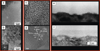
In (S)TEM, beam electrons can lose energy to the specimen through both elastic and inelastic scattering. Elastic scattering conserves kinetic energy and momentum between a beam electron and an atom. Inelastic scattering conserves total energy and momentum, while a part of the kinetic energy is converted into atom-electronic excitations. Besides being dissipated into heat, the energy gained by the specimen can also cause phase changes, such as amorphization and crystallization ( Figure 2 ). Reference Li, Zhang and Xu12–Reference Lulli and Merli14 Popular mechanisms to interpret these beam effects include knock-on interactions, radiolytic processes, damage by induced electric field (DIEF), and thermal effects. Reference Jiang15
High-resolution electron microscope (HREM) examples of crystallization of amorphous regions under electron-beam irradiation. (a–b) Amorphous GaAs and crystallization after 80 min of irradiation by electron beam (93 pA/cm Reference Jones2 ). Inset shows the corresponding selected-area electron diffraction pattern. Reprinted with permission from Reference Reference Li, Zhang and Xu12. © 2004 Elsevier. (c–d) Amorphous Ge0.7Si0.3 film and crystallization induced by 17 min of electron-beam irradiation with current density of 450 pA/cm2. Reprinted with permission from Reference Reference Xu and Ngan13. © 2004 Taylor & Francis Ltd. (e–f) HREM image of a thin region of a self-implanted Si sample in (110) projection, before and after irradiation with 300 keV electrons for 28 min at room temperature. The dotted line in (f) indicates the position of the original amorphous–crystalline interface. Reprinted with permission from Reference Reference Lulli and Merli14. © 1993 American Physical Society.

Knock-on interaction results in energy and momentum transfer from an energetic electron to an atom following collision. To displace an atom, a minimum kinetic energy of beam electrons is required. The threshold beam energy is proportionally dependent on the atomic mass and its threshold displacement energy, E d. Another important parameter is knock-on cross section (σ), which is the probability for knock-on occurrence per incident electron. Sophisticated formulae for σ can be derived from both classical and quantum mechanical theories, Reference Reimer16 but a simplified equation, Reference Hobbs, Chapman and Craven17 σ = 70Z/E d (where Z is the atomic number), provides a convenient approximation. It shows that the possibility of knock-on events is inversely dependent on E d. Considering that a (S)TEM specimen is usually very thin, the surface-to-volume ratio is large. In addition, the threshold surface sputtering energy is only a fraction of E d for the bulk displacement. Reference Egerton, McLeod, Wang and Malac18 Therefore, knock-on interaction is more likely to cause preferential surface sputtering than the formation of any type of bulk defects or phase changes. This may change as the surface-to-volume ratio decreases for thicker samples, provided both sample parameters (mean free path) and the optical setup (small focus depth and ability to focus inside the sample) allow for the confinement of the affected region away from the sample surface.
Radiolytic processes occur due to the decay of electronic excitations, which can break chemical bonds, initiate atom displacements, and produce point defects driven by either thermal vibrations or local Coulomb repulsive forces. Reference Kabler and Williams19,Reference Hobbs and Pascucci20 For radiolysis to occur, the excitations should remain localized long enough for an atom to respond mechanically. Reference Hobbs21 In the past, radiolysis has been considered as the main mechanism for beam effects in insulating materials. However, this conjecture is now being questioned as the observed phenomena rarely result in individual point defects. They are usually the consequence of massive collective atomic displacements, resulting in phase decomposition or phase transformation. Even if all the displaced atoms were initially radicals produced by the radiolytic processes or affected by the radicals, the question remains as to how the same species associate or dissociate collectively and rapidly. Reference Jiang15
The origin of the electron-beam-induced electric field in (S)TEM is different from the electron deposition in a bulk scanning electron microscope (SEM) specimen, since all the beam electrons in STEM pass through the specimen in transmission geometry. The charging process in a (S)TEM specimen is initiated by the excitations of atomic electrons, and if the holes left by the emissions cannot be neutralized in a certain period of time (e.g., in an insulator or a wide-gap semiconductor), the accumulation of positive charges results. Reference Humphreys22–Reference Jiang24 To displace an atom (cause damage), the field produced by the accumulated positive charges must be strong enough to overcome the binding energy of this atom (or its activation energy for migration).
There are two thresholds below which DIEF does not occur. Reference Jiang24–Reference Jiang26 One is the threshold electron-beam current density (or dose rate) and the other is the threshold exposure time (or incubation period). Since it is driven by the electric field, DIEF is a result of the simultaneous displacements of all the affected ions, with cations moving toward one direction and anions to the opposite. One of the important parameters that govern the DIEF mechanism is the electronic conductivity of the specimen. During the damage (i.e., massive atomic migration), the conductivity of the illuminated sample could either decrease or increase. A change in conductivity can, in turn, affect the charge accumulation, and thus the induced electric field. Reduced conductivity can aggravate, while increased conductivity can thwart, the damage process. Therefore, two general results can be expected from the DIEF mechanism—one is phase separation, which results from a decrease in conductivity, and the other is phase transformation, which is a result of the increase in conductivity. Reference Jiang24 In experiments, phase separation also includes precipitation of nanoparticles and formation of gas bubbles by electron irradiation.
The temperature rise in a TEM specimen is due to energy transfer from the beam to the specimen via electron–phonon scattering Reference Reimer16,Reference Brown, Sundararaman, Narang, Goddard and Atwater27 and it is determined by the total energy absorbed by the specimen from the electron beam as well as the quality of the thermal contact between the specimen and the specimen support. However, the latter may vary from case to case, and it is almost impossible to judge the validity of each individual experiment based on the limited information in the literature. Therefore, heating effects by the electron beam remain a matter of controversy and active debate in the experimental and theory community alike. Nevertheless, many experiments have shown that phase changes induced by electron irradiation are different from their thermal annealing counterparts. Reference Su, Jiang, Spence, He and Petuskey28–Reference Jiang and Spence30 In other words, while a rise of sample temperature during irradiation will certainly facilitate atomic diffusion and rearrangement of the lattice, Reference Su31 beam damage should not just be modeled as equivalent to a temperature increase in the bulk material.
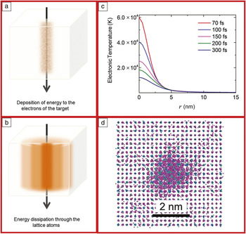
Of special interest for electron-beam-induced manipulation are the mechanisms of elastic energy loss. Here, energy deposited in the electronic system results in the excitation of the target electrons, which interact with lower temperature electrons ( Figure 3a). Subsequently, the electrons interact with the lattice atoms via electron–phonon coupling, transferring energy to them that later dissipates through the lattice atoms (Figure 3b).
(a) Energy is transferred to the electrons of the target material. (b) Following electron–phonon interaction and energy transfer from the electrons to the atoms, the energy dissipates among the atoms. (c) Electronic temperature profiles of predamaged SrTiO3 at different times after an irradiation event with 21 MeV Ni ions. (d) Formation of an amorphous ion track in predamaged SrTiO3 due to 21 MeV Ni ions. Reference Zarkadoula, Pakarinen, Xue, Zhang and Weber36

The energy exchange between the electronic and the atomic subsystems can be described by a two-temperature (2T) model. Reference Kaganov, Lifshitz and Tanatarov32,Reference Meftah, Costantini, Djebara, Khalfaoui, Stoquert, Studer and Toulemonde33 In the 2T model, the energy dynamics are described via a set of heat diffusion equations, one describing the evolution of the electronic temperature T e (Equation 1) and one describing the evolution of the atomic temperature T a (Equation 2):
 $$C_{\rm{e}} \left( {T_{\rm{e}} } \right){{\partial T_{\rm{e}} } \over {\partial t}} = {1 \over r}{\partial \over {\partial r}}\left[ {r\,K_{\rm{e}} \left( {T_{\rm{e}} } \right){{\partial T_{\rm{e}} } \over {\partial r}}} \right] - g\left( {T_{\rm{e}} - T_{\rm{a}} } \right) + S\left( {r,t} \right);$$
 $$C_{\rm{a}} \left( {T_{\rm{a}} } \right){{\partial T_{\rm{a}} } \over {\partial t}} = {1 \over r}{\partial \over {\partial r}}\left[ {rK_{\rm{a}} \left( {T_{\rm{a}} } \right){{\partial T_{\rm{a}} } \over {\partial r}}} \right] + g\left( {T_{\rm{e}} - T_{\rm{a}} } \right).$$
Here, C e and C a are the heat capacities of the electronic and the atomic systems, K e and K a are the electronic and lattice thermal conductivity, and g is an electron–phonon coupling parameter. The term S (r, t) describes the spatial and temporal energy deposition from the incident particle to the electrons.
The strength of the interaction is relevant to the electron–phonon coupling matrix (usually approximated by a coupling parameter Reference Brown, Sundararaman, Narang, Goddard and Atwater27,Reference Brown, Sundararaman, Narang, Schwartzberg, Goddard and Atwater34 ), and the energy exchange depends on the temperature difference between the two subsystems. With parameters such as the specific heat, the thermal conductivity of the electronic and the atomic subsystems, and the electron–phonon coupling strength known, the energy deposition to the atomic system can be calculated, and used in simulations to confirm or predict the experiment. A vast majority of studies treat these material parameters as phenomenological temperature-independent constants. However, a key challenge in the quantitative application of the 2T model is the determination of these temperature-dependent material parameters. Conventional 2T analyses track the time dependence (optionally the spatial variation) of separate electron and lattice temperatures, which implicitly neglects nonequilibrium effects of the electrons. Nonequilibrium effects can be neglected in certain cases (including those discussed here), however, these could be critical in the context of atom-by-atom fabrication.
For example, Figure 3c illustrates the electronic temperature profiles obtained with the 2T model within the inelastic thermal spike (iTS) model Reference Toulemonde, Assmann, Dufour, Meftah, Studer and Trautmann35 for ion irradiation. These curves describe the spatial and temporal evolution of the electronic temperature in irradiated SrTiO3 containing a small level of preexisting defects with 21 MeV Ni ions. Figure 3d illustrates the resulting damage for these irradiation conditions. While the energy loss from 21 MeV Ni ions does not produce damage in pristine crystalline SrTiO3, preexisting defects act synergistically with the electronic energy loss, resulting in the creation of an amorphous ion track. Reference Zarkadoula, Pakarinen, Xue, Zhang and Weber36,Reference Weber, Zarkadoula, Pakarinen, Sachan, Chisholm, Liu, Xue, Jin and Zhang37 This indicates that energy dissipation through the material can be affected by the microstructure, such as the presence of preexisting disorder. The preexisting defects can alter the thermal conductivity and affect the electron–phonon coupling strength by acting as scattering centers. Both the preexisting disorder and the electron–phonon coupling strength can affect the way the energy dissipates in the target material. Additionally, it would be easier for the preexisting defects to percolate during irradiation and potentially contribute to any beam-induced structure alterations. Accordingly, the energy deposition would differ between a pristine crystalline system and its amorphous state.
Overall, the electronic and the nuclear energy loss, separately or combined, can have different effects on the material response to radiation. Energy deposition and dissipation in matter are complex processes that depend both on the particle type and energy and on the target’s characteristics. Good theoretical understanding of these microscopic processes and linking the temperature and charge dynamics under the beam irradiation would enable selective alterations of the structure and creation of unusual microstructures and functionalities in the system.
Atomic fabrication via e-beams
Aberration correction in STEM has enabled sub-angstrom electron probes, opening new possibilities in beam-induced material modification. Reports point to the ability of the aberration-corrected probes to create highly localized holes in graphene Reference Girit, Meyer, Erni, Rossell, Kisielowski, Yang, Park, Crommie, Cohen, Louie and Zettl38–Reference Song, Schneider, Xu, Pandraud, Dekker and Zandbergen40 and induce the formation of crystalline nanowires between holes in MoS2. Reference Lin, Cretu, Zhou, Suenaga, Prasai, Bolotin, Cuong, Otani, Okada, Lupini, Idrobo, Caudel, Burger, Ghimire, Yan, Mandrus, Pennycook and Pantelides41 Additional patterning approaches should also be possible given the nanometer-scale focus depth of the aberration-corrected probe Reference Borisevich, Lupini and Pennycook42 that could help confine the impact volume inside the bulk materials and therefore enable beam-induced transformation pathways beyond drilling holes.
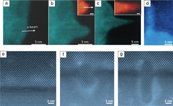
Experimental evidence of this reasoning was recently provided in reports on beam-induced epitaxial crystallization in SrTiO3. Reference Jesse, He, Lupini, Leonard, Oxley, Ovchinnikov, Unocic, Tselev, Fuentes-Cabrera, Sumpter, Pennycook, Kalinin and Borisevich8,Reference Zhang, Lian, Wang, Jiang, Ewing and Weber43 In this work, an amorphous SrTiO3 layer on top of a crystalline SrTiO3 substrate could be locally crystallized while maintaining full epitaxial registry. The process proceeded much faster at an accelerating voltage of 200 kV, even though the effect was still present at 100 kV and even 60 kV. To enable epitaxial growth, the beam path had to start at the substrate, which served as a seed. For a linear beam path and constant electron dose, the crystallization appeared to decelerate as the probe traveled further away from the substrate, eventually stopping and resulting in features of a characteristic conical shape ( Figure 4a–c). The observed behavior led the authors to deduce that the process is driven by knock-on interactions (knock-on cross section increases with accelerating voltage). The conical shape was attributed to diffusion effects, as the forming features also appeared to attract additional material toward themselves during the growth. The authors were able to demonstrate that the composition of the growing features did not measurably differ from that of the substrate. Reference Jesse, He, Lupini, Leonard, Oxley, Ovchinnikov, Unocic, Tselev, Fuentes-Cabrera, Sumpter, Pennycook, Kalinin and Borisevich8,Reference Zhang, Lian, Wang, Jiang, Ewing and Weber43
Epitaxial scanning transmission electronic microscope (STEM) patterning at amorphous–crystalline interfaces. (a–d) Patterning in SrTiO3. (a–c) Characteristic conical shape created with a linear beam path and constant electron dose. Insets show close-ups of the tip of the growing feature (scale bars = 1 nm). (d) “L” pattern using the optimized probe parameters and advanced scan control. Reference Jesse, He, Lupini, Leonard, Oxley, Ovchinnikov, Unocic, Tselev, Fuentes-Cabrera, Sumpter, Pennycook, Kalinin and Borisevich8 (e) Pristine Si/amorphous Si interface; (f–g) crystalline features generated with beam-induced growth at 200 kV.

It was further possible to optimize the growth conditions to alleviate the conical effect and enable full control of the growing shapes. To achieve that, an advanced scan control system was designed and implemented to bypass the standard rectangular scan mode, which is the only one available on most high-resolution microscopes. Using this setup, the authors were able to generate fine crystalline features, such as the letter “L” shown in Figure 4d. Reference Jesse, He, Lupini, Leonard, Oxley, Ovchinnikov, Unocic, Tselev, Fuentes-Cabrera, Sumpter, Pennycook, Kalinin and Borisevich8 This feature is about 7-nm wide and 40-nm tall. While these sizes are on par with the smallest achievable with electron lithography, the epitaxial character of the growth and the ability to induce the effect inside the volume of the amorphous material sets this method apart from other patterning approaches.
While the proposed mechanisms are quite general, experimental confirmation is needed on whether this growth approach is feasible in materials other than oxides, or indeed other than SrTiO3. Therefore, a similar experiment was attempted using a Si/amorphous Si interface. Figure 4e shows the appearance of the pristine interface, with the crystalline Si in (110) orientation. Figure 4f–g show different stages of beam-induced growth of crystalline features at this interface. Overall rate of feature growth was slower than in the case of SrTiO3. Also the feature in Figure 4g appears to have stacking faults. It is not clear what is the driving force for these deviations from the epitaxial growth character in the absence of strain; possibilities include anisotropic excitation propagation in the Si lattice and influence of oxygen trapped at the crystalline–amorphous interface. Modeling work to evaluate and differentiate these explanations is currently underway.
Perspectives
Direct atomic-beam patterning of solids opens new pathways for direct fabrication of atomic-scale structures, with concurrent fabrication and observation steps. One application of atomic-beam fabrication is in the realm of quantum defects to create bright and photostable quantum emitters based on atomic defects in 2D materials, including room-temperature single-photon emitters that are spectrally tunable Reference Tran, Bray, Ford, Toth and Aharonovich44 as well as spectrally narrow. But the search for atomically designed quantum emitters has just begun. Two-dimensional and 3D materials and defects in these materials offer a new pathway to quantum defects. Engineering defects in materials allow atomic-scale sculpting of localized quantum systems with desirable properties. While the crystallographic origin of quantum emitters is extremely challenging to determine in bulk 3D materials, recent advances allow structural determination using atomic-scale STEM imaging. Notably, designed materials allow for control of electron–phonon coupling (coupling to the phonon bath) and spin bath interactions. Theoretical predictions and simulations of such interactions in materials are the subject of active research. The ability to design electronic defects in materials using quantum chemistry simulations, together with the capacity to experimentally produce these “trapped molecules,” makes this material platform promising for atom-up control, design, and scaling of quantum information processing and sensing systems. Reaching this goal will require a combination of advanced theory and simulation tools, atomic-scale fabrication techniques, and scaling to mid- and large-scale quantum systems.

Nan Jiang is a scientist in the Department of Physics at Arizona State University. He received his PhD degree in materials science from the University of Birmingham, UK, and his BSc degree in physics from Jilin University, China. Prior to his current position, he was a postdoctoral researcher at Cornell University. His current interests include the fundamentals of beam effects in solid and liquid matter in (scanning) transmission electron microscopy, and electron energy-loss spectroscopy in beam-sensitive materials. Jiang can be reached by email at nan.jiang@asu.edu.

Eva Zarkadoula is a R&D associate in the Materials Science and Technology Division at Oak Ridge National Laboratory (ORNL). She received her PhD degree in physics from Queen Mary University of London, UK, in 2013, and her BSc degree in physics from the University of Athens, Greece. Prior to her current position, she was a postdoctoral researcher in atomistic modeling at ORNL. Her current research focuses on the interaction of radiation with matter and the fundamental effects of electronic excitations in the energy dissipation, damage creation, and microstructural alterations, which she investigates with the use of modeling techniques. Zarkadoula can be reached by email at zarkadoulae@ornl.gov.

Prineha Narang is an assistant professor in the John A. Paulson School of Engineering and Applied Sciences at Harvard University. She was a Ziff Environmental Fellow at the Harvard University Center for the Environment to explore the new field of excited-state quantum materials and devices. She received her ScB degree in materials science from Drexel University, and her MS and PhD degrees in applied physics as a National Science Foundation Graduate Fellow and Resnick Sustainability Institute Fellow from the California Institute of Technology. Her current research interests include excited-state and ultrafast optoelectronic materials, atomic-scale engineering, imaging, and sensing technologies. Narang can be reached by email at pnarang@fas.harvard.edu.

Artem Maksov is a doctoral candidate at the Bredesen Center for Interdisciplinary Research and Graduate Education at The University of Tennessee, Knoxville, and a research assistant at the Center for Nanophase Materials Sciences, Oak Ridge National Laboratory. He received his BSc degree in chemistry from the University of Massachusetts Amherst. His research focuses on utilizing machine learning techniques informed by modeling and physical constraints to extract information from electron and scanning probe microscopy experiments. Maksov can be reached by email at amaksov@vols.utk.edu.

Ivan Kravchenko is an R&D staff member at the Center for Nanophase Materials Sciences at Oak Ridge National Laboratory (ORNL). He obtained his MS degree in materials science from Kyiv State University, Ukraine, and his PhD degree in solid-state physics from the Institute of Metal Physics of the National Academy of Sciences of Ukraine. Prior to joining ORNL, he was a postdoctoral associate at the University of Wisconsin–Madison and R&D staff member at the Nanoscience Institute for Medical and Engineering Technology at the University of Florida. His current research interests include nanofabrication techniques and studies of optical properties of nanometer-scale structured metallic, semiconductor, and dielectric metamaterials, and wide-band semiconductors and devices. Kravchenko can be reached by email at kravchenkoii@ornl.gov.

Albina Borisevich has been a senior researcher in the Materials Science and Engineering Division of Oak Ridge National Laboratory (ORNL) since 2014. She obtained her MSc and PhD degrees from the University of Pennsylvania, and held a postdoctoral position at ORNL. Her research focuses on developing new electron microscopy-based methods for quantitative structural analysis and directed patterning of defects and interfaces in complex oxides. Borisevich can be reached by email at albinab@ornl.gov.

Stephen Jesse has been a senior researcher at the Center for Nanophase Materials Sciences at Oak Ridge National Laboratory (ORNL), since 2016, and leader of the Directed Nanoscale Transformations Theme. He obtained his PhD degree from The University of Tennessee, Knoxville, and held a postdoctoral position at ORNL. His research focuses on developing new imaging and manipulation for scanning probe and electron microscopies, as well as developing advanced analysis methods of spectral-imaging data. Jesse can be reached by email at sjz@ornl.gov.

Sergei V. Kalinin is the director of the Oak Ridge National Laboratory (ORNL) Institute for Functional Imaging of Materials, and a distinguished research staff member at the Center for Nanophase Materials Sciences (CNMS) at ORNL since 2002. He also holds a joint associate professor position in the Department of Materials Science and Engineering at The University of Tennessee, Knoxville. He received his PhD degree from the University of Pennsylvania in 2002, followed by a Wigner Fellowship at ORNL (2002–2004). His research interests include application of big data, deep data, and smart data approaches in atomically resolved and mesoscopic imaging to guide the development of advanced materials for energy and information technologies, as well as electromechanical, electrical, and transport phenomena and matter patterning on the nanoscale via scanning probe and electron microscopy. He is a recipient of several awards, including the RMS Medal for Scanning Probe Microscopy (2015) and the Presidential Early Career Award for Scientists and Engineers (2009); three R&D 100 Awards (2008, 2010, and 2016); and a number of other distinctions. He has published more than 500 papers, edited three books, and holds more than 16 patents. Kalinin can be reached by email at sergei2@ornl.gov.